EP0696817B1 - Einrichtung zur Kopplung von Be- und Entladegeräten mit Halbleiterbearbeitungsmaschinen - Google Patents
Einrichtung zur Kopplung von Be- und Entladegeräten mit Halbleiterbearbeitungsmaschinen Download PDFInfo
- Publication number
- EP0696817B1 EP0696817B1 EP94118699A EP94118699A EP0696817B1 EP 0696817 B1 EP0696817 B1 EP 0696817B1 EP 94118699 A EP94118699 A EP 94118699A EP 94118699 A EP94118699 A EP 94118699A EP 0696817 B1 EP0696817 B1 EP 0696817B1
- Authority
- EP
- European Patent Office
- Prior art keywords
- loading
- semiconductor processing
- processing machine
- housing
- magazine
- Prior art date
- Legal status (The legal status is an assumption and is not a legal conclusion. Google has not performed a legal analysis and makes no representation as to the accuracy of the status listed.)
- Expired - Lifetime
Links
Images





Classifications
-
- H—ELECTRICITY
- H10—SEMICONDUCTOR DEVICES; ELECTRIC SOLID-STATE DEVICES NOT OTHERWISE PROVIDED FOR
- H10P—GENERIC PROCESSES OR APPARATUS FOR THE MANUFACTURE OR TREATMENT OF DEVICES COVERED BY CLASS H10
- H10P72/00—Handling or holding of wafers, substrates or devices during manufacture or treatment thereof
- H10P72/50—Handling or holding of wafers, substrates or devices during manufacture or treatment thereof for positioning, orientation or alignment
-
- H—ELECTRICITY
- H10—SEMICONDUCTOR DEVICES; ELECTRIC SOLID-STATE DEVICES NOT OTHERWISE PROVIDED FOR
- H10P—GENERIC PROCESSES OR APPARATUS FOR THE MANUFACTURE OR TREATMENT OF DEVICES COVERED BY CLASS H10
- H10P72/00—Handling or holding of wafers, substrates or devices during manufacture or treatment thereof
- H10P72/30—Handling or holding of wafers, substrates or devices during manufacture or treatment thereof for conveying, e.g. between different workstations
- H10P72/34—Handling or holding of wafers, substrates or devices during manufacture or treatment thereof for conveying, e.g. between different workstations the wafers being stored in a carrier, involving loading and unloading
- H10P72/3408—Docking arrangements
-
- B—PERFORMING OPERATIONS; TRANSPORTING
- B65—CONVEYING; PACKING; STORING; HANDLING THIN OR FILAMENTARY MATERIAL
- B65G—TRANSPORT OR STORAGE DEVICES, e.g. CONVEYORS FOR LOADING OR TIPPING, SHOP CONVEYOR SYSTEMS OR PNEUMATIC TUBE CONVEYORS
- B65G49/00—Conveying systems characterised by their application for specified purposes not otherwise provided for
- B65G49/05—Conveying systems characterised by their application for specified purposes not otherwise provided for for fragile or damageable materials or articles
- B65G49/07—Conveying systems characterised by their application for specified purposes not otherwise provided for for fragile or damageable materials or articles for semiconductor wafers Not used, see H10P72/00
-
- Y—GENERAL TAGGING OF NEW TECHNOLOGICAL DEVELOPMENTS; GENERAL TAGGING OF CROSS-SECTIONAL TECHNOLOGIES SPANNING OVER SEVERAL SECTIONS OF THE IPC; TECHNICAL SUBJECTS COVERED BY FORMER USPC CROSS-REFERENCE ART COLLECTIONS [XRACs] AND DIGESTS
- Y10—TECHNICAL SUBJECTS COVERED BY FORMER USPC
- Y10S—TECHNICAL SUBJECTS COVERED BY FORMER USPC CROSS-REFERENCE ART COLLECTIONS [XRACs] AND DIGESTS
- Y10S414/00—Material or article handling
- Y10S414/135—Associated with semiconductor wafer handling
- Y10S414/14—Wafer cassette transporting
Definitions
- the invention relates to a device for coupling loading and unloading devices with semiconductor processing machine with which a retrofit of such Machines with SMIF technology taking ergonomic into account Requirements.
- SMIF boxes standard mechanical interface boxes
- the magazine in the compartments of which the semiconductor wafers are located, is fixed in a suitable manner on the bottom of the SMIF boxes, which have a relatively small closed volume. To load the processing machines, the magazines from the transport containers are z. B.
- FR-A-2 696 429 is a device according to the preamble of the claim 1 of the present application.
- a device for coupling discloses a loading and unloading device with a semiconductor processing machine.
- the object of the invention is therefore to devices which are used for SMIF technology are required to couple with semiconductor processing machines in the a subsequent integration of the SMIF technology is excluded, whereby the after the coupling required have a high flexibility and one increasing size of the semiconductor wafers.
- the task is accomplished by a device for coupling loading and unloading devices solved with semiconductor processing machines according to claim 1.
- the receiving element can either be an adjustable one connected to a lift Plate can be or the adjustable plate is horizontal from one attached to the lift movable element worn.
- the advantage of a horizontally displaceable receiving element is that with a single loading and unloading device all processing stations of a semiconductor processing machine can be supplied. There will be no stand for additional loading equipment needed.
- the housing with which a mini-clean room is created, which ensures a horizontal low-turbulence air flow (first air) through the magazines in every phase of the loading of the semiconductor processing machine, taking into account the different loading methods of a fixed outer part and an extendable inner part, which encloses the receiving element together with the loading and unloading device.
- the inner part can be telescopically extended and retracted together with the receiving element and the loading and unloading device.
- At least one closure element is provided on the extendable inner part of the housing for closing loading openings in the semiconductor processing machine.
- both parts of the housing also have holes when the inner part is immersed in the outer part of the housing facing away from the semiconductor processing machine.
- the inner part may have holes in its bottom for the benefit of gas flow.
- the coupling element can advantageously be a semiconductor processing machine adjustable base plate with bevelled front edge, in which there is a positive, Coordinate orientation of spherical cap support screws in shaped elements drop.
- a permanent magnet that can be switched over in its force can be attached to the fixed one for attachment Part of the enclosure.
- the mobile device according to the invention can be used to set up a loading and unloading device in a coordinate-compatible manner with respect to a semiconductor processing machine.
- the device is to be attached to the loading and unloading device in a stable manner and largely decoupled in terms of vibrations from the semiconductor processing machine.
- the device can be removed from the semiconductor processing machine in a very short time and in an uncomplicated manner and can be reproducibly moved back on.
- this solution does not require any adjustment points or locking devices on the semiconductor processing machine A hindrance due to elements protruding beyond the projected area of the loading robot is excluded, which ensures that two devices according to the invention are very close to one another and to the semiconductor processing machine.
- magazines for semiconductor wafers that deviate from the standard with regard to connection dimensions, dimensions, wafer capacity or material have to be used more and more frequently. If a semiconductor factory is continuously equipped with the SMIF standard, this can result in restrictions or disruptions in the normal production process.
- a plate part which can be lowered in the interior of the loading and unloading device, in addition to a transport container for a magazine as the loading object, can also accommodate the magazine itself as the loading object.
- an adapter is connected to the plate part, on which the magazine can be placed and which takes over the function of the bottom of the SMIF box.
- the adapter has on a base plate at least one guide with mutually parallel guide edges, between which the magazine is placed with a web that connects opposite magazine walls of the magazine.
- a pair of lowerable elements guided through the base plate transmit simultaneous actuation through the magazine walls in the parked state of the magazine via connecting elements to sensors in the plate part.
- magazines can be loaded and unloaded exclusively is designed for the SMIF technology to be transported because of the mechanical detection and transmission system with attached magazines the detector system usually located in the plate part (SMIF port) can be recognized.
- the lift for the receiving element can be driven by a stepper motor which is connected to a voltage-dependent motor brake. Furthermore, gas pressure springs can support the lift against the fixed part.
- the fixed part can carry a movable safety bar, in which objects lying on a contact break of an otherwise closed Generate circuit, whereby the stepper motor is switched off.
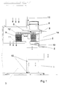
- a device 1 shown in Fig. 1 carries as a loading and unloading device 2, a transport device according to DE patent 43 26 309 C1. Instead of using this device, it is of course also possible to use devices with a different production process for loading and unloading a semiconductor processing machine 3.
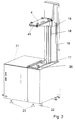
- An adjustable base plate 4 (FIG. 2) serves as the receiving element for the loading and unloading device 2 and can be moved between two superimposed levels 5, 6.
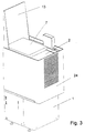
- Level 5 is at an ergonomically favorable height for loading the loading and unloading device 2, in which a transport container 8 in the form of an SMIF box can be placed as a loading object on a plate part 7 serving as an interface.
- level 6 which serves as the loading level, the SMIF pod is automatically opened and a magazine 9 is moved to a transfer height 11 by an elevator 10.
- a gripper 12 grips the magazine 9 and transports it into the semiconductor processing machine 3 by a linear movement.
- the magazine 9 is correspondingly removed from the semiconductor processing machine 3 with reverse sequence of steps.
- the device 1 can be coupled to the semiconductor processing machine 3 with releasable docking elements 15 or in a solution according to the Figures 10 to 13 take place.
- the adjustable base plate 4 which is on a mounting plate 41st is screwed on, for moving between the two superimposed levels 5, 6 on a vertically movable lift 16, which by a Stepper motor 17 is driven by an electric motor, attached.
- the rotary motion the stepper motor 17 is on a toothed belt, not shown, on a Threaded spindle 18 is transmitted and converted into a linear movement.
- a voltage-independent motor brake connected directly to the stepper motor 17 acts in the event of a power failure or emergency shutdown via an “emergency stop” switch (not shown here).
- the mass of the components moved in the vertical direction is compensated for by two gas pressure springs 19, one of which is visible.
- An executed safety bar 20 is another measure to increase security, especially to avoid of injuries to the operating personnel.
- One between the lift 16 and the Safety bar 20 object has a force on the safety bar 20 a break in the contact of an otherwise closed circuit and thus the immediate switching off of the stepping motor 17.
- the elevator 16 remains in the current position and is affected by the effect of the Compression springs 19 held.
- the device 1 is surrounded by a covering 21, which forms a vascular system, which also includes the control electronics, not shown here.
- the housing consists of a fixed outer part, the housing 24 and an inner part, the housing 25, which encloses the receiving element and the loading and unloading device 2 and can be telescopically extended for loading the semiconductor processing machine 3.
- the housing design ensures the necessary clean room conditions when loading or retrofitting the semiconductor processing machine with SMIF technology.
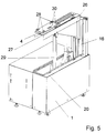
- a solution serves to expand the range of motion of the device 1 according to Figures 5 and 6, with which in addition to the superimposed levels 5, 6 also adjacent processing stations can be operated.
- the mounting plate 41 shown in FIG. 2 is used instead of the adjustable one Base plate 4 for receiving loading and unloading device 2, a unit 26 placed on it, capable of linear motion in the horizontal direction. Using appropriate mechanical fasteners (not shown), the adjustable base plate 4 is attached to this unit 26.
- the unit 26 consists of a U-shaped base body as a receptacle for a stepper motor 27 with a spindle drive (not shown) and a guide coupled therewith.
- the stepper motor 27 is monitored step by step via an encoder and monitored by electronic end position couplers in both end positions.
- a guided trailing cable 29 is used to connect the loading and unloading device 2 to be set up and held with fastening elements 28 to the electronic control. According to the mechanical design of the adjustable base plate 4 with a retrieval device 30, a quick change of the loading and unloading device 2 is possible.
- housings 31, 32 which in principle corresponds to the housing according to FIG. 4.
- the housing 32 is moved telescopically to the housing 31.
- a movable closure element 33 such as a door, a sliding flap or a roller blind-like closure, ensures that the inner clean room of the loading and unloading device 2 remains closed even during the lateral movement.
- FIG. 7 An example is shown in which the semiconductor processing machine 3 can also be loaded in a plane 34.
- the magazine 9 can be transported into the semiconductor processing machine 3 from the level 6 at a transfer height 11 and from the level 34 at a further transfer height 35. It is also possible with the loading and unloading device 2, from the levels 6 and 34, the magazine 9 in different positions 36, 37 or when using devices with a different functional sequence than in the transport device according to DE patent 43 26 309 C1 to park in other locations.
- the housing for loading and unloading devices 2 is shown in more detail with reference to FIGS. 8 to 11 described, the one facing away from the semiconductor processing machine 3 Own integrated filter-blower / fan unit 14, and which, as already described, mechanically firmly connected via an adjustable base plate 4 for Semiconductor processing machine 3 are adjustable in height and / or slidable.
- the housing shown in FIG. 8 consists of the fixed housing 24, in which the height-adjustable housing 25 of the loading and unloading device is integrated.
- the housing 25 is preferably formed by four antistatic and thus clean room-compatible plastic plates which are fixedly mounted on both side walls and the top and bottom of the loading and unloading device 2.
- Such a housing is suitable for one-day loading of semiconductor processing machines with a self-closing loading opening.
- Both housings 24, 25 are completely open on their front side facing the semiconductor processing machine 3.
- a distance of all wall parts adjacent to the semiconductor processing machine 3 is to be produced in such a way that mechanical contact during the height shift is excluded, but the clean room conditions remain undisturbed.
- Both housings have holes 38, 39 in their rear walls to ensure the suction or ventilation process even when the height-displaceable housing 25 is immersed in the fixed housing 24.
- the housing 25 is closed at the bottom by a base plate 40, into which holes 41 are incorporated, on the one hand to keep a vertical flow with throttling action / nozzle action along the front of the semiconductor processing machine 3 when the height-displaceable housing 25 is immersed / moved out into the fixed housing 24 and on the other hand to ensure an overpressure or a pressure drop in the mini-clean room formed in relation to the environment or the semiconductor processing machine 3.
- means, not shown, are provided for independent removal or removal. Switch on the filter blower / fan unit 14 when driving into or out of level 5, in which the loading and unloading device 2 is loaded with a SMIF box.
- FIG Shield running parallel to the front wall of the semiconductor processing machine 3 43 provided that when driving the loading and unloading device 2 in level 5 Feed opening 42 closes.
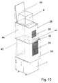
- two shields 45 are fixedly connected to the housing 25 in FIG. 10 in addition to the solution according to FIG. 9 parallel to the front wall of the semiconductor processing machine 3.
- the embodiment serves to load a parallel to the front wall of the semiconductor processing machine 3 in two superimposed levels, as shown in Fig. 7.
- the shields 45 are designed such that the part of the opening 44 of the semiconductor processing machine which is not loaded is always closed.
- shields which are firmly connected to the loading and unloading device 2, for closing the loading openings
- movable covers such as blinds suitable for clean rooms. Solutions can also be used which provide sliding doors of the semiconductor processing machine which are coupled to the movement of the loading and unloading devices.
- a flat base plate 48 which is adjusted to the semiconductor processing machine 3 and serves as a coupling element, is screwed to the floor in front of the semiconductor processing machine 3 for receiving the device 1 with the loading and unloading device 2.
- Suitable elements for the device 1 are located in the base plate 48 for reproducible, form-fitting retrieval of the adjusted position.
- the device 1 can be tilted together with the loading and unloading device 2 Condition on rollers 49 sack barrow to be moved away or up.
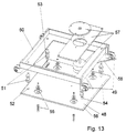
- spherical cap support screws 51 are adjustable in the vertical direction for docking in a base frame 50 in the area of the base of the device 1. These are set down in the elements cone 52, prism 53 and plane 54 located in the base plate 48 for positive, coordinate-oriented orientation.
- the bottom plate 48 is in turn screwed to the floor in accordance with the coordinates for the semiconductor processing machine 3 by means of screws 55.
- the front edge 56 of the base plate 48 is designed so that it serves for pre-orientation (estimate) for the opening of the rollers 49 and from this point the device is lowered after the sack-cart-like approach.
- the support screws 51 find the shaped elements 52, 53 and 54 of the base plate 48 itself.
- the static safety of the device 1 is preferably gimbaled adjustable permanent magnets 57 attached to the base frame 50. In the Working position of the device 1, the permanent magnet 57 to the highest holding force switched from the outside via an actuating lever 58. This is a non-positive Connection to the base plate 48 ensures a high level of stability.
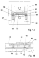
- the adapters shown in FIGS. 14 to 17 are suitable, depending on which one Semiconductor wafer dimensions are to be used, attached to the plate part 7 be, and to directly record a magazine 9 as a loading object.
- a contact rail 61 for 4 "magazines and a contact rail 62 for 6" magazines are located on a base plate 59, which corresponds to the dimensions of the plate part 7 in length, width and height, adjacent to a guide rail 60.
- the magazine wall 66 is assigned to a magazine of smaller size (4 ") and the magazine wall 67 to a magazine of larger dimensions (6").
- the magazine walls 66, 67 are connected to one another by connecting webs 69, 70, a so-called H-bar.
- the connecting webs 69, 70 are the elements of the magazines which are used for fixing on the base plate 59.
- an anvil 71 in the plate part 7 actuates sensors 72, which can also be designed as switches.
- the sensors 72 have the function of signaling the attached state.
- the arrangement of such sensors is e.g. B. in patent step DE 43 26 308 C1 with the further function of initiating a gas supply and discharge there.
- the spring 65 prevents the sensors 72 in the plate part 7 from being actuated in the unloaded state.
- the spring 65 is dimensioned such that a full or empty magazine actuates the sensors 72 safely. Simultaneous actuation of both bearing surfaces 68 is also necessary for the reliable detection of the deposited state.
- FIGS. 16 and 17 An embodiment of the adapter according to FIGS. 16 and 17 is provided for magazines with even larger dimensions (8 ").
- a guide rails 74 and a contact rail 75 are arranged on a base plate 73.
- a magazine which is connected with its web 77 connecting side walls 76 between the guide rail 74 and the contact rail 75, actuates, with the magazine walls 76, lowerable elements 78 which are simultaneously guided through the base plate 73.
- the magazine is also not completely shown, as in FIG. 14 .
- the bearing surfaces 78 are connected via webs 79 to a movable bar 80, so that actuating pins 81 which are resiliently fastened to the bar 80 can press the sensors provided in the plate part 7.
Landscapes
- Container, Conveyance, Adherence, Positioning, Of Wafer (AREA)
- Feeding Of Workpieces (AREA)
- Manufacturing Of Electrical Connectors (AREA)
Description
Auf dem Boden der SMIF-Boxen, die ein relativ Kleines abgeschlossenes Volumen aufweisen, ist das Magazin, in dessen Fächern sich die Halbleiterscheiben befinden, in geeigneter Weise fixiert.
Zur Beschickung der Bearbeitungsmaschinen werden die Magazine aus den Transportbehältern z. B. mit einer Be- und Entladeeinrichtung gemaß der DE-Patentschritt 43 26 309 C1 oder einer Einrichtung, mit anderen Funktionsablauf entladen und in der Bearbeitungsmaschine plaziert. Nach der Bearbeitung der Halbleiterscheiben erfolgt der Rücktransport der Magazine in die Transportbehälter. Da sich die räumliche Anordnung der Be- und Entladeeinrichtungen üblicherweise nach dem Bearbeitungszyklus in der Maschine richtet, wird deren Bestückung mit Magazinen oder Magazinen im Transportbehälter und damit die manuelle Beschickung der Bearbeitungsmaschinen bei zunehmender Größe der Halbleiterscheiben zum Problem.
Besondere Schwierigkeiten treten auf, wenn Maschinen der Halbleiterfertigung mit der SMIF-Technologie nachgerüstet werden sollen, da eine nachträgliche bauliche Integration in den seltensten Fällen möglich ist.
aus einem feststehenden äußeren Teil und einem ausfahrbaren inneren Teil, der das Aufnahmeelement zusammen mit der Be- und Entladeeinrichtung umschließt. Zur Verstellung des Aufnahmeelementes zwischen den übereinanderliegenden Ebenen ist der innere Teil zusammen mit dem Aufnahmeelement und der Be- und Entladeeinrichtung teleskopartig aus- und einfahrbar.
Beide Teile der Einhausung weisen zur Gewährleistung des Ansaug- oder Lüftungsprozesses auch beim Eintauchen des inneren in den äußeren Teil in ihrer zur Halbleiterbearbeitungsmaschine abgewandten Seite Bohrungen auf.
Außerdem kann der innere Teil zum Vorteil der Gasströmung in seinem Boden Löcher besitzen.
Zu Servicezwecken ist die Einrichtung in kürzester Zeit und in unkomplizierter Weise von der Halbleiterbearbeitungsmaschine entfernbar und kann reproduzierbar wieder angerückt werden.
Außerdem benötigt diese Lösung keine Justierpunkte bzw. Verriegelungseinrichtungen an der Halbleiterbearbeitungsmaschine
Eine Behinderung durch über die projezierte Fläche des Beschickungsroboter hinausragende Elemente ist ausgeschlossen, wodurch ein sehr enges Aneinanderrücken von zwei Einrichtungen gemäß der Erfindung nebeneinander und an die Halbleiterbearbeitungsmaschine gewährleistet ist.
Bei einer durchgehenden Ausrüstung einer Halbleiterfabrik mit dem SMIF-Standard können sich dadurch Einschränkungen oder Störungen im normal üblichen Produktionsablauf ergeben.
Dazu wird mit dem Plattenteil ein Adapter verbunden, auf dem das Magazin absetzbar ist und der die Funktion des Bodens der SMIF-Box übernimmt.
Der Adapter weist auf einer Grundplatte mindestens eine Führung mit parallel zueinander gerichteten Führungskanten auf, zwischen die das Magazin mit einem Steg, der gegenüberliegende Magazinwände des Magazins verbindet, abgestellt wird. Ein Paar absenkbarer, durch die Grundplatte hindurchgeführter Elemente überträgt eine gleichzeitige Betätigung durch die Magazinwände im abgestellten Zustand des Magazins über Verbindungselemente auf Sensoren in dem Plattenteil.
Desweiteren können Gasdruckfedern den Lift gegenüber dem feststehenden Teil abstützen.
- Fig. 1
- eine Einrichtung im angekoppelten Zustand an eine Halbleiterbearbeitungsmaschine
- Fig. 2
- die Einrichtung ohne Gehäuse
- Fig. 3
- die Einrichtung in einer Einstellung zur ergonomischen Bestückung einer Be- und Entladeeinrichtung
- Fig. 4
- die Einrichtung in einer Einstellung zur Beschickung einer Halbleiterbearbeitungsmaschine
- Fig. 5
- eine Einrichtung mit erweitertem seitlichen Beschickungsbereich
- Fig. 6
- die Einrichtung gemäß Fig. 5 in verkleidetem Zustand
- Fig. 7
- eine Einrichtung für zwei unterschiedliche Beschickungshöhen
- Fig. 8
- eine Einhausung für eine Beschickung von Halbleiterbearbeitungsmaschinen mit verschließbarer Beschickungsöffnung
- Fig. 9
- eine Einhausung für eine Beschickung von Halbleiterbearbeitungsmaschinen ohne Verschluß der Beschickungsöffnung
- Fig. 10
- eine Einhausung für eine zweietagige Beschickung von Halbleiterbearbeitungsmaschinen ohne Verschluß der Beschickungsöffnung
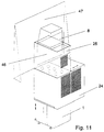
- Fig. 11
- eine Einhausung für eine einetagige Beschickung von zwei oder mehrere nebeneinanderliegenden Beschickungs- oder Entnahmestationen ohne Verschluß der Beschicküngsöffnung
- Fig. 12
- die Einrichtung auf einer Grundplatte justiert zur Halbleiterbearbeitungsmaschine abgestellt
- Fig. 13
- Mittel zur Ausrichtung und standsicheren Befestigung der Einrichtung gegenüber der Halbleiterbearbeitungsmaschine
- Fig. 14
- eine Aufsicht auf einen ersten Adapter für den separaten Einsatz eines Magazins ohne Transportbehälter in der Be- und Entladeeinrichtung
- Fig. 15
- der erste Adapter im Querschnitt
- Fig. 16
- eine Aufsicht auf einen zweiten Adapter
- Fig. 17
- der zweite Adapter im Querschnitt
Als Aufnahmeelement für die Be- und Entladeeinrichtung 2 dient eine justierbare Grundplatte 4 (Fig. 2), die zwischen zwei übereinanderliegenden Ebenen 5, 6 verfahrbar ist. Die Ebene 5 liegt in einer ergonomisch günstigen Höhe zur Beschickung der Be- und Entladeeinrichtung 2, in der auf einem als Schnittstelle dienenden Plattenteil 7 ein Transportbehälter 8 in Form einer SMIF-Box als Beschickungsgegenstand abstellbar ist. In der Ebene 6, die als Beschickungsebene dient, erfolgt eine automatische Öffnung des SMIF-Pods und ein Magazin 9 wird mit einem Fahrstuhl 10 in eine Übergabehöhe 11 gefahren. Ein Greifer 12 erfaßt das Magazin 9 und transportiert es durch eine Linearbewegung in die Halbleiterbearbeitungsmaschine 3.
Zusätzlich wird die Masse der in vertikaler Richtung bewegten Bauteile durch zwei Gasdruckfedern 19, von denen eine sichtbar ist, kompensiert.
Wie Fig. 4 zeigt, besteht die Einhausung aus einem feststehenden äußeren Teil, dem Gehäuse 24 und einem inneren Teil, dem Gehäuse 25, das das Aufnahmeelement und die Be- und Entladeeinrichtung 2 umschließt und für die Beschickung der Halbleiterbearbeitungsmaschine 3 teleskopartig ausfahrbar ist. Durch eine derartige Gehäusegestaltung werden die erforderlichen Reinstraumbedingungen bei der Beschickung bzw. bei der Nachrüstung der Halbleiterbearbeitungsmaschine mit der SMIF-Technologie gewährleistet.
Zur Verbindung der aufzusetzenden, mit Befestigungselementen 28 zu haltenden Be- und Entladeeinrichtung 2 mit der elektronischen Steuerung dient ein geführtes Schleppkabel 29.
Entsprechend der mechanischen Ausbildung der justierbaren Grundplatte 4 mit einer Wiederfindeinrichtung 30 ist ein schneller Wechsel der Be- und Entladeeinrichtung 2 möglich.
Durch ein bewegliches Verschlußelemente 33 wie z.B. einer Tür, einer Schiebeklappe oder ein rolloähnlicher Verschluß, wird gesichert, daß der innere Reinraum der Be- und Entladeeinrichtung 2 auch während der seitlichen Bewegung verschlossen bleibt.
Ein Beispiel wird in Fig. 7 gezeigt, in dem zusätzlich in einer Ebene 34 eine Beschickung der Halbleiterbearbeitungsmaschine 3 durchgeführt werden kann.
Das Magazin 9 ist von der Ebene 6 in einer Übergabehöhe 11 und von der Ebene 34 in einer weiteren Übergabehöhe 35 in die Halbleiterbearbeitungsmaschine 3 transportierbar.
Außerdem ist es mit der Be- und Entladeeinrichtung 2 möglich, von den Ebenen 6 und 34 aus das Magazin 9 in verschiedenen Positionen 36, 37 oder beim Einsatz von Einrichtungen mit anders gestaltetem Funktionsablauf als bei der Transportvorrichtung gemäß dem DE-Patent 43 26 309 C1 in anderen Lagen abzustellen.
Eine derartige Einhausung ist zur einetagigen Beschickung von Halbleiterbearbeitungsmaschinen mit selbstverschließbarer Beschickungsöffnung geeignet.
Beide Gehäuse weisen in ihren Rückwänden Bohrungen 38, 39 zur Gewährleistung des Ansaug- oder Lüftungsprozesses auch beim Eintauchen des höhenverschiebbaren Gehäuses 25 in das feststehende Gehäuse 24.
Das Gehäuse 25 ist nach unten durch eine Bodenplatte 40 abgeschlossen, in die Löcher 41 eingearbeitet sind um einerseits eine senkrechte Strömung mit Drosselwirkung/Düsenwirkung entlang der Vorderseite der Halbleiterbearbeitungsmaschine 3 beim Eintauchen/Herausfahren des höhenverschiebbaren Gehäuses 25 in das feststehende Gehäuse 24 gering zu halten und andererseits einen Überdruck oder ein Druckgefälle in dem gebildeten Mini-Reinstraum gegenüber der Umgebung bzw. der Halbleiterbearbeitungsmaschine 3 zu gewährleisten.
Außerdem sind nicht dargestellte Mittel vorgesehen für das selbständige Aus-bzw. Einschalten der Filter-Gebläse/Lüfter-Einheit 14 beim Fahren in bzw. aus der Ebene 5, in der die Be- und Entladeeinrichtung 2 mit einer SMIF-Box beschickt wird.
Die Schilde 45 sind so gestaltet, daß immer der nicht beschickte Teil der Öffnung 44 der Halbleiterbearbeitungsmaschine verschlossen wird.
Es sind auch Lösungen verwendbar, die mit der Bewegung der Be- und Entladegeräte gekoppelte Schiebetüren der Halbleiterbearbeitungsmaschine vorsehen.
In der Bodenplatte 48 befinden sich für ein reproduzierbares formschlüssiges Wiederfinden der justierten Lage für die Einrichtung 1 geeignete Elemente.
Über Schrauben 55 ist die Bodenplatte 48 wiederum koordinatengerecht zur Halbleiterbearbeitungsmaschine 3 mit dem Fußboden fest verschraubt.
Die Vorderkante 56 der Bodenplatte 48 ist so gestaltet, daß diese zur Vororientierung (Voranschlag) für die Auffahrt der Rollen 49 dient und von dieser Stelle aus das Absenken der Einrichtung nach der sackkarrengemäßen Anfahrt erfolgt.
Die Stützschrauben 51 finden die Formelemente 52, 53 und 54 der Bodenplatte 48 selbst.
Ein unterhalb der Grundplatte 59 angeordneter Winkel 63, der über ein einseitiges Gelenk 64 gelagert und durch eine Feder 65 abgestützt ist, wird von seitlichen Magarinwänden 66 oder 67 von abgesetzten Magazinen über ein durch die Grundplatte 59 hindurchgeführtes absenkbares Element 68 betätigt. Die Magazinwand 66 ist einem Magazin kleinerer Größe (4") und die Magazinwand 67 einem Magazin größerer Abmessungen (6") zugeordnet. Bei beiden Magazinen sind die Magazinwände 66, 67, dem SEMI-Standard entsprechend, durch Verbindungsstege 69, 70, einem sogenannten H-bar miteinander verbunden. Die Verbindungsstege 69, 70 sind die Elemente der Magazine, die zur Fixierung auf der Grundplatte 59 dienen.
Durch die Betätigung des Winkels 63 erfolgt in dem Plattenteil 7 über einen Amboß 71 eine Betätigung von Sensoren 72, die auch als Schalter ausgebildet sein können. Die Sensoren 72 haben neben anderen Aufgaben die Funktion, den aufgesetzten Zustand zu signalisieren. Die Anordnung derartiger Sensoren ist
z. B. in der Patentschritt DE 43 26 308 C1 mit der dortigen weiteren Funktion der Einleitung einer Gaszufuhr und -ableitung dargestellt.
Die Feder 65 verhindert, daß im unbelasteten Zustand die Sensoren 72 im Plattenteil 7 betätigt werden. Die Feder 65 ist so bemessen, daß ein volles oder leeres Magazin die Sensoren 72 sicher betätigt. Für die sichere Erkennung des abgesetzten Zustandes ist ebenfalls die gleichzeitige Betätigung beider Auflageflächen 68 erforderlich.
Auf einer Grundplatte 73 sind eine Führungsschienen 74 und eine Anlageschiene 75 angeordnet. Ein mit seinem, Seitenwände 76 verbindenden Steg 77 zwischen die Führungsschiene 74 und die Anlageschiene 75 abgestelltes Magazin betätigt mit den Magazinwänden 76 gleichzeitig durch die Grundplatte 73 hindurchgeführte, absenkbare Elemente 78. Der Übersicht halber ist das Magazin ebenso wie in Fig. 14 nicht vollständig dargestellt. Die Auflageflächen 78 sind über Stege 79 mit einer beweglichen Leiste 80 verbunden, so daß an der Leiste 80 federnd befestigte Betätigungsstifte 81 die in dem Plattenteil 7 vorgesehenen Sensoren drücken können.
Claims (13)
- Einrichtung zur Kopplung einer Be- und Entladeeinrichtung (2) mit einer Halbleiterbearbeitungsmaschine (3), mit einer fahrbaren Einhausung, innerhalb derer ein justierbares Aufnahmeelement (4) für die Be- und Entladeeinrichtung (2) vorgesehen ist, das zwischen mindestens zwei übereinanderliegenden Ebenen (5,6) verstellbar ist, von denen eine (5) der Bestückung der Be- und Entladeeinrichtung (2) und jede andere (6) zur Beschickung der Halbleiterbearbeitungsmaschine (3) durch die Be- und Entladeeinrichtung (2) dient, dadurch gekennzeichnet, daß die Einhausung Ausricht- und Halteelemente (49,50,51,57) zur Befestigung an einem zur Halbleiterbearbeitungsmaschine (3) ausgerichteten Ankoppelelement (48,52-56) aufweist und aus einem feststehenden äußeren Teil (24) sowie einem aus diesem teleskopartig ausfahrbaren und zwischen den übereinanderliegenden Ebenen (5,6) verfahrbaren inneren Teil (25) besteht, welches das Aufnahmeelement zusammen mit der Be- und Entladeeinrichtung (2) umschließt, wobei jeweils auf der von der Halbleiterbearbeitungsmaschine (3) abgewandten Rückwand die Be- und Entladeeinrichtung (2) mit einer ein Filter und ein Gebläse umfassenden Einheit (14) und das äußere (24) wie auch das innere (25) Teil der Einhausung jeweils in seiner von der Halbleiterbearbeitungsmaschine abgewandten Seite mit Bohrungen (38,39) versehen ist.
- Einrichtung nach Anspruch 1, dadurch gekennzeichnet, daß das Aufnahmeelement eine mit einem Lift (16) verbundene justierbare Platte (4) ist.
- Einrichtung nach Anspruch 1, dadurch gekennzeichnet, daß das Aufnahmeelement eine von einem horizontal beweglichen, auf einem Lift (16) befestigten Element (26) getragene justierbare Platte (4) ist.
- Einrichtung nach einem der Ansprüche 1 bis 3, dadurch gekennzeichnet, daß am ausfahrbaren inneren Teil der Einhausung mindestens ein Verschlußelement (13,43,45,47) vorgesehen ist zum Verschließen von Beschickungsöffnungen (42,44,46) in der Halbleiterbearbeitungsmaschine (3).
- Einrichtung nach Anspruch 4, dadurch gekennzeichnet, daß das innere Teil in seinem Boden (40) Löcher (41) besitzt.
- Einrichtung nach einem der Ansprüche 1 bis 5, dadurch gekennzeichnet, daß das Ankoppelelement eine zur Halbleiterbearbeitungsmaschine (3) justierbare Bodenplatte (48) mit abgeschrägter Vorderkante (56) ist, in der sich zur formschlüssigen, koordinatengerechten Orientierung Kugelkalottenstützschrauben (51) in Formelemente (52,53,54) absetzen.
- Einrichtung nach Anspruch 6, dadurch gekennzeichnet, daß zur Befestigung ein in seiner Kraft umschaltbarer Permanentmagnet (57) am feststehenden Teil der Einhausung angebracht ist.
- Einrichtung nach einem der Ansprüche 1 bis 7, dadurch gekennzeichnet, daß die Be- und Entladeeinrichtung ein in ihr Inneres absenkbares Plattenteil (7) zur Aufnahme eines Beschickungsgegenstandes aufweist.
- Einrichtung nach Anspruch 8, dadurch gekennzeichnet, daß auf dem Plattenteil (7) ein Adapter befestigt ist, auf den ein Magazin als Beschickungsgegenstand absetzbar ist.
- Einrichtung nach Anspruch 9, dadurch gekennzeichnet, daß der Adapter auf einer Grundplatte (59) mindestens eine Führung mit parallel zueinander gerichteten Führungskanten aufweist, zwischen die ein Steg eines Beschickungsmagazins (9), der gegenüberliegende Magazinwände (66,67,76) des Beschickungsmagazins (9) verbindet, abstellbar ist, und daß ein Paar absenkbarer, durch die Grundplatte (59) hindurchgeführter Elemente (68,69) eine gleichzeitige Betätigung durch die Magazinwände (66,67,76) im abgestellten Zustand des Beschickungsmagazins (9) über Verbindungselemente auf Sensoren (72) in dem Plattenteil (7) überträgt.
- Einrichtung nach einem der Ansprüche 2 bis 10, dadurch gekennzeichnet, daß der Lift (16) von einem Schrittmotor angetrieben ist, mit dem eine spannungsabhängige Motorbremse verbunden ist.
- Einrichtung nach einem der Ansprüche 2 bis 11, dadurch gekennzeichnet, daß der Lift l(16) durch Gasdruckfedern (19) gegenüber dem feststehenden Teil abgestützt ist.
- Einrichtung nach Anspruch 11 oder 12, dadurch gekennzeichnet, daß das feststehende Teil einen beweglichen Sicherheitsbügel (20) trägt, bei dem aufliegende Gegenstände eine Kontaktunterbrechung eines sonst geschlossenen Stromkreises erzeugen, wodurch der Schrittmotor (17) abgeschaltet wird.
Applications Claiming Priority (2)
| Application Number | Priority Date | Filing Date | Title |
|---|---|---|---|
| DE4425208A DE4425208C2 (de) | 1994-07-16 | 1994-07-16 | Einrichtung zur Kopplung von Be- und Entladegeräten mit Halbleiterbearbeitungsmaschinen |
| DE4425208 | 1994-07-16 |
Publications (2)
| Publication Number | Publication Date |
|---|---|
| EP0696817A1 EP0696817A1 (de) | 1996-02-14 |
| EP0696817B1 true EP0696817B1 (de) | 2000-07-12 |
Family
ID=6523369
Family Applications (1)
| Application Number | Title | Priority Date | Filing Date |
|---|---|---|---|
| EP94118699A Expired - Lifetime EP0696817B1 (de) | 1994-07-16 | 1994-11-28 | Einrichtung zur Kopplung von Be- und Entladegeräten mit Halbleiterbearbeitungsmaschinen |
Country Status (7)
| Country | Link |
|---|---|
| US (1) | US5655869A (de) |
| EP (1) | EP0696817B1 (de) |
| JP (1) | JP2674968B2 (de) |
| KR (1) | KR100272889B1 (de) |
| AT (1) | ATE194728T1 (de) |
| DE (1) | DE4425208C2 (de) |
| TW (1) | TW337589B (de) |
Cited By (1)
| Publication number | Priority date | Publication date | Assignee | Title |
|---|---|---|---|---|
| CN104626039A (zh) * | 2013-11-13 | 2015-05-20 | 旺宏电子股份有限公司 | 装卸治具 |
Families Citing this family (54)
| Publication number | Priority date | Publication date | Assignee | Title |
|---|---|---|---|---|
| JP3869465B2 (ja) * | 1995-02-23 | 2007-01-17 | テラダイン・インコーポレーテッド | 自動テスト装置のテストヘッド用マニピュレータ |
| US5788458A (en) * | 1995-07-10 | 1998-08-04 | Asyst Technologies, Inc. | Method and apparatus for vertical transfer of a semiconductor wafer cassette |
| JP3552810B2 (ja) * | 1995-09-27 | 2004-08-11 | 松下電器産業株式会社 | 部品供給部の部品一括交換方法と装置 |
| KR970023964A (ko) * | 1995-10-13 | 1997-05-30 | 김광호 | 반도체 제조용 스톡커의 트랜스퍼 이송장치 |
| DE19637875C2 (de) | 1996-04-17 | 1999-07-22 | Steag Micro Tech Gmbh | Anlage zur Naßbehandlung von Substraten |
| SG47226A1 (en) * | 1996-07-12 | 1998-03-20 | Motorola Inc | Method and apparatus for transporting and using a semiconductor substrate carrier |
| US6540466B2 (en) * | 1996-12-11 | 2003-04-01 | Applied Materials, Inc. | Compact apparatus and method for storing and loading semiconductor wafer carriers |
| US5957648A (en) * | 1996-12-11 | 1999-09-28 | Applied Materials, Inc. | Factory automation apparatus and method for handling, moving and storing semiconductor wafer carriers |
| US5964561A (en) * | 1996-12-11 | 1999-10-12 | Applied Materials, Inc. | Compact apparatus and method for storing and loading semiconductor wafer carriers |
| DE19706072C1 (de) | 1997-02-17 | 1998-06-04 | Steag Microtech Gmbh Pliezhaus | Vorrichtung und Verfahren zum Behandeln von Substraten in einem Fluid-Behälter |
| JPH10231023A (ja) * | 1997-02-24 | 1998-09-02 | Matsushita Electric Ind Co Ltd | 基板搬送方法および基板搬送カセット |
| EP0875921A1 (de) * | 1997-05-03 | 1998-11-04 | Stäubli AG Pfäffikon | Umladevorrichtung für Wafer |
| US5893795A (en) * | 1997-07-11 | 1999-04-13 | Applied Materials, Inc. | Apparatus for moving a cassette |
| US6138721A (en) * | 1997-09-03 | 2000-10-31 | Asyst Technologies, Inc. | Tilt and go load port interface alignment system |
| US5967740A (en) * | 1997-11-25 | 1999-10-19 | Jenoptik Aktiengesellschaft | Device for the transport of objects to a destination |
| US6368040B1 (en) * | 1998-02-18 | 2002-04-09 | Tokyo Electron Limited | Apparatus for and method of transporting substrates to be processed |
| DE19813684C2 (de) * | 1998-03-27 | 2001-08-16 | Brooks Automation Gmbh | Einrichtung zur Aufnahme von Transportbehältern an einer Be- und Entladestation |
| DE19831032C2 (de) * | 1998-07-11 | 2002-10-31 | Asys Gmbh & Co Kg | Greiferkopf für ein in der Herstellung und/oder Bearbeitung scheibenförmiger planarer Substrate eingesetztes Handhabungsgerät |
| US6220808B1 (en) * | 1998-07-13 | 2001-04-24 | Asyst Technologies, Inc. | Ergonomic, variable size, bottom opening system compatible with a vertical interface |
| DE19845350C1 (de) * | 1998-10-02 | 1999-12-23 | Ortner Reinraumtechnik Gmbh Vi | Fahrbarer an einer Maschine festlegbarer Transportwagen |
| US6033175A (en) * | 1998-10-13 | 2000-03-07 | Jenoptik Aktiengesellschaft | Docking mechanism for aligning, coupling and securing a movable cart to a stationary workstation |
| US6205881B1 (en) * | 1998-10-13 | 2001-03-27 | Brooks Automation Gmbh | Device for controlling the drive of mechanisms operating separately from one another |
| US6427096B1 (en) | 1999-02-12 | 2002-07-30 | Honeywell International Inc. | Processing tool interface apparatus for use in manufacturing environment |
| WO2000055074A1 (en) * | 1999-03-18 | 2000-09-21 | Pri Automation, Inc. | Person-guided vehicle |
| DE19916932C1 (de) * | 1999-04-09 | 2000-10-12 | Jenoptik Jena Gmbh | Einrichtung zur Handhabung eines Gegenstandes für die Be- und Entladung eines Reinstraumes |
| US6736582B1 (en) | 1999-04-09 | 2004-05-18 | Brooks Automation, Inc. | Device for manipulating an object for loading and unloading a clean room |
| KR20020064918A (ko) | 1999-12-02 | 2002-08-10 | 어사이스트 테크놀로지스, 인코포레이티드 | 웨이퍼 이송 시스템 |
| AU2001268656A1 (en) * | 2000-07-07 | 2002-01-21 | Semitool, Inc. | Automated processing system |
| EP1193736A1 (de) * | 2000-09-27 | 2002-04-03 | Infineon Technologies SC300 GmbH & Co. KG | Fahrzeug für den Transport von Halbleitereinrichtungsträger zum Halbleiterbehandlungssystem |
| US6468017B1 (en) * | 2000-11-21 | 2002-10-22 | Motorola, Inc. | Vehicle, system and method for loading and unloading |
| EP1231626A1 (de) * | 2001-02-10 | 2002-08-14 | Infineon Technologies SC300 GmbH & Co. KG | Messanordnung |
| DE10119702A1 (de) * | 2001-04-20 | 2002-10-24 | Brooks Automation Gmbh | Einrichtung zur Prüfung der Verschlußkräfte an der Verriegelung von Reinraumtransportboxen |
| US6685419B2 (en) * | 2001-07-10 | 2004-02-03 | Christopher John Bayne | Mobile elevator transporter for semi-automatic wafer transfer |
| US6592318B2 (en) * | 2001-07-13 | 2003-07-15 | Asm America, Inc. | Docking cart with integrated load port |
| TW494910U (en) * | 2001-09-12 | 2002-07-11 | Ind Tech Res Inst | Conveying and transporting vehicle for wafer box |
| US6726429B2 (en) * | 2002-02-19 | 2004-04-27 | Vertical Solutions, Inc. | Local store for a wafer processing station |
| DE10214262B4 (de) * | 2002-03-28 | 2004-07-15 | Asys Automatic Systems Gmbh & Co. Kg | Reinraumsystem für Teileträger, insbesondere von Microsystemen |
| US7261508B2 (en) * | 2002-04-22 | 2007-08-28 | Taiwan Semiconductor Manufacturing Co., Ltd. | Method for aligning a loadport to an overhead hoist transport system |
| JP4091380B2 (ja) * | 2002-08-29 | 2008-05-28 | 東京エレクトロン株式会社 | 被処理体基板を収容した複数種類のカセットに対応可能なロードポート |
| KR100555620B1 (ko) * | 2003-10-28 | 2006-03-03 | 주식회사 디엠에스 | 기판 운반시스템 및 운반방법 |
| JP4579723B2 (ja) * | 2005-03-07 | 2010-11-10 | 川崎重工業株式会社 | 搬送系ユニットおよび分割体 |
| DE102006026363A1 (de) * | 2006-04-13 | 2007-10-18 | Colandis Gmbh | Transport- und Dockingsystem für Reinraumanwendungen |
| JP4606388B2 (ja) * | 2006-06-12 | 2011-01-05 | 川崎重工業株式会社 | 基板移載装置の搬送系ユニット |
| US9033638B2 (en) * | 2007-04-17 | 2015-05-19 | International Business Machines Corporation | OHT accessible high density stocker and method |
| JP5168329B2 (ja) * | 2010-08-31 | 2013-03-21 | Tdk株式会社 | ロードポート装置 |
| US8777548B2 (en) * | 2012-04-11 | 2014-07-15 | Shenzhen China Star Optoelectronics Technology Co., Ltd | Pick-and-place apparatus for glass substrate |
| CN103496574B (zh) * | 2013-10-12 | 2015-06-10 | 四川蓝彩电子科技有限公司 | 晶片引脚电镀用装夹输送装置及方法 |
| JP6564705B2 (ja) * | 2013-12-03 | 2019-08-21 | サンヨー株式会社 | フリーアクセス型の床構造およびこの床構造に対応する製造装置 |
| JP2017103285A (ja) * | 2015-11-30 | 2017-06-08 | シンフォニアテクノロジー株式会社 | ロードポートに設けられた載置台の上に載置されるアダプタ、およびロードポート |
| US10332769B2 (en) * | 2016-01-15 | 2019-06-25 | Taiwan Semiconductor Manufacturing Co., Ltd. | Semiconductor processing station, semiconductor process and method of operating semiconductor processing station |
| KR102531483B1 (ko) * | 2018-10-04 | 2023-05-10 | 어플라이드 머티어리얼스, 인코포레이티드 | 이송 시스템 |
| US11303074B2 (en) * | 2020-06-22 | 2022-04-12 | Google Llc | Enclosures to constrain the location of connectors in automation applications |
| JP1728449S (ja) * | 2022-03-30 | 2022-10-27 | 基板処理装置 | |
| CN118579462B (zh) * | 2024-08-09 | 2024-11-05 | 江苏环亚医用科技集团股份有限公司 | 一种智慧医院用贴墙式储物输料装置 |
Family Cites Families (25)
| Publication number | Priority date | Publication date | Assignee | Title |
|---|---|---|---|---|
| GB658570A (en) * | 1949-04-16 | 1951-10-10 | Arnold Rastrick | Improvements relating to the handling of warper's beams |
| US4015535A (en) * | 1975-04-10 | 1977-04-05 | The United States Of America As Represented By The Secretary Of The Army | Hypervelocity spallators |
| US4283164A (en) * | 1979-11-26 | 1981-08-11 | Reaney Lawrence A | Battery mover |
| JPS61239624A (ja) * | 1985-04-16 | 1986-10-24 | Toshiba Mach Co Ltd | ロ−デイング装置およびロ−デイング方法 |
| US4676709A (en) * | 1985-08-26 | 1987-06-30 | Asyst Technologies | Long arm manipulator for standard mechanical interface apparatus |
| US4750857A (en) * | 1986-05-05 | 1988-06-14 | The Perkin-Elmer Corporation | Wafer cassette transfer mechanism |
| US4886412A (en) * | 1986-10-28 | 1989-12-12 | Tetron, Inc. | Method and system for loading wafers |
| FR2620049B2 (fr) * | 1986-11-28 | 1989-11-24 | Commissariat Energie Atomique | Procede de traitement, stockage et/ou transfert d'un objet dans une atmosphere de haute proprete, et conteneur pour la mise en oeuvre de ce procede |
| JPH0617295Y2 (ja) * | 1987-11-27 | 1994-05-02 | 大日本スクリーン製造株式会社 | 基板受け渡し装置 |
| JPH0668962B2 (ja) * | 1987-12-21 | 1994-08-31 | 株式会社東芝 | 真空装置及びそれを用いてプロセスを行う方法 |
| JPH0756879B2 (ja) * | 1988-03-31 | 1995-06-14 | 日鉄セミコンダクター株式会社 | 半導体の無塵化製造装置 |
| JPH01274186A (ja) * | 1988-04-27 | 1989-11-01 | Toshiba Corp | 電子写真方法 |
| FR2665548B1 (fr) * | 1990-08-03 | 1992-10-30 | Juan Richard | Dispositif de positionnement a l'arret pour chariot de manutention. |
| JP2525284B2 (ja) * | 1990-10-22 | 1996-08-14 | ティーディーケイ株式会社 | クリ―ン搬送方法及び装置 |
| JPH081923B2 (ja) * | 1991-06-24 | 1996-01-10 | ティーディーケイ株式会社 | クリーン搬送方法及び装置 |
| JP3191338B2 (ja) * | 1991-09-18 | 2001-07-23 | セイコーエプソン株式会社 | ウェハ保持器の保持装置 |
| JP3176153B2 (ja) * | 1991-10-29 | 2001-06-11 | 株式会社日立国際電気 | 半導体製造装置 |
| EP0552756A1 (de) * | 1992-01-21 | 1993-07-28 | Shinko Electric Co. Ltd. | Artikel-Lager in Reinraum |
| DE4207341C1 (de) * | 1992-03-09 | 1993-07-15 | Acr Automation In Cleanroom Gmbh, 7732 Niedereschach, De | |
| US5246218A (en) * | 1992-09-25 | 1993-09-21 | Intel Corporation | Apparatus for securing an automatically loaded wafer cassette on a wafer processing equipment |
| JP3275390B2 (ja) * | 1992-10-06 | 2002-04-15 | 神鋼電機株式会社 | 可搬式密閉コンテナ流通式の自動搬送システム |
| EP0596536A1 (de) * | 1992-11-06 | 1994-05-11 | Applied Materials, Inc. | Transportsysteme und zugehörige Anwendungsmethode |
| US5605428A (en) * | 1993-03-05 | 1997-02-25 | Jenoptik Gmbh | Device for indexing magazine compartments and wafer-shaped objects in the compartments |
| DE4326308C1 (de) * | 1993-08-05 | 1994-10-20 | Jenoptik Jena Gmbh | Transportvorrichtung für Magazine zur Aufnahme scheibenförmiger Objekte |
| DE4326309C1 (de) * | 1993-08-05 | 1994-09-15 | Jenoptik Jena Gmbh | Vorrichtung zum Transport von Wafermagazinen |
-
1994
- 1994-07-16 DE DE4425208A patent/DE4425208C2/de not_active Expired - Lifetime
- 1994-11-28 AT AT94118699T patent/ATE194728T1/de not_active IP Right Cessation
- 1994-11-28 EP EP94118699A patent/EP0696817B1/de not_active Expired - Lifetime
- 1994-12-07 TW TW083111388A patent/TW337589B/zh not_active IP Right Cessation
-
1995
- 1995-03-31 JP JP7076189A patent/JP2674968B2/ja not_active Expired - Lifetime
- 1995-04-28 US US08/430,816 patent/US5655869A/en not_active Expired - Lifetime
- 1995-06-21 KR KR1019950016673A patent/KR100272889B1/ko not_active Expired - Lifetime
Cited By (1)
| Publication number | Priority date | Publication date | Assignee | Title |
|---|---|---|---|---|
| CN104626039A (zh) * | 2013-11-13 | 2015-05-20 | 旺宏电子股份有限公司 | 装卸治具 |
Also Published As
| Publication number | Publication date |
|---|---|
| DE4425208A1 (de) | 1996-01-18 |
| US5655869A (en) | 1997-08-12 |
| JPH0846011A (ja) | 1996-02-16 |
| EP0696817A1 (de) | 1996-02-14 |
| ATE194728T1 (de) | 2000-07-15 |
| KR960005925A (ko) | 1996-02-23 |
| TW337589B (en) | 1998-08-01 |
| JP2674968B2 (ja) | 1997-11-12 |
| KR100272889B1 (ko) | 2000-12-01 |
| DE4425208C2 (de) | 1996-05-09 |
Similar Documents
| Publication | Publication Date | Title |
|---|---|---|
| DE4425208C2 (de) | Einrichtung zur Kopplung von Be- und Entladegeräten mit Halbleiterbearbeitungsmaschinen | |
| DE19726305C2 (de) | System zum Transportieren von Objekten zwischen Umgebungen mit kontrollierten Bedingungen | |
| EP1155743B1 (de) | Klimaschrank mit Transporteinrichtung | |
| DE60131895T2 (de) | Vorrichtung zur beladung eines behälters, der in einem fims-system verwendung findet | |
| DE60025708T2 (de) | Mehrstufiger einzelantrieb für foup-türöffnungssystem | |
| DE4326309C1 (de) | Vorrichtung zum Transport von Wafermagazinen | |
| CH695872A5 (de) | Reticle-Handhabungsvorrichtung. | |
| DE10297170T5 (de) | Einheitlicher Rahmen für ein Handhabungssystem für Halbleitermaterial | |
| DE10297169T5 (de) | Handhabungssystem für Halbleitermaterial | |
| DE10297171T5 (de) | Wafermaschine | |
| EP0932475A2 (de) | Vorrichtung zum be- und entladen von werkzeugmaschinen | |
| AT516231A1 (de) | Automatisiertes Regallagersystem und Verfahren zum sicheren Betreiben desselben | |
| EP1882580A1 (de) | Wechselbehälter | |
| EP2916995B1 (de) | Fertigungsanlage zur herstellung einer baugruppe aus mehreren teilen | |
| DE4307351A1 (de) | Veranstaltungsboden, bestehend aus motorisch höhenverstellbaren Podestböcken | |
| WO2000068976A1 (de) | Einrichtung zum handhaben von substraten innerhalb und ausserhalb eines reinstarbeitsraumes | |
| DE4332657C2 (de) | Vorrichtung zum Handhaben von Substraten in Reinsträumen und mit einer derartigen Vorrichtung versehene Schleuseneinrichtung | |
| DE60012692T2 (de) | Testkopf-manipulator | |
| DE3804576A1 (de) | Vorrichtung zum foerdern und ausrichten von bogen bei bogenverarbeitenden maschinen | |
| EP0700076B1 (de) | Beschickungseinrichtung für Halbleiterbearbeitungsanlagen | |
| DE60000747T2 (de) | Ladestation mit Schleuse | |
| DE60311479T2 (de) | Vorrichtung zur Reinigung und Inspektion von Retikeln | |
| DE19916932C1 (de) | Einrichtung zur Handhabung eines Gegenstandes für die Be- und Entladung eines Reinstraumes | |
| DE3826925A1 (de) | Einrichtung zur handhabung und behandlung kontaminationsempfindlicher gegenstaende, wie halbleiterteile (wafers) oder aehnlicher produkte | |
| DE10393212T5 (de) | Drehantriebsvorrichtung und -verfahren |
Legal Events
| Date | Code | Title | Description |
|---|---|---|---|
| PUAI | Public reference made under article 153(3) epc to a published international application that has entered the european phase |
Free format text: ORIGINAL CODE: 0009012 |
|
| 17P | Request for examination filed |
Effective date: 19950809 |
|
| AK | Designated contracting states |
Kind code of ref document: A1 Designated state(s): AT BE CH ES FR GB IE IT LI NL |
|
| 17Q | First examination report despatched |
Effective date: 19980625 |
|
| GRAG | Despatch of communication of intention to grant |
Free format text: ORIGINAL CODE: EPIDOS AGRA |
|
| GRAG | Despatch of communication of intention to grant |
Free format text: ORIGINAL CODE: EPIDOS AGRA |
|
| GRAH | Despatch of communication of intention to grant a patent |
Free format text: ORIGINAL CODE: EPIDOS IGRA |
|
| GRAH | Despatch of communication of intention to grant a patent |
Free format text: ORIGINAL CODE: EPIDOS IGRA |
|
| GRAA | (expected) grant |
Free format text: ORIGINAL CODE: 0009210 |
|
| AK | Designated contracting states |
Kind code of ref document: B1 Designated state(s): AT BE CH ES FR GB IE IT LI NL |
|
| PG25 | Lapsed in a contracting state [announced via postgrant information from national office to epo] |
Ref country code: NL Free format text: LAPSE BECAUSE OF FAILURE TO SUBMIT A TRANSLATION OF THE DESCRIPTION OR TO PAY THE FEE WITHIN THE PRESCRIBED TIME-LIMIT Effective date: 20000712 Ref country code: IT Free format text: LAPSE BECAUSE OF FAILURE TO SUBMIT A TRANSLATION OF THE DESCRIPTION OR TO PAY THE FEE WITHIN THE PRE;WARNING: LAPSES OF ITALIAN PATENTS WITH EFFECTIVE DATE BEFORE 2007 MAY HAVE OCCURRED AT ANY TIME BEFORE 2007. THE CORRECT EFFECTIVE DATE MAY BE DIFFERENT FROM THE ONE RECORDED.SCRIBED TIME-LIMIT Effective date: 20000712 Ref country code: ES Free format text: THE PATENT HAS BEEN ANNULLED BY A DECISION OF A NATIONAL AUTHORITY Effective date: 20000712 |
|
| REF | Corresponds to: |
Ref document number: 194728 Country of ref document: AT Date of ref document: 20000715 Kind code of ref document: T |
|
| REG | Reference to a national code |
Ref country code: CH Ref legal event code: EP |
|
| GBT | Gb: translation of ep patent filed (gb section 77(6)(a)/1977) |
Effective date: 20000713 |
|
| REG | Reference to a national code |
Ref country code: IE Ref legal event code: FG4D Free format text: GERMAN |
|
| ET | Fr: translation filed | ||
| PG25 | Lapsed in a contracting state [announced via postgrant information from national office to epo] |
Ref country code: AT Free format text: LAPSE BECAUSE OF NON-PAYMENT OF DUE FEES Effective date: 20001128 |
|
| PG25 | Lapsed in a contracting state [announced via postgrant information from national office to epo] |
Ref country code: LI Free format text: LAPSE BECAUSE OF NON-PAYMENT OF DUE FEES Effective date: 20001130 Ref country code: CH Free format text: LAPSE BECAUSE OF NON-PAYMENT OF DUE FEES Effective date: 20001130 Ref country code: BE Free format text: LAPSE BECAUSE OF NON-PAYMENT OF DUE FEES Effective date: 20001130 |
|
| NLV1 | Nl: lapsed or annulled due to failure to fulfill the requirements of art. 29p and 29m of the patents act | ||
| PG25 | Lapsed in a contracting state [announced via postgrant information from national office to epo] |
Ref country code: IE Free format text: LAPSE BECAUSE OF NON-PAYMENT OF DUE FEES Effective date: 20010309 |
|
| REG | Reference to a national code |
Ref country code: IE Ref legal event code: FD4D |
|
| PLBE | No opposition filed within time limit |
Free format text: ORIGINAL CODE: 0009261 |
|
| STAA | Information on the status of an ep patent application or granted ep patent |
Free format text: STATUS: NO OPPOSITION FILED WITHIN TIME LIMIT |
|
| BERE | Be: lapsed |
Owner name: JENOPTIK TECHNOLOGIE G.M.B.H. Effective date: 20001130 |
|
| 26N | No opposition filed | ||
| REG | Reference to a national code |
Ref country code: CH Ref legal event code: PL |
|
| REG | Reference to a national code |
Ref country code: GB Ref legal event code: IF02 |
|
| PGFP | Annual fee paid to national office [announced via postgrant information from national office to epo] |
Ref country code: GB Payment date: 20071128 Year of fee payment: 14 Ref country code: FR Payment date: 20071119 Year of fee payment: 14 |
|
| GBPC | Gb: european patent ceased through non-payment of renewal fee |
Effective date: 20081128 |
|
| REG | Reference to a national code |
Ref country code: FR Ref legal event code: ST Effective date: 20090731 |
|
| PG25 | Lapsed in a contracting state [announced via postgrant information from national office to epo] |
Ref country code: GB Free format text: LAPSE BECAUSE OF NON-PAYMENT OF DUE FEES Effective date: 20081128 |
|
| PG25 | Lapsed in a contracting state [announced via postgrant information from national office to epo] |
Ref country code: FR Free format text: LAPSE BECAUSE OF NON-PAYMENT OF DUE FEES Effective date: 20081130 |