EP0656659B1 - Structure de protection ESD pour circuit intégrés - Google Patents
Structure de protection ESD pour circuit intégrés Download PDFInfo
- Publication number
- EP0656659B1 EP0656659B1 EP94119073A EP94119073A EP0656659B1 EP 0656659 B1 EP0656659 B1 EP 0656659B1 EP 94119073 A EP94119073 A EP 94119073A EP 94119073 A EP94119073 A EP 94119073A EP 0656659 B1 EP0656659 B1 EP 0656659B1
- Authority
- EP
- European Patent Office
- Prior art keywords
- connection
- transistor
- doping region
- gate
- tub
- Prior art date
- Legal status (The legal status is an assumption and is not a legal conclusion. Google has not performed a legal analysis and makes no representation as to the accuracy of the status listed.)
- Expired - Lifetime
Links
- 230000001681 protective effect Effects 0.000 claims description 26
- 239000004065 semiconductor Substances 0.000 claims description 21
- 229910021332 silicide Inorganic materials 0.000 claims description 21
- FVBUAEGBCNSCDD-UHFFFAOYSA-N silicide(4-) Chemical compound [Si-4] FVBUAEGBCNSCDD-UHFFFAOYSA-N 0.000 claims description 18
- XUIMIQQOPSSXEZ-UHFFFAOYSA-N Silicon Chemical compound [Si] XUIMIQQOPSSXEZ-UHFFFAOYSA-N 0.000 claims description 10
- 229910052710 silicon Inorganic materials 0.000 claims description 10
- 239000010703 silicon Substances 0.000 claims description 10
- 229910052751 metal Inorganic materials 0.000 description 11
- 239000002184 metal Substances 0.000 description 11
- 239000000758 substrate Substances 0.000 description 11
- 238000004519 manufacturing process Methods 0.000 description 9
- 239000004020 conductor Substances 0.000 description 5
- 238000009792 diffusion process Methods 0.000 description 5
- 238000000034 method Methods 0.000 description 4
- 229910021420 polycrystalline silicon Inorganic materials 0.000 description 4
- 229920005591 polysilicon Polymers 0.000 description 4
- 230000015556 catabolic process Effects 0.000 description 3
- 230000006378 damage Effects 0.000 description 3
- 230000015572 biosynthetic process Effects 0.000 description 2
- 230000008878 coupling Effects 0.000 description 2
- 238000010168 coupling process Methods 0.000 description 2
- 238000005859 coupling reaction Methods 0.000 description 2
- 230000003247 decreasing effect Effects 0.000 description 2
- 238000010586 diagram Methods 0.000 description 2
- 238000010327 methods by industry Methods 0.000 description 2
- BASFCYQUMIYNBI-UHFFFAOYSA-N platinum Chemical compound [Pt] BASFCYQUMIYNBI-UHFFFAOYSA-N 0.000 description 2
- 230000008569 process Effects 0.000 description 2
- 230000002411 adverse Effects 0.000 description 1
- 230000009286 beneficial effect Effects 0.000 description 1
- 230000008901 benefit Effects 0.000 description 1
- 230000000903 blocking effect Effects 0.000 description 1
- 230000008859 change Effects 0.000 description 1
- 230000001427 coherent effect Effects 0.000 description 1
- 230000000295 complement effect Effects 0.000 description 1
- 150000001875 compounds Chemical class 0.000 description 1
- 238000007599 discharging Methods 0.000 description 1
- 230000000694 effects Effects 0.000 description 1
- 230000005611 electricity Effects 0.000 description 1
- 238000005516 engineering process Methods 0.000 description 1
- 238000007667 floating Methods 0.000 description 1
- 150000002739 metals Chemical class 0.000 description 1
- 230000006855 networking Effects 0.000 description 1
- 230000003071 parasitic effect Effects 0.000 description 1
- 229910052697 platinum Inorganic materials 0.000 description 1
- 229910052715 tantalum Inorganic materials 0.000 description 1
- GUVRBAGPIYLISA-UHFFFAOYSA-N tantalum atom Chemical compound [Ta] GUVRBAGPIYLISA-UHFFFAOYSA-N 0.000 description 1
- WFKWXMTUELFFGS-UHFFFAOYSA-N tungsten Chemical compound [W] WFKWXMTUELFFGS-UHFFFAOYSA-N 0.000 description 1
- 229910052721 tungsten Inorganic materials 0.000 description 1
- 239000010937 tungsten Substances 0.000 description 1
Images


Classifications
-
- H—ELECTRICITY
- H01—ELECTRIC ELEMENTS
- H01L—SEMICONDUCTOR DEVICES NOT COVERED BY CLASS H10
- H01L27/00—Devices consisting of a plurality of semiconductor or other solid-state components formed in or on a common substrate
- H01L27/02—Devices consisting of a plurality of semiconductor or other solid-state components formed in or on a common substrate including semiconductor components specially adapted for rectifying, oscillating, amplifying or switching and having potential barriers; including integrated passive circuit elements having potential barriers
- H01L27/0203—Particular design considerations for integrated circuits
- H01L27/0248—Particular design considerations for integrated circuits for electrical or thermal protection, e.g. electrostatic discharge [ESD] protection
- H01L27/0251—Particular design considerations for integrated circuits for electrical or thermal protection, e.g. electrostatic discharge [ESD] protection for MOS devices
Definitions
- the invention relates to a protective structure against electrostatic Discharges for integrated semiconductor circuits.
- ESD electro-static discharge
- protective measures are provided to the resistance to electrostatic surges increase. Between an input or output and a supply potential protection elements are switched that at Exceeding a threshold voltage and become conductive derive a voltage pulse to the supply potential.
- Such protective elements are particularly useful for input connections important because the transistor gate of an input transistor be connected directly to the input connector can. With output connections can also be used as a protective element one between output connection and supply potential serve switching transistor.
- Silicides can be used to manufacture the integrated circuits are used, for example in doping areas of transistors, gate areas and polysilicon interconnects are upset. Silicides are compounds of silicon with Metals such as B. tungsten, tantalum, platinum, ... by the The use of silicides becomes the series resistance of the diffusion areas significantly reduced. This has ESD protection structures as a result of inhomogeneities when carrying current during a discharge pulse local Current paths are formed whose current density is so high is that the protective circuits themselves are destroyed. The Dielectric strength of the integrated circuit against overvoltages at input and output connections is therefore considerable reduced.
- the protective structure has a semiconductor component, that between connecting an integrated Circuit and a connection for a supply potential switched is and a doping area. Furthermore, the Protective structure a resistance that as a tub doping area is realized and that between the doping region and the connection of the integrated circuit is switched on.
- the object of the present invention is an ESD protective structure for integrated circuits that specify a has high dielectric strength and without additional Process steps can be produced.
- the protective structure in particular also for integrated circuits with a silicide layer be suitable.
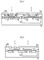
- a protective structure according to the invention can be according to FIG an output of an integrated circuit can be arranged.
- The contains a MOS transistor 1 and one as a trough resistor realized resistance 2.
- the transistor 1 is also part of an active output circuit, for example of an inverter ( Figure 3).
- the transistor is in a semiconductor substrate 3, which is p-doped, for example.
- the transistor 1 is therefore of the n-type.
- the Source doping region 4 is via a metal contact with a Supply potential VSS (ground) connected.
- a drain connection 5 of the transistor 1 is through the resistor 2 to the Output port 8 connected.
- Between the drain and Source regions 5 and 4 of transistor 1 is its gate electrode 6 arranged, which consist of a gate oxide 6a and above Polysilicon 6b is made.
- the gate electrode is electrically connectable via a metal contact 9.
- a silicide layer 10a, 10b, 10c applied on the Drain and source diffusion areas of the transistor and that The polysilicon gate is directly a silicide layer 10a, 10b, 10c applied. Through the silicide layer Switching properties of the transistor improved. It will in particular the resistance of doping regions and polysilicon reduced.
- the tub resistance 2 that between the Drain area and the output terminal 8 is switched, includes a well 13 of the n-conductivity type, each with a doping region 14, 15 of the n-line type for connection to the drain region 5 of the Transistor 1 or to the output terminal 8 and a between the connection areas 14, 15 arranged gate 16.
- a tub is a deep doping area with significantly higher Doping as the semiconductor substrate.
- Connection area 14 is connected to the drain area of the Transistor 1 connected, the connection region 15 via a metal conductor 17 with the output terminal 8.
- the silicon surfaces resistor 2, d. H. the connection areas 14, 15 and gate 16 are also with a silicide layer 11a, 11b, 11c covered, in the same process step as that Silicide layer 10a, 10b, 10c is produced.
- the transistor 1 and the resistor 2 are on the surface of the semiconductor substrate 3 or the tub 13 from a local oxide layer 18 surrounded.
- the n-channel transistor 1 is used to overvoltage pulses Connection 8, for example, from an electrostatic Discharge originate to derive to the supply potential VSS.
- the tub resistance is to be dimensioned so that the switching properties of the transistor in the inverter stage is only insignificant be influenced, the current flow in an electrostatic However, discharge is reduced so far that destruction of transistor 1 or resistor 2 excluded becomes.
- Between the connection areas 14, 15 of the Trough 13 is essentially effective as a resistance Area of the tub 13. The resistance value can be determined by the Dimensioning of the distance and the doping of the tub 13 can be set.
- gate 16 Because of that between the connecting areas 14, 15 arranged gate is the one in this area existing silicide layer 11b not directly on the Silicon surface of the tub 13 arranged. This has the silicide layer 11b has no influence on the effective Resistance value of the tub 13.
- the gate 16 is put together with the gate 6 of the transistor 1 in the same manufacturing step manufactured. As a result, there is no additional manufacturing effort necessary.
- the use of gate 16 has process engineering the advantage that its length, ie the Distance between areas 14, 15, precisely controllable is.
- the gate 16 is the longitudinal extension smallest structure that can be manufactured in a controlled manner can. The resistance value of the tub resistance 2 can therefore relatively accurate and with little space consumption will be realized.
- FIG. 2 shows an improved embodiment of the in the protective structure shown in Figure 1. Same Elements are provided with the same reference symbols.
- the drain region of transistor 1 and the drain-side connection region of the tub resistance 2 are as a coherent Doping region 20 formed.
- the funding area 20 runs across the border between tub 21 and substrate 3.
- the protective structure of FIG. 2 is also can be implemented without additional process engineering effort. Compared to the embodiment according to FIG. 1 uses less silicon area. In addition, the necessary metal conductor 12 there.
- the exemplary embodiments described so far contain as an active component an n-channel transistor that directly is realized in the p-type substrate 3.
- the invention but can also on a p-channel transistor and p-doped Semiconductor substrate can be applied.
- Such a p-channel transistor is known to be arranged in an n-well.
- the tub resistance according to the invention, between the p-type drain region of the p-channel transistor and the Output connection is switched in corresponding Realized to the resistor 2 of Figure 1.
- the gate 16 of the resistor 2 is shown in FIGS. 1, 2 as not shown connected. The gate then follows through capacitive coupling to the drain potential of transistor 1.
- connection areas of the tub and to connect the gate of resistor 2 are in the figure 3a to 3d shown.
- the output stage is from the Transistors 30, 31 together with the tub resistor and shown the gate connection of the tub according to the invention.
- the N-channel transistor 30 is at the supply potential VSS (Ground) connected, the p-channel transistor 31 with respect to of the potential VSS positive supply potential VDD.
- the gate electrodes of transistors 30, 31 are from controlled a signal to be output at the output 8.
- the gate connections of the transistors 30, 31 be connected so that the function of an inverter.
- In Figure 3a are between the Drain terminal of transistor 30 and the output terminal 8 the tub resistor 32 and the associated gate 33 effective.
- Gate 33 is not connected, but can, as mentioned above advantageously to the gate terminal of the transistor 30, the output connection or the potential VDD connected become.
- the resistor 32 acts only on the Transistor 30.
- the tub resistance 34 ( Figure 3b) and the associated Gate 35 between the drain regions of both transistors 30, 31 and the output terminal 8 switched.
- the tub resistance 34 acts here as a discrete resistor on the transistors 30, 31. This is due to the corresponding metal conductor banners to reach.
- the gate of the tub resistor 34 can remain disconnected or to the output port 8, the connection node 36 of the drainage areas of the Transistors 30, 31 or the supply potential VDD connected become.
- the tub resistance 34 dimensioned such that the switching networking the output stage is not significantly affected becomes.
- connection area of the tub of a gate instead of the connection area of the tub of a gate a local oxide corresponding to that in local oxide 18 shown in Figure 1 is arranged. Also this ensures that the silicide layer is not rests directly on the silicon surface belonging to the tub.
- the corresponding electrical equivalent circuit diagrams are shown in Figures 3c and 3d. In this case it works the tub resistance alone as ohmic resistance 37 or 38.
- the resistance either between the drain area of a switching transistor the output stage and the output connection switched be ( Figure 3c) or between the drain areas of the two p- and n-channel transistors of the output stage and the output connector ( Figure 3d). Also through this measure the ESD resistance of the output transistors Use of a silicide layer increases without additional Manufacturing steps are necessary.
- FIG. 4 is a known arrangement shown with a thick oxide transistor. Instead of A gate electrode in a MOS transistor is in the thick oxide transistor a local oxide 50 or field oxide is present. Doping regions are on both sides of the local oxide 50 51, 52 corresponding to the source and drain areas of one MOS transistor arranged. The doping region 51 is connected to the potential VSS.
- a thick oxide transistor is preferably used as an entrance protection structure, with an input terminal of an integrated circuit is protected against ESD exposure.
- FIG. 4b there is an input 60 with the gate electrodes of the transistors of an input switching stage 61 is connected via a thick oxide transistor 62 to the Potential VSS connected. This is on the input side connected doping region of the thick oxide transistor 62 through a trough resistor 63 to the input terminal 60 connected.
- a thick oxide transistor can also be used to protect an output connection be used.
- Resistor 63 is a trough resistor realized.
- the p-doped semiconductor substrate 3 introduced an n-well 53.
- the transistor-side n-connection area the tub forms with the corresponding doping region 52 of the transistor a continuous doping region.
- Another tub connection 54 is via a Metal trace 56 with the input terminal 60 of the integrated Circuit connected.
- Between the n-doping regions 52, 54 is another local oxide section 55 arranged. The oxide 55 prevents that a silicide layer immediately on the silicon surface the tub 53 rests. Thus, high local Current loads and thus local destruction of the semiconductor structure avoided.
- a thick oxide transistor can both directly in the semiconductor substrate as well as a thick oxide transistor Complementary cable type implemented in a tub become. Instead of the local oxide 55, a Transistor gate are used. The gate can be both electrical connected as well as not connected. A floating, i.e. not connected gate is special advantageous because it makes the series resistance relatively is high and therefore the ESD resistance of the thick oxide transistor is increased. Since the thick oxide transistor is not in the Switching operation is used for signal processing the high series resistance does not affect the switching operation.
- Another protective element, preferably as Input useful element for an integrated circuit is a resistance of a doping region. Usually the resistance is generated by diffusion.
- the resistance value of the diffused resistance is caused by the silicide layer applied to the silicon surface reduced. Through the realization the diffused resistance using a trough the resistance value can be set to one for ESD protection usable value can be set.
- the connection areas the well are separated by a local oxide or, according to the invention, by a gate Cut.
- MOS transistor is also used as an input protection structure by placing the drain-source path between one Input connection and a supply potential switched is.
- the MOS transistor is used to increase the ESD resistance connected in series with a trough resistor.
- FIG 5 is the supervision of an inventive Protective structure, for example according to the protective structure Figure 2 shown.
- the same elements have the same reference symbols Mistake.
- the MOS transistor 1 is included the resistor 2 shown, which is arranged in the tub 21 is. Transistor and well are shown in the vertical Extended direction.
- In the funding areas 4, 22 are the corresponding metal contacts 60 and 61, respectively for connection to the supply potential VSS or the output connection 8 shown.
- the doping region 20, which as Drain area of transistor 1 and connection area of the tub 21 is used, is formed in strips on the surface.
- the surface of the diffusion region has strips 20a to 20i, which extend from the transistor gate 6 to the gate 16 of the Pan resistance extend.
- the strips 20a to 20e are covered with a silicide layer.
- Strips 20a to 20e each have a strip-shaped area 20f to 20i of the doping region 20, which is on the surface is covered with a local oxide layer. Thereby is prevented in the stripes 20f to 20i of the doping region 20 a silicide layer on the silicon surface lies.
- the strip-like design of the surface of the doping region 20 is thus advantageously prevented that there is a current concentration during a local breakdown set to a narrowly defined breakthrough area.
- the sections 20a to 20i of the doping region 20 thus acts the tub resistance with the strip proportionally assigned resistance section.
- the interruption of the silicide layer on the surface of the Doping region 20 can have both a gate and with the local oxide layer shown in FIG. 5.
- This interruption either with a local oxide or a gate, can be on thick oxide transistors and MOS transistors when executing the tub resistance both with a local oxide layer as well as with a gate alike be applied.
- this gate can be connected to the gate 6 of the transistor 1 and optionally additionally by means of metal conductor tracks the transistor gate 6 are connected.
Landscapes
- Engineering & Computer Science (AREA)
- Power Engineering (AREA)
- Physics & Mathematics (AREA)
- Condensed Matter Physics & Semiconductors (AREA)
- General Physics & Mathematics (AREA)
- Computer Hardware Design (AREA)
- Microelectronics & Electronic Packaging (AREA)
- Semiconductor Integrated Circuits (AREA)
- Metal-Oxide And Bipolar Metal-Oxide Semiconductor Integrated Circuits (AREA)
Claims (6)
- Structure de protection vis-à-vis des décharges électrostatiques pour des circuits intégrés à semi-conducteur comprenant :(a) une borne (8) à protéger du circuit intégré ;(b) un composant (1) à semi-conducteur, qui est monté entre la borne (8) du circuit intégré et une borne pour un potentiel (VSS) d'alimentation et qui comporte une zone (5) de dopage qui peut être reliée à la borne (8) du circuit intégré ;(c) une résistance (2) qui est réalisée en zone (13) de dopage à cuvette et qui est interposée entre la zone (5) de dopage du composant (1) à semi-conducteur et la borne (8) du circuit intégré ;(d) la zone (13) de dopage à cuvette comportant une première zone (14) de dopage de borne destinée au raccordement à la zone (5) de dopage du composant (1) à semi-conducteur et une deuxième zone (15) de dopage de borne destinée au raccordement à la borne (8) du circuit intégré ;(e) une grille (16) de transistor est disposée entre les zones (14, 15) de dopage de borne et(f) la première et la deuxième zones (14, 15) de dopage de borne ont le même type de conductivité que la zone (13) de dopage de cuvette.
- Structure de protection selon la revendication 1, caractérisée en ce que la première zone (14) de dopage de borne et la zone (5) de dopage du composant (1) à semi-conducteur forment une zone (20) de dopage continue.
- Structure de protection selon la revendication 2, caractérisée en ce que la zone (20) de dopage continu comporte des bandes qui sont constituées sur la surface en siliciure et qui sont constituées alternativement de siliciure (20a, ..., 20 e) et d'une grille (20f, ..., 20i) de transistor.
- Structure de protection selon la revendication 3, caractérisée en ce que la zone (20) de dopage continu comporte sur la surface de siliciure des bandes qui sont constituées alternativement en siliciure (20a, ..., 20 e) et en un oxyde local.
- Structure de protection selon l'une des revendications 2 à 4, caractérisée en ce que le composant (1) à semi-conducteur est un transistor MOS.
- Structure de protection selon l'une des revendications 2 à 4, caractérisée en ce que le composant (1) à semi-conducteur est un transistor (50, 51, 52) à oxyde épais.
Applications Claiming Priority (2)
| Application Number | Priority Date | Filing Date | Title |
|---|---|---|---|
| DE4341170 | 1993-12-02 | ||
| DE4341170A DE4341170C2 (de) | 1993-12-02 | 1993-12-02 | ESD-Schutzstruktur für integrierte Schaltungen |
Publications (3)
| Publication Number | Publication Date |
|---|---|
| EP0656659A2 EP0656659A2 (fr) | 1995-06-07 |
| EP0656659A3 EP0656659A3 (fr) | 1996-11-13 |
| EP0656659B1 true EP0656659B1 (fr) | 2002-03-06 |
Family
ID=6504059
Family Applications (1)
| Application Number | Title | Priority Date | Filing Date |
|---|---|---|---|
| EP94119073A Expired - Lifetime EP0656659B1 (fr) | 1993-12-02 | 1994-12-02 | Structure de protection ESD pour circuit intégrés |
Country Status (2)
| Country | Link |
|---|---|
| EP (1) | EP0656659B1 (fr) |
| DE (2) | DE4341170C2 (fr) |
Families Citing this family (7)
| Publication number | Priority date | Publication date | Assignee | Title |
|---|---|---|---|---|
| DE19654927C2 (de) * | 1995-07-31 | 2003-03-06 | Mitsubishi Electric Corp | Statische Halbleiterspeichervorrichtung (SRAM) |
| JP3428240B2 (ja) * | 1995-07-31 | 2003-07-22 | 三菱電機株式会社 | 半導体記憶装置 |
| JP3717227B2 (ja) * | 1996-03-29 | 2005-11-16 | 株式会社ルネサステクノロジ | 入力/出力保護回路 |
| JP3169844B2 (ja) * | 1996-12-11 | 2001-05-28 | 日本電気株式会社 | 半導体装置 |
| JPH11126899A (ja) * | 1997-10-22 | 1999-05-11 | Mitsubishi Electric Corp | 半導体装置およびその製造方法 |
| JP3033548B2 (ja) | 1997-11-12 | 2000-04-17 | 日本電気株式会社 | 半導体装置、静電保護素子及び絶縁破壊防止方法 |
| US6587320B1 (en) | 2000-01-04 | 2003-07-01 | Sarnoff Corporation | Apparatus for current ballasting ESD sensitive devices |
Family Cites Families (6)
| Publication number | Priority date | Publication date | Assignee | Title |
|---|---|---|---|---|
| JPS5869124A (ja) * | 1981-10-20 | 1983-04-25 | Toshiba Corp | 半導体集積回路 |
| ES2055795T3 (es) * | 1988-11-22 | 1994-09-01 | At & T Corp | Separador de salida de circuito integrado que tiene proteccion de esd mejorada. |
| US5248892A (en) * | 1989-03-13 | 1993-09-28 | U.S. Philips Corporation | Semiconductor device provided with a protection circuit |
| NL8900593A (nl) * | 1989-03-13 | 1990-10-01 | Philips Nv | Halfgeleiderinrichting met een beveiligingsschakeling. |
| US5157573A (en) * | 1989-05-12 | 1992-10-20 | Western Digital Corporation | ESD protection circuit with segmented buffer transistor |
| GB2242781A (en) * | 1990-04-06 | 1991-10-09 | Koninkl Philips Electronics Nv | A semiconductor device |
-
1993
- 1993-12-02 DE DE4341170A patent/DE4341170C2/de not_active Expired - Fee Related
-
1994
- 1994-12-02 EP EP94119073A patent/EP0656659B1/fr not_active Expired - Lifetime
- 1994-12-02 DE DE59410070T patent/DE59410070D1/de not_active Expired - Lifetime
Also Published As
| Publication number | Publication date |
|---|---|
| EP0656659A2 (fr) | 1995-06-07 |
| EP0656659A3 (fr) | 1996-11-13 |
| DE4341170A1 (de) | 1995-06-08 |
| DE4341170C2 (de) | 2001-05-03 |
| DE59410070D1 (de) | 2002-04-11 |
Similar Documents
| Publication | Publication Date | Title |
|---|---|---|
| EP1019964B1 (fr) | Circuit integre a semiconducteur comportant une structure servant a la protection contre des decharges electrostatiques | |
| DE102011054700B4 (de) | Halbleiter-ESD-Bauelement und Verfahren | |
| DE102010000531B4 (de) | Halbleiterbauelement, elektronische Komponente und Verfahren zur Herstellung eines Halbleiterbauelements | |
| DE19651247C2 (de) | Eingabe/Ausgabeschutzschaltung | |
| DE69631940T2 (de) | Halbleitervorrichtung | |
| DE2559360A1 (de) | Halbleiterbauteil mit integrierten schaltkreisen | |
| DE4110369C2 (de) | MOS-Halbleiterbauelement | |
| DE69834315T2 (de) | Integrierte Schaltung mit einem VDMOS-Transistor, der gegen Überspannungen zwischen Source und Gate geschützt ist | |
| DE19654163B4 (de) | Schutzvorrichtung für eine Halbleiterschaltung | |
| DE102013101705A1 (de) | ESD-Vorrichtungen mit Halbleiterfinnen | |
| EP0538507B1 (fr) | Circuit de protection pour contacts de connexion de circuits intégrés monolithiques | |
| DE2047166B2 (de) | Integrierte Halbleiteranordnung | |
| DE7148143U (de) | Spannungsgesteuerte cmos-gatterschutz-diode | |
| DE2226613A1 (de) | Halbleiterbauelement | |
| DE102010005715B4 (de) | Transistoranordnung als ESD-Schutzmaßnahme | |
| DE102005011348B4 (de) | Halbleitervorrichtung | |
| DE2832154C2 (fr) | ||
| DE4120394A1 (de) | Monolithisch integrierte schaltungsanordnung | |
| DE102004059627B4 (de) | Halbleitervorrichtung mit einem Hochpotentialinselbereich | |
| DE10216015A1 (de) | Überspannungsschutzschaltung | |
| EP0656659B1 (fr) | Structure de protection ESD pour circuit intégrés | |
| DE2030423A1 (de) | Integrierte Metall Oxid Halbleiter schaltung mit einer Schutzschaltung gegen Spannungsstoßc | |
| DE2736324C2 (de) | Logische Verknüpfungsschaltung | |
| DE102008047850B4 (de) | Halbleiterkörper mit einer Schutzstruktur und Verfahren zum Herstellen derselben | |
| DE19936636A1 (de) | Schutzstruktur für eine integrierte Halbleiterschaltung zum Schutz vor elektrostatischer Entladung |
Legal Events
| Date | Code | Title | Description |
|---|---|---|---|
| PUAI | Public reference made under article 153(3) epc to a published international application that has entered the european phase |
Free format text: ORIGINAL CODE: 0009012 |
|
| AK | Designated contracting states |
Kind code of ref document: A2 Designated state(s): DE FR IT NL |
|
| PUAL | Search report despatched |
Free format text: ORIGINAL CODE: 0009013 |
|
| AK | Designated contracting states |
Kind code of ref document: A3 Designated state(s): DE FR IT NL |
|
| 17P | Request for examination filed |
Effective date: 19970514 |
|
| 17Q | First examination report despatched |
Effective date: 19981112 |
|
| GRAG | Despatch of communication of intention to grant |
Free format text: ORIGINAL CODE: EPIDOS AGRA |
|
| GRAG | Despatch of communication of intention to grant |
Free format text: ORIGINAL CODE: EPIDOS AGRA |
|
| GRAH | Despatch of communication of intention to grant a patent |
Free format text: ORIGINAL CODE: EPIDOS IGRA |
|
| RAP1 | Party data changed (applicant data changed or rights of an application transferred) |
Owner name: INFINEON TECHNOLOGIES AG |
|
| GRAH | Despatch of communication of intention to grant a patent |
Free format text: ORIGINAL CODE: EPIDOS IGRA |
|
| GRAA | (expected) grant |
Free format text: ORIGINAL CODE: 0009210 |
|
| AK | Designated contracting states |
Kind code of ref document: B1 Designated state(s): DE FR IT NL |
|
| REF | Corresponds to: |
Ref document number: 59410070 Country of ref document: DE Date of ref document: 20020411 |
|
| ET | Fr: translation filed | ||
| PLBE | No opposition filed within time limit |
Free format text: ORIGINAL CODE: 0009261 |
|
| STAA | Information on the status of an ep patent application or granted ep patent |
Free format text: STATUS: NO OPPOSITION FILED WITHIN TIME LIMIT |
|
| 26N | No opposition filed |
Effective date: 20021209 |
|
| PGFP | Annual fee paid to national office [announced via postgrant information from national office to epo] |
Ref country code: NL Payment date: 20061215 Year of fee payment: 13 |
|
| PGFP | Annual fee paid to national office [announced via postgrant information from national office to epo] |
Ref country code: IT Payment date: 20061231 Year of fee payment: 13 |
|
| NLV4 | Nl: lapsed or anulled due to non-payment of the annual fee |
Effective date: 20080701 |
|
| PG25 | Lapsed in a contracting state [announced via postgrant information from national office to epo] |
Ref country code: NL Free format text: LAPSE BECAUSE OF NON-PAYMENT OF DUE FEES Effective date: 20080701 |
|
| PG25 | Lapsed in a contracting state [announced via postgrant information from national office to epo] |
Ref country code: IT Free format text: LAPSE BECAUSE OF NON-PAYMENT OF DUE FEES Effective date: 20071202 |
|
| PGFP | Annual fee paid to national office [announced via postgrant information from national office to epo] |
Ref country code: DE Payment date: 20140214 Year of fee payment: 20 |
|
| PGFP | Annual fee paid to national office [announced via postgrant information from national office to epo] |
Ref country code: FR Payment date: 20131220 Year of fee payment: 20 |
|
| REG | Reference to a national code |
Ref country code: DE Ref legal event code: R071 Ref document number: 59410070 Country of ref document: DE |