EP0650196A2 - Semiconductor integrated circuit device and method of producing the same using master slice approach - Google Patents
Semiconductor integrated circuit device and method of producing the same using master slice approach Download PDFInfo
- Publication number
- EP0650196A2 EP0650196A2 EP94119969A EP94119969A EP0650196A2 EP 0650196 A2 EP0650196 A2 EP 0650196A2 EP 94119969 A EP94119969 A EP 94119969A EP 94119969 A EP94119969 A EP 94119969A EP 0650196 A2 EP0650196 A2 EP 0650196A2
- Authority
- EP
- European Patent Office
- Prior art keywords
- wiring layer
- cell region
- input
- region
- wiring
- Prior art date
- Legal status (The legal status is an assumption and is not a legal conclusion. Google has not performed a legal analysis and makes no representation as to the accuracy of the status listed.)
- Withdrawn
Links
Images


Classifications
-
- H—ELECTRICITY
- H10—SEMICONDUCTOR DEVICES; ELECTRIC SOLID-STATE DEVICES NOT OTHERWISE PROVIDED FOR
- H10D—INORGANIC ELECTRIC SEMICONDUCTOR DEVICES
- H10D84/00—Integrated devices formed in or on semiconductor substrates that comprise only semiconducting layers, e.g. on Si wafers or on GaAs-on-Si wafers
- H10D84/90—Masterslice integrated circuits
- H10D84/903—Masterslice integrated circuits comprising field effect technology
- H10D84/907—CMOS gate arrays
-
- H—ELECTRICITY
- H10—SEMICONDUCTOR DEVICES; ELECTRIC SOLID-STATE DEVICES NOT OTHERWISE PROVIDED FOR
- H10D—INORGANIC ELECTRIC SEMICONDUCTOR DEVICES
- H10D84/00—Integrated devices formed in or on semiconductor substrates that comprise only semiconducting layers, e.g. on Si wafers or on GaAs-on-Si wafers
- H10D84/01—Manufacture or treatment
-
- H—ELECTRICITY
- H10—SEMICONDUCTOR DEVICES; ELECTRIC SOLID-STATE DEVICES NOT OTHERWISE PROVIDED FOR
- H10D—INORGANIC ELECTRIC SEMICONDUCTOR DEVICES
- H10D89/00—Aspects of integrated devices not covered by groups H10D84/00 - H10D88/00
- H10D89/10—Integrated device layouts
-
- H10W20/43—
Definitions
- the present invention relates to a technique of utilizing a master slice approach and, more particularly, to a semiconductor integrated circuit device and a method of producing the device using the master slice approach.
- a semiconductor integrated circuit or large scale integrated circuit device produced through the master slice approach is hereinafter referred to as a master slice type LSI device.
- the master slice approach generally comprises a first process of forming a master chip and a second process of forming a desired wiring pattern on the master chip.
- a basic cell region including a plurality of basic cells, each consisting of a predetermined number of transistors, is formed together with an input/output (I/O) cell region on a chip using a common and fixed pattern mask.
- the second process is carried out in accordance with a specification or conditions demanded by a user and includes a plurality of steps.
- the second process normally includes four steps of: forming contact holes in a first insulation layer formed on the master chip; forming thereon a first wiring layer; forming through holes in a second insulation layer formed thereon; and forming thereon a second wiring layer so as to contact the first wiring layer via through holes. Therefore, four pattern masks corresponding to the contact hole, first wiring layer, through hole and second wiring layer are required to constitute a given circuit in the basic cell region.
- This one custom mask approach is a method of forming a wiring pattern on the master chip using one layer custom mask (wiring pattern mask according to a user's specification).
- wiring pattern mask according to a user's specification.
- the wiring pattern mask can be made common to a plurality of master slice type LSI devices, it becomes possible to easily realize the reduction of the turnaround time and the simplification of the process.
- An embodiment of the present invention may provide a master slice type LSI device and a method of producing the device which can greatly reduce a turnaround time.
- An embodiment of the present invention may apply the one custom mask approach to an I/O cell region of a master chip, thereby producing a desired master slice type LSI device easily and in a short period.
- a semiconductor integrated circuit device comprising: a master chip including a basic cell region having a plurality of basic cell arrays arranged thereon, and an input/output cell region having a plurality of input/output cells arranged along the periphery of the basic cell region; a first wiring layer formed on the basic cell region and the input/output cell region via a first insulation layer having contact holes at predetermined positions; and a second wiring layer formed on the first wiring layer via a second insulation layer having through holes at predetermined positions; wherein the first wiring layer includes fixed wirings in a region corresponding to the input/output cell region, and the second wiring layer includes wirings programmed in accordance with conditions of a given circuit applied to the input/output cell region in a region corresponding to the input/output region.
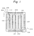
- Figure 1 schematically illustrates a whole constitution of a master chip in the master slice type LSI device of the present invention.
- reference 201 denotes a basic cell region, which is formed on the central region of a master chip 203 and includes a plurality of basic cell arrays 206 extending along a Y direction with a predetermined spacing therebetween.
- Each of the basic cells 204, 205, and each pair of basic cells are parallelly disposed along an X direction perpendicular to the Y direction. Namely, a plurality of basic cells 204, 205 are arranged in the form of a so-called double column structure on the master chip.
- Reference 202 denotes an I/O cell region, which is formed along the periphery of the master chip 203 and includes a plurality of I/O cells 207. A concrete constitution of each I/O cell will be described later.
- Reference 208 denotes a wiring channel region formed between adjacent basic cell arrays 206.
- FIG. 2 illustrates a portion of the basic cell array shown in Fig. 1.
- each basic cell 1 (corresponding to the basic cell 204 or 205 in Fig. 1) is constituted by a pair of p-channel transistors Qp connected in series and a pair of n-channel transistors Qn connected in series.
- One of the p-channel transistors is constituted by a gate electrode 2 and p-channel impurity regions 4, 5 serving as a source/drain, and another is constituted by a gate electrode 3 and p-type impurity regions 5, 6 serving as a source/drain.
- one of the n-channel transistors is constituted by a gate electrode 2 and n-type impurity regions 7, 8 serving as a source/drain, and another is constituted by a gate electrode 3 and p-type impurity regions 8, 9 serving as a source/drain.
- Reference 10 denotes a separation region for separating a region on which p-channel transistors are formed from a region on which n-channel transistors are formed.
- References 11 to 16 denote lead portions used for connecting gate electrodes 2, 3 to each portion of a given logic circuit or gate, which are constituted by a portion of the gate electrodes and formed in each end portion and each central portion, respectively.
- the lead portions 11 to 16 are hereinafter referred to as gate electrode lead portions.
- the gate electrode lead portions 11 to 16 and the gate electrodes 2, 3 are composed of, for example, polysilicon.
- reference B1 indicates a basic block in which the logic circuit or gate is formed, and which is constituted by a pair of basic cells 1 parallely disposed along a longitudinal (Y) direction.
- Reference B2 indicates a basic block as well, which is constituted by a single basic cell 1.
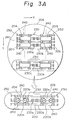
- Figures 3A to 3C illustrate constitutions of main parts of the master chip shown in Fig. 1.
- references 220a, 220b denote transistors of CMOS structure and correspond to the p-channel transistor Qp and n-channel transistor Qn shown in Fig. 2, respectively. Accordingly, each of the basic cells 204, 205 is constituted by two pairs of CMOS transistors 220a, 220b.
- Reference 230 denotes a cell-to-cell wiring region, which is extending along the Y direction between adjacent basic cells 204, 205 disposed along the X direction. A portion of the cell-to-cell wiring region 230 is included in the wiring channel region 208 (see Fig. 1).
- Reference 240 denotes a bypass wiring region, which is formed between adjacent basic cells 204 (205) disposed along the Y direction, and extending along the X direction. Namely, the bypass wiring region 240 and the basic cell 204 (205) are alternately arranged along the Y direction
- Reference 250 denotes an end portion wiring region, which is formed in an end portion of the basic cell array 206 and extending along the Y direction. Namely, a pair of end portion wiring region 250 are formed with respect to one basic cell array 206.
- the cell-to-cell wiring region 230, bypass wiring region 240 and end portion wiring region 250 include a plurality of wirings of a predetermined length, respectively, and a connection of wirings between each region is not effected.
- the cell-to-cell wiring region 230 comprises a short wiring region 230a and a long wiring region 230b.
- the short wiring region 230a includes a plurality of short wirings extending along the X direction, which are divided into a plurality of portions along the X direction in a region between adjacent basic cells 204, 205 disposed along the X direction, and arranged at a predetermined spacing in the Y direction.
- the long wiring region 230b includes a plurality of long wirings, which are continuously extending along the X direction in a region between adjacent bypass wiring regions 240 disposed along the X direction.
- the number of the wirings in the long wiring region 230b is the same as that in the bypass wiring region 240.
- Each of the long wirings is formed such that an end portion thereof faces that of each of the wirings in the bypass wiring region 240 and extends internally from an end portion of the basic cell 204, 205.
- the wiring channel region 208 includes a plurality of wirings 208a of a predetermined length extending along the X direction, which are divided into a plurality of portions along the X direction and arranged at a predetermined space in the Y direction.
- the wiring channel region 208 is formed so as to be wider than the cell-to-cell wiring region 230 (in the present example, twice or more). The distance between each contact hole provided in the region of the wirings 208a is selected such that one vertical wiring formed in the second wiring layer can pass therethrough.
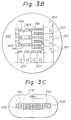
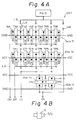
- Figures 4A and 4B illustrate the mounting pattern of each of the I/O cells 207 shown in Fig. 3B.
- the I/O cell 207 includes three diffusion regions for MOS transistors. These diffusion regions are constituted by the following constituent elements: n-channel MOS transistors TN1 ⁇ TN6, e.g., for an output buffer; a p-channel MOS transistor TPU functioning as an input pull-up resistor; and an n-channel MOS transistor TPD functioning as an pull-down resistor. Each transistor is constituted by a gate G and a source/drain S/D, as shown in Fig. 4B.
- each transistor is connected via the contact hole NA to the first wiring layer (wirings) LA, and the first wiring layer (wirings) LA is connected via the through hole NB to the second wiring layer (wirings) LB.
- the second wiring layer (wirings) LB is formed using a custom pattern mask according to the user's specification, in another process different from the process of forming basic cell regions.
- reference PAD denotes a bonding pad; reference Vcc a power supply line; reference GND a ground line; reference IN an input buffer internal terminal; reference CI a clock buffer internal terminal; reference OP an output buffer internal terminal for p-channel MOS transistors; and reference ON an output buffer internal terminal for n-channel MOS transistors. Since the relation of connection between each element is apparent from Fig. 4A, its explanation is omitted.
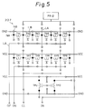
- Figure 5 illustrates an equivalent circuit, symbolically showing transistor diffusion regions TN1 ⁇ TN6, TP1 ⁇ TP6, TPU and TPD in Fig. 4A.
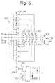
- Fig. 6 illustrates an equivalent circuit of the pattern shown in Fig. 4A, together with program points.
- Each of the program points is shown by a block PP indicated by a dotted line, and corresponds to a region in which a connection between wirings is effected in the second wiring layer in accordance with demanded conditions of a given circuit.
- the portion surrounded by a dot-dash line indicates an input protection circuit.
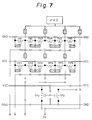
- Figure 7 illustrates a pattern diagram of an input buffer circuit as a first application
- Fig. 8 illustrates an equivalent circuit thereof.
- connection portion (program point) formed by the custom pattern mask is indicated by a hatched portion in Fig. 7, and by a thick solid line in Fig. 8. Note, the manner of the indication of connection portion (program point) is common to other applications described later.
- a signal input through the pad PAD is directly output to the terminal IN.
- the p-channel MOS transistors TP1 ⁇ TP6, each being brought to an OFF state, and the n-channel MOS transistors TN1 ⁇ TN6, each being brought to an OFF state are connected to each other.
- a PN junction between the source and drain of the corresponding pair of p-channel and n-channel MOS transistors constitutes a parasitic diode, which functions as a protection circuit against static electricity.
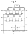
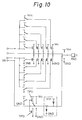
- Figure 9 illustrates a pattern diagram of an input buffer circuit with a pull-up resistor as a second application
- Fig. 10 illustrates an equivalent circuit thereof
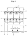
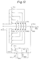
- Fig. 11 illustrates a pattern diagram of an input buffer circuit with a pull-down resistor as a third application
- Fig. 12 illustrates an equivalent circuit thereof.
- the MOS transistor TPU in Figs. 9, 10 is connected so as to be brought to a normally-ON state and, accordingly, employed as a pull-up resistor.
- the MOS transistor TPD in Figs. 11, 12 is connected so as to be brought to a normally-ON state and, accordingly, employed as a pull-down resistor.
- Each resistance value of the pull-up resistor and pull-down resistor is appropriately selected according to the size of each transistor.
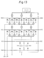
- Figure 13 illustrates a pattern diagram of an output buffer circuit as a fourth application
- Fig. 14 illustrates an equivalent circuit thereof.
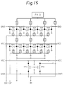
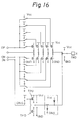
- Figure 15 illustrates a pattern diagram of a bidirectional buffer circuit as a fifth application
- Fig. 16 illustrates an equivalent circuit thereof.
- the illustrated bidirectional buffer circuit is a combination of the input buffer Circuit shown in Figs. 7, 8 and the output buffer circuit shown in Figs. 13, 14.
- the pull-up resistor or pull-down resistor can be provided with the bidirectional buffer circuit, if necessary.
- Figure 17 illustrates a pattern diagram of a clock buffer circuit as a sixth application
- Fig. 18 illustrates an equivalent circuit thereof.
- Figs. 17 and 18 output signals from internal cells are fed through the terminals OP and ON, and a clock signal is fed through the terminal CI to the internal cells. Since the clock buffer circuit drives the internal cells of heavy load, its scale or size inevitably becomes large. As a result, it is difficult to constitute the clock buffer circuit by the internal cells. Contrary to this, since the clock buffer circuit according to the present embodiment is constituted by I/O cells provided in the periphery of the chip, it is possible to prevent an increase in the size of the chip.
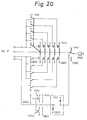
- Figure 19 illustrates a pattern diagram of a power voltage supply circuit as a seventh application
- Fig. 20 illustrates an equivalent circuit thereof
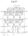
- Fig. 21 illustrates a pattern diagram of a ground voltage supply circuit as an eighth application
- Fig. 22 illustrates an equivalent circuit thereof.
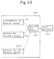
- the illustrated designing apparatus 400 comprises a fundamental mask pattern memory means 401, a wiring mask pattern memory means 402 and a pattern synthesizing means 403.
- the fundamental mask pattern memory means 401 stores two kinds of fundamental mask pattern information.
- One is a first fundamental mask pattern information consisting of four kinds of mask patterns, i.e., contact holes NA, first wiring layer (wirings) LA, through holes NB and second wiring layer (wirings) LB, necessary for forming a demanded connection between constituent elements in the basic cell region.
- Another is a second fundamental mask pattern information consisting of four kinds of mask patterns, i.e., contact holes NA, first wiring layer (wirings) LA, through holes NB and second wiring layer (wirings) LB, necessary for forming a demanded connection between constituent elements in the I/O circuits provided on the master chip.
- the wiring mask pattern memory means 402 stores two kinds of wiring mask pattern information. One is a first plurality of wiring mask patterns with respect to one wiring layer to be combined on the fundamental mask patterns, and another is a second plurality of wiring mask patterns necessary for forming one wiring layer in the program points in accordance with the kind of the I/O circuit to constitute the connection portions.
- the I/O circuit corresponds to the input buffer circuit, output buffer circuit, bidirectional buffer circuit, power voltage supply circuit or the like, as shown in Figs. 7 to 22.
- the mask pattern of the internal circuit (basic cells) in the LSI is generated based on the first fundamental mask pattern information stored in the fundamental mask pattern memory means 401 and the first wiring mask pattern information stored in the wiring mask pattern memory means 402.
- the mask pattern of the I/O circuit in the LSI is generated based on the second fundamental mask pattern information and the second wiring mask pattern information.
- the second fundamental mask pattern information and the second wiring mask pattern information corresponding to the kind of the I/O circuit are read out by the pattern synthesizing means 403, where both groups of pattern information are synthesized to generate the mask pattern 404 of the I/O circuit.
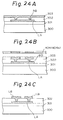
- the method of producing the master slice type LSI device roughly classifying, includes the steps of forming the basic cell region 201 together with the I/O cell regions 202 (see Fig. 1) and forming the wiring pattern using a custom mask on the cell regions.
- the basic cell regions and I/O cell regions are produced by: forming an insulation layer 301 consisting of silicon oxide and including contact holes NA (not shown) on a semiconductor substrate 300; forming thereon the first wiring layer LA by aluminium (Al) evaporation; forming thereon an insulation layer 302 consisting of silicon oxide; forming through holes NB in the insulation layer 302 so that they contact the first wiring layer LA; and forming thereon a conduction layer 303.
- the mask pattern (including the mask pattern 404 of the I/O circuit) is designed by the designing apparatus 400 (see Fig. 23) in accordance with the user's specification and then a desired wiring patterning is effected on the conduction layer 303 by an etching process using the designed mask pattern (see Fig. 24B).
- a desired second wiring layer LB is formed as shown in Fig. 24C, and the master slice type LSI device according to the user's specification can be produced.
Landscapes
- Design And Manufacture Of Integrated Circuits (AREA)
- Semiconductor Integrated Circuits (AREA)
Applications Claiming Priority (7)
| Application Number | Priority Date | Filing Date | Title |
|---|---|---|---|
| JP100631/88 | 1988-04-22 | ||
| JP63100631A JP2526269B2 (ja) | 1988-04-22 | 1988-04-22 | マスタスライス方法 |
| JP63180953A JPH0230163A (ja) | 1988-07-20 | 1988-07-20 | マスタスライス型半導体集積回路装置およびその製造方法 |
| JP63180954A JPH0230164A (ja) | 1988-07-20 | 1988-07-20 | マスタスライス型半導体集積回路装置およびその製造方法 |
| JP180953/88 | 1988-07-20 | ||
| JP180954/88 | 1988-07-20 | ||
| EP89303912A EP0338817B1 (en) | 1988-04-22 | 1989-04-20 | Master slice semiconductor integrated circuit device |
Related Parent Applications (2)
| Application Number | Title | Priority Date | Filing Date |
|---|---|---|---|
| EP89303912.3 Division | 1989-04-20 | ||
| EP89303912A Division EP0338817B1 (en) | 1988-04-22 | 1989-04-20 | Master slice semiconductor integrated circuit device |
Publications (2)
| Publication Number | Publication Date |
|---|---|
| EP0650196A2 true EP0650196A2 (en) | 1995-04-26 |
| EP0650196A3 EP0650196A3 (esLanguage) | 1995-05-10 |
Family
ID=27309268
Family Applications (2)
| Application Number | Title | Priority Date | Filing Date |
|---|---|---|---|
| EP94119969A Withdrawn EP0650196A2 (en) | 1988-04-22 | 1989-04-20 | Semiconductor integrated circuit device and method of producing the same using master slice approach |
| EP89303912A Expired - Lifetime EP0338817B1 (en) | 1988-04-22 | 1989-04-20 | Master slice semiconductor integrated circuit device |
Family Applications After (1)
| Application Number | Title | Priority Date | Filing Date |
|---|---|---|---|
| EP89303912A Expired - Lifetime EP0338817B1 (en) | 1988-04-22 | 1989-04-20 | Master slice semiconductor integrated circuit device |
Country Status (4)
| Country | Link |
|---|---|
| US (1) | US5506162A (esLanguage) |
| EP (2) | EP0650196A2 (esLanguage) |
| KR (1) | KR920008419B1 (esLanguage) |
| DE (1) | DE68929068T2 (esLanguage) |
Families Citing this family (9)
| Publication number | Priority date | Publication date | Assignee | Title |
|---|---|---|---|---|
| US5315130A (en) * | 1990-03-30 | 1994-05-24 | Tactical Fabs, Inc. | Very high density wafer scale device architecture |
| US5252507A (en) * | 1990-03-30 | 1993-10-12 | Tactical Fabs, Inc. | Very high density wafer scale device architecture |
| US5691218A (en) * | 1993-07-01 | 1997-11-25 | Lsi Logic Corporation | Method of fabricating a programmable polysilicon gate array base cell structure |
| US6242767B1 (en) | 1997-11-10 | 2001-06-05 | Lightspeed Semiconductor Corp. | Asic routing architecture |
| KR100313280B1 (ko) | 1999-10-25 | 2001-11-07 | 한신혁 | 반도체 장치의 전도배선 마스크 제조방법 |
| US6613611B1 (en) | 2000-12-22 | 2003-09-02 | Lightspeed Semiconductor Corporation | ASIC routing architecture with variable number of custom masks |
| US6885043B2 (en) * | 2002-01-18 | 2005-04-26 | Lightspeed Semiconductor Corporation | ASIC routing architecture |
| JP2006156929A (ja) * | 2004-04-19 | 2006-06-15 | Fujitsu Ltd | 半導体集積回路及びその設計方法 |
| US8097918B2 (en) * | 2009-08-14 | 2012-01-17 | Infineon Technologies Ag | Semiconductor arrangement including a load transistor and sense transistor |
Family Cites Families (25)
| Publication number | Priority date | Publication date | Assignee | Title |
|---|---|---|---|---|
| US3835530A (en) * | 1967-06-05 | 1974-09-17 | Texas Instruments Inc | Method of making semiconductor devices |
| US3702025A (en) * | 1969-05-12 | 1972-11-07 | Honeywell Inc | Discretionary interconnection process |
| US3861023A (en) * | 1973-04-30 | 1975-01-21 | Hughes Aircraft Co | Fully repairable integrated circuit interconnections |
| JPS57133712A (en) * | 1981-02-12 | 1982-08-18 | Fujitsu Ltd | Constituting method of delay circuit in master slice ic |
| JPS57211248A (en) * | 1981-06-22 | 1982-12-25 | Hitachi Ltd | Semiconductor integrated circuit device |
| EP0074805B2 (en) * | 1981-09-10 | 1992-03-11 | Fujitsu Limited | Semiconductor integrated circuit comprising a semiconductor substrate and interconnecting layers |
| JPS5851538A (ja) * | 1981-09-24 | 1983-03-26 | Hitachi Ltd | 半導体集積回路装置 |
| JPS5851537A (ja) * | 1981-09-24 | 1983-03-26 | Ricoh Co Ltd | マスタスライスチツプ |
| JPS58200570A (ja) * | 1982-05-19 | 1983-11-22 | Hitachi Ltd | 半導体集積回路装置 |
| GB2122809B (en) * | 1982-06-01 | 1985-10-02 | Standard Telephones Cables Ltd | Integrated circuit interconnection bus structure |
| DE3238311A1 (de) * | 1982-10-15 | 1984-04-19 | Siemens AG, 1000 Berlin und 8000 München | Integrierte halbleiterschaltung in gate-array-technik |
| US4568961A (en) * | 1983-03-11 | 1986-02-04 | Rca Corporation | Variable geometry automated universal array |
| JPS59204254A (ja) * | 1983-05-06 | 1984-11-19 | Sumitomo Electric Ind Ltd | 多層配線マスタスライスicの製造方法 |
| JPS59220940A (ja) * | 1983-05-31 | 1984-12-12 | Toshiba Corp | 電子ビ−ムによる半導体装置の内部動作電圧波形の測定方法 |
| US4617193A (en) * | 1983-06-16 | 1986-10-14 | Digital Equipment Corporation | Planar interconnect for integrated circuits |
| JPS6022337A (ja) * | 1983-07-19 | 1985-02-04 | Toshiba Corp | 半導体集積回路 |
| JPS6065547A (ja) * | 1983-09-20 | 1985-04-15 | Sharp Corp | 半導体装置 |
| JPH0828480B2 (ja) * | 1983-09-30 | 1996-03-21 | 富士通株式会社 | 半導体集積回路装置 |
| JPS60144956A (ja) * | 1984-01-06 | 1985-07-31 | Oki Electric Ind Co Ltd | 半導体装置の製造方法 |
| US4613941A (en) * | 1985-07-02 | 1986-09-23 | The United States Of America As Represented By The Secretary Of The Army | Routing method in computer aided customization of a two level automated universal array |
| DE3718598A1 (de) * | 1986-06-04 | 1987-12-10 | Mitsubishi Electric Corp | Halbleiteranordnung |
| JPS63275138A (ja) * | 1987-05-06 | 1988-11-11 | Nec Corp | 集積回路 |
| US5185283A (en) * | 1987-10-22 | 1993-02-09 | Matsushita Electronics Corporation | Method of making master slice type integrated circuit device |
| EP0314376B1 (en) * | 1987-10-22 | 1995-01-04 | Matsushita Electronics Corporation | Master slice type integrated circuit device and method of using it |
| JPH02247943A (ja) * | 1989-03-20 | 1990-10-03 | Toshiba Corp | カラー受像管用シャドウマスクの洗浄方法 |
-
1989
- 1989-04-20 EP EP94119969A patent/EP0650196A2/en not_active Withdrawn
- 1989-04-20 EP EP89303912A patent/EP0338817B1/en not_active Expired - Lifetime
- 1989-04-20 DE DE68929068T patent/DE68929068T2/de not_active Expired - Fee Related
- 1989-04-22 KR KR1019890005315A patent/KR920008419B1/ko not_active Expired
-
1995
- 1995-05-15 US US08/441,011 patent/US5506162A/en not_active Expired - Fee Related
Also Published As
| Publication number | Publication date |
|---|---|
| DE68929068D1 (de) | 1999-10-14 |
| EP0338817B1 (en) | 1999-09-08 |
| DE68929068T2 (de) | 1999-12-23 |
| KR890016667A (ko) | 1989-11-29 |
| EP0650196A3 (esLanguage) | 1995-05-10 |
| KR920008419B1 (ko) | 1992-09-28 |
| EP0338817A3 (en) | 1992-05-06 |
| US5506162A (en) | 1996-04-09 |
| EP0338817A2 (en) | 1989-10-25 |
Similar Documents
| Publication | Publication Date | Title |
|---|---|---|
| EP0280236B1 (en) | Method of manufacturing an insulated-gate semicustom integrated circuit | |
| US20030178648A1 (en) | Gate array core cell for VLSI ASIC devices | |
| EP0080361B1 (en) | Complementary metal-oxide semiconductor integrated circuit device of master slice type | |
| EP0093003B1 (en) | Gate array large scale integrated circuit devices | |
| US4525809A (en) | Integrated circuit | |
| JPH0369141A (ja) | セミカスタム半導体集積回路 | |
| JPH03165061A (ja) | 半導体集積回路装置 | |
| US4771327A (en) | Master-slice integrated circuit having an improved arrangement of transistor elements for simplified wirings | |
| US4992845A (en) | Semiconductor integrated circuit device having input/output buffer cells each comprising a plurality of transistor regions arranged in a single line | |
| EP0650196A2 (en) | Semiconductor integrated circuit device and method of producing the same using master slice approach | |
| JPS58182242A (ja) | 半導体集積回路装置 | |
| US5206184A (en) | Method of making single layer personalization | |
| KR100269494B1 (ko) | Soi·cmos 기술을 이용한 소형 반도체 장치 | |
| US5434436A (en) | Master-slice type semiconductor integrated circuit device having multi-power supply voltage | |
| EP0347332B1 (en) | Method of forming semiconductor integrated circuit using master slice approach | |
| EP0092176B1 (en) | Basic cell for integrated-circuit gate arrays | |
| US4942447A (en) | Borderless master slice CMOS device | |
| JP2000223575A (ja) | 半導体装置の設計方法、半導体装置および半導体装置の製造方法 | |
| US5168342A (en) | Semiconductor integrated circuit device and manufacturing method of the same | |
| EP0344055B1 (en) | Semiconductor integrated circuit device | |
| EP0349294B1 (en) | I/o cells in semiconductor integrated circuits | |
| EP0113828A2 (en) | Master slice semiconductor chip having a new multi-function FET cell | |
| JPH0230163A (ja) | マスタスライス型半導体集積回路装置およびその製造方法 | |
| EP0422930A2 (en) | Semiconductor integrated circuit devices | |
| JPS6135535A (ja) | マスタ−スライス集積回路装置 |
Legal Events
| Date | Code | Title | Description |
|---|---|---|---|
| PUAI | Public reference made under article 153(3) epc to a published international application that has entered the european phase |
Free format text: ORIGINAL CODE: 0009012 |
|
| PUAL | Search report despatched |
Free format text: ORIGINAL CODE: 0009013 |
|
| AC | Divisional application: reference to earlier application |
Ref document number: 338817 Country of ref document: EP |
|
| AK | Designated contracting states |
Kind code of ref document: A2 Designated state(s): DE FR GB |
|
| AK | Designated contracting states |
Kind code of ref document: A3 Designated state(s): DE FR GB |
|
| RHK1 | Main classification (correction) |
Ipc: H01L 27/02 |
|
| 17P | Request for examination filed |
Effective date: 19950927 |
|
| 17Q | First examination report despatched |
Effective date: 19970207 |
|
| STAA | Information on the status of an ep patent application or granted ep patent |
Free format text: STATUS: THE APPLICATION IS DEEMED TO BE WITHDRAWN |
|
| 18D | Application deemed to be withdrawn |
Effective date: 19970819 |