EP0645950B1 - Verbindungsteil eines Schaltungssubstrats und Verfahren zur Herstellung mehrschichtiger Schaltungssubstrate unter Verwendung dieses Teils - Google Patents
Verbindungsteil eines Schaltungssubstrats und Verfahren zur Herstellung mehrschichtiger Schaltungssubstrate unter Verwendung dieses Teils Download PDFInfo
- Publication number
- EP0645950B1 EP0645950B1 EP19940114796 EP94114796A EP0645950B1 EP 0645950 B1 EP0645950 B1 EP 0645950B1 EP 19940114796 EP19940114796 EP 19940114796 EP 94114796 A EP94114796 A EP 94114796A EP 0645950 B1 EP0645950 B1 EP 0645950B1
- Authority
- EP
- European Patent Office
- Prior art keywords
- connecting member
- base material
- holes
- porous base
- circuit substrate
- Prior art date
- Legal status (The legal status is an assumption and is not a legal conclusion. Google has not performed a legal analysis and makes no representation as to the accuracy of the status listed.)
- Expired - Lifetime
Links
Images


Classifications
-
- H—ELECTRICITY
- H05—ELECTRIC TECHNIQUES NOT OTHERWISE PROVIDED FOR
- H05K—PRINTED CIRCUITS; CASINGS OR CONSTRUCTIONAL DETAILS OF ELECTRIC APPARATUS; MANUFACTURE OF ASSEMBLAGES OF ELECTRICAL COMPONENTS
- H05K3/00—Apparatus or processes for manufacturing printed circuits
- H05K3/46—Manufacturing multilayer circuits
- H05K3/4611—Manufacturing multilayer circuits by laminating two or more circuit boards
- H05K3/4614—Manufacturing multilayer circuits by laminating two or more circuit boards the electrical connections between the circuit boards being made during lamination
- H05K3/462—Manufacturing multilayer circuits by laminating two or more circuit boards the electrical connections between the circuit boards being made during lamination characterized by laminating only or mainly similar double-sided circuit boards
-
- H—ELECTRICITY
- H01—ELECTRIC ELEMENTS
- H01R—ELECTRICALLY-CONDUCTIVE CONNECTIONS; STRUCTURAL ASSOCIATIONS OF A PLURALITY OF MUTUALLY-INSULATED ELECTRICAL CONNECTING ELEMENTS; COUPLING DEVICES; CURRENT COLLECTORS
- H01R12/00—Structural associations of a plurality of mutually-insulated electrical connecting elements, specially adapted for printed circuits, e.g. printed circuit boards [PCB], flat or ribbon cables, or like generally planar structures, e.g. terminal strips, terminal blocks; Coupling devices specially adapted for printed circuits, flat or ribbon cables, or like generally planar structures; Terminals specially adapted for contact with, or insertion into, printed circuits, flat or ribbon cables, or like generally planar structures
- H01R12/50—Fixed connections
- H01R12/51—Fixed connections for rigid printed circuits or like structures
- H01R12/52—Fixed connections for rigid printed circuits or like structures connecting to other rigid printed circuits or like structures
- H01R12/523—Fixed connections for rigid printed circuits or like structures connecting to other rigid printed circuits or like structures by an interconnection through aligned holes in the boards or multilayer board
-
- H—ELECTRICITY
- H05—ELECTRIC TECHNIQUES NOT OTHERWISE PROVIDED FOR
- H05K—PRINTED CIRCUITS; CASINGS OR CONSTRUCTIONAL DETAILS OF ELECTRIC APPARATUS; MANUFACTURE OF ASSEMBLAGES OF ELECTRICAL COMPONENTS
- H05K3/00—Apparatus or processes for manufacturing printed circuits
- H05K3/40—Forming printed elements for providing electric connections to or between printed circuits
- H05K3/4038—Through-connections; Vertical interconnect access [VIA] connections
- H05K3/4053—Through-connections; Vertical interconnect access [VIA] connections by thick-film techniques
- H05K3/4069—Through-connections; Vertical interconnect access [VIA] connections by thick-film techniques for via connections in organic insulating substrates
-
- H—ELECTRICITY
- H05—ELECTRIC TECHNIQUES NOT OTHERWISE PROVIDED FOR
- H05K—PRINTED CIRCUITS; CASINGS OR CONSTRUCTIONAL DETAILS OF ELECTRIC APPARATUS; MANUFACTURE OF ASSEMBLAGES OF ELECTRICAL COMPONENTS
- H05K2201/00—Indexing scheme relating to printed circuits covered by H05K1/00
- H05K2201/01—Dielectrics
- H05K2201/0104—Properties and characteristics in general
- H05K2201/0116—Porous, e.g. foam
-
- H—ELECTRICITY
- H05—ELECTRIC TECHNIQUES NOT OTHERWISE PROVIDED FOR
- H05K—PRINTED CIRCUITS; CASINGS OR CONSTRUCTIONAL DETAILS OF ELECTRIC APPARATUS; MANUFACTURE OF ASSEMBLAGES OF ELECTRICAL COMPONENTS
- H05K2201/00—Indexing scheme relating to printed circuits covered by H05K1/00
- H05K2201/03—Conductive materials
- H05K2201/0332—Structure of the conductor
- H05K2201/0335—Layered conductors or foils
- H05K2201/0355—Metal foils
-
- H—ELECTRICITY
- H05—ELECTRIC TECHNIQUES NOT OTHERWISE PROVIDED FOR
- H05K—PRINTED CIRCUITS; CASINGS OR CONSTRUCTIONAL DETAILS OF ELECTRIC APPARATUS; MANUFACTURE OF ASSEMBLAGES OF ELECTRICAL COMPONENTS
- H05K2201/00—Indexing scheme relating to printed circuits covered by H05K1/00
- H05K2201/09—Shape and layout
- H05K2201/09209—Shape and layout details of conductors
- H05K2201/095—Conductive through-holes or vias
- H05K2201/09536—Buried plated through-holes, i.e. plated through-holes formed in a core before lamination
-
- H—ELECTRICITY
- H05—ELECTRIC TECHNIQUES NOT OTHERWISE PROVIDED FOR
- H05K—PRINTED CIRCUITS; CASINGS OR CONSTRUCTIONAL DETAILS OF ELECTRIC APPARATUS; MANUFACTURE OF ASSEMBLAGES OF ELECTRICAL COMPONENTS
- H05K2201/00—Indexing scheme relating to printed circuits covered by H05K1/00
- H05K2201/10—Details of components or other objects attached to or integrated in a printed circuit board
- H05K2201/10227—Other objects, e.g. metallic pieces
- H05K2201/10378—Interposers
-
- H—ELECTRICITY
- H05—ELECTRIC TECHNIQUES NOT OTHERWISE PROVIDED FOR
- H05K—PRINTED CIRCUITS; CASINGS OR CONSTRUCTIONAL DETAILS OF ELECTRIC APPARATUS; MANUFACTURE OF ASSEMBLAGES OF ELECTRICAL COMPONENTS
- H05K2203/00—Indexing scheme relating to apparatus or processes for manufacturing printed circuits covered by H05K3/00
- H05K2203/01—Tools for processing; Objects used during processing
- H05K2203/0191—Using tape or non-metallic foil in a process, e.g. during filling of a hole with conductive paste
-
- H—ELECTRICITY
- H05—ELECTRIC TECHNIQUES NOT OTHERWISE PROVIDED FOR
- H05K—PRINTED CIRCUITS; CASINGS OR CONSTRUCTIONAL DETAILS OF ELECTRIC APPARATUS; MANUFACTURE OF ASSEMBLAGES OF ELECTRICAL COMPONENTS
- H05K2203/00—Indexing scheme relating to apparatus or processes for manufacturing printed circuits covered by H05K3/00
- H05K2203/14—Related to the order of processing steps
- H05K2203/1461—Applying or finishing the circuit pattern after another process, e.g. after filling of vias with conductive paste, after making printed resistors
-
- H—ELECTRICITY
- H05—ELECTRIC TECHNIQUES NOT OTHERWISE PROVIDED FOR
- H05K—PRINTED CIRCUITS; CASINGS OR CONSTRUCTIONAL DETAILS OF ELECTRIC APPARATUS; MANUFACTURE OF ASSEMBLAGES OF ELECTRICAL COMPONENTS
- H05K3/00—Apparatus or processes for manufacturing printed circuits
- H05K3/46—Manufacturing multilayer circuits
- H05K3/4611—Manufacturing multilayer circuits by laminating two or more circuit boards
- H05K3/4623—Manufacturing multilayer circuits by laminating two or more circuit boards the circuit boards having internal via connections between two or more circuit layers before lamination, e.g. double-sided circuit boards
-
- H—ELECTRICITY
- H05—ELECTRIC TECHNIQUES NOT OTHERWISE PROVIDED FOR
- H05K—PRINTED CIRCUITS; CASINGS OR CONSTRUCTIONAL DETAILS OF ELECTRIC APPARATUS; MANUFACTURE OF ASSEMBLAGES OF ELECTRICAL COMPONENTS
- H05K3/00—Apparatus or processes for manufacturing printed circuits
- H05K3/46—Manufacturing multilayer circuits
- H05K3/4644—Manufacturing multilayer circuits by building the multilayer layer by layer, i.e. build-up multilayer circuits
- H05K3/4652—Adding a circuit layer by laminating a metal foil or a preformed metal foil pattern
-
- Y—GENERAL TAGGING OF NEW TECHNOLOGICAL DEVELOPMENTS; GENERAL TAGGING OF CROSS-SECTIONAL TECHNOLOGIES SPANNING OVER SEVERAL SECTIONS OF THE IPC; TECHNICAL SUBJECTS COVERED BY FORMER USPC CROSS-REFERENCE ART COLLECTIONS [XRACs] AND DIGESTS
- Y10—TECHNICAL SUBJECTS COVERED BY FORMER USPC
- Y10S—TECHNICAL SUBJECTS COVERED BY FORMER USPC CROSS-REFERENCE ART COLLECTIONS [XRACs] AND DIGESTS
- Y10S428/00—Stock material or miscellaneous articles
- Y10S428/901—Printed circuit
-
- Y—GENERAL TAGGING OF NEW TECHNOLOGICAL DEVELOPMENTS; GENERAL TAGGING OF CROSS-SECTIONAL TECHNOLOGIES SPANNING OVER SEVERAL SECTIONS OF THE IPC; TECHNICAL SUBJECTS COVERED BY FORMER USPC CROSS-REFERENCE ART COLLECTIONS [XRACs] AND DIGESTS
- Y10—TECHNICAL SUBJECTS COVERED BY FORMER USPC
- Y10T—TECHNICAL SUBJECTS COVERED BY FORMER US CLASSIFICATION
- Y10T29/00—Metal working
- Y10T29/49—Method of mechanical manufacture
- Y10T29/49002—Electrical device making
- Y10T29/49117—Conductor or circuit manufacturing
- Y10T29/49124—On flat or curved insulated base, e.g., printed circuit, etc.
- Y10T29/49126—Assembling bases
-
- Y—GENERAL TAGGING OF NEW TECHNOLOGICAL DEVELOPMENTS; GENERAL TAGGING OF CROSS-SECTIONAL TECHNOLOGIES SPANNING OVER SEVERAL SECTIONS OF THE IPC; TECHNICAL SUBJECTS COVERED BY FORMER USPC CROSS-REFERENCE ART COLLECTIONS [XRACs] AND DIGESTS
- Y10—TECHNICAL SUBJECTS COVERED BY FORMER USPC
- Y10T—TECHNICAL SUBJECTS COVERED BY FORMER US CLASSIFICATION
- Y10T29/00—Metal working
- Y10T29/49—Method of mechanical manufacture
- Y10T29/49002—Electrical device making
- Y10T29/49117—Conductor or circuit manufacturing
- Y10T29/49124—On flat or curved insulated base, e.g., printed circuit, etc.
- Y10T29/49155—Manufacturing circuit on or in base
- Y10T29/49165—Manufacturing circuit on or in base by forming conductive walled aperture in base
-
- Y—GENERAL TAGGING OF NEW TECHNOLOGICAL DEVELOPMENTS; GENERAL TAGGING OF CROSS-SECTIONAL TECHNOLOGIES SPANNING OVER SEVERAL SECTIONS OF THE IPC; TECHNICAL SUBJECTS COVERED BY FORMER USPC CROSS-REFERENCE ART COLLECTIONS [XRACs] AND DIGESTS
- Y10—TECHNICAL SUBJECTS COVERED BY FORMER USPC
- Y10T—TECHNICAL SUBJECTS COVERED BY FORMER US CLASSIFICATION
- Y10T428/00—Stock material or miscellaneous articles
- Y10T428/24—Structurally defined web or sheet [e.g., overall dimension, etc.]
- Y10T428/24273—Structurally defined web or sheet [e.g., overall dimension, etc.] including aperture
- Y10T428/24322—Composite web or sheet
-
- Y—GENERAL TAGGING OF NEW TECHNOLOGICAL DEVELOPMENTS; GENERAL TAGGING OF CROSS-SECTIONAL TECHNOLOGIES SPANNING OVER SEVERAL SECTIONS OF THE IPC; TECHNICAL SUBJECTS COVERED BY FORMER USPC CROSS-REFERENCE ART COLLECTIONS [XRACs] AND DIGESTS
- Y10—TECHNICAL SUBJECTS COVERED BY FORMER USPC
- Y10T—TECHNICAL SUBJECTS COVERED BY FORMER US CLASSIFICATION
- Y10T428/00—Stock material or miscellaneous articles
- Y10T428/24—Structurally defined web or sheet [e.g., overall dimension, etc.]
- Y10T428/24802—Discontinuous or differential coating, impregnation or bond [e.g., artwork, printing, retouched photograph, etc.]
- Y10T428/24917—Discontinuous or differential coating, impregnation or bond [e.g., artwork, printing, retouched photograph, etc.] including metal layer
-
- Y—GENERAL TAGGING OF NEW TECHNOLOGICAL DEVELOPMENTS; GENERAL TAGGING OF CROSS-SECTIONAL TECHNOLOGIES SPANNING OVER SEVERAL SECTIONS OF THE IPC; TECHNICAL SUBJECTS COVERED BY FORMER USPC CROSS-REFERENCE ART COLLECTIONS [XRACs] AND DIGESTS
- Y10—TECHNICAL SUBJECTS COVERED BY FORMER USPC
- Y10T—TECHNICAL SUBJECTS COVERED BY FORMER US CLASSIFICATION
- Y10T428/00—Stock material or miscellaneous articles
- Y10T428/249921—Web or sheet containing structurally defined element or component
- Y10T428/249994—Composite having a component wherein a constituent is liquid or is contained within preformed walls [e.g., impregnant-filled, previously void containing component, etc.]
- Y10T428/249995—Constituent is in liquid form
- Y10T428/249996—Ink in pores
-
- Y—GENERAL TAGGING OF NEW TECHNOLOGICAL DEVELOPMENTS; GENERAL TAGGING OF CROSS-SECTIONAL TECHNOLOGIES SPANNING OVER SEVERAL SECTIONS OF THE IPC; TECHNICAL SUBJECTS COVERED BY FORMER USPC CROSS-REFERENCE ART COLLECTIONS [XRACs] AND DIGESTS
- Y10—TECHNICAL SUBJECTS COVERED BY FORMER USPC
- Y10T—TECHNICAL SUBJECTS COVERED BY FORMER US CLASSIFICATION
- Y10T442/00—Fabric [woven, knitted, or nonwoven textile or cloth, etc.]
- Y10T442/20—Coated or impregnated woven, knit, or nonwoven fabric which is not [a] associated with another preformed layer or fiber layer or, [b] with respect to woven and knit, characterized, respectively, by a particular or differential weave or knit, wherein the coating or impregnation is neither a foamed material nor a free metal or alloy layer
- Y10T442/2475—Coating or impregnation is electrical insulation-providing, -improving, or -increasing, or conductivity-reducing
-
- Y—GENERAL TAGGING OF NEW TECHNOLOGICAL DEVELOPMENTS; GENERAL TAGGING OF CROSS-SECTIONAL TECHNOLOGIES SPANNING OVER SEVERAL SECTIONS OF THE IPC; TECHNICAL SUBJECTS COVERED BY FORMER USPC CROSS-REFERENCE ART COLLECTIONS [XRACs] AND DIGESTS
- Y10—TECHNICAL SUBJECTS COVERED BY FORMER USPC
- Y10T—TECHNICAL SUBJECTS COVERED BY FORMER US CLASSIFICATION
- Y10T442/00—Fabric [woven, knitted, or nonwoven textile or cloth, etc.]
- Y10T442/60—Nonwoven fabric [i.e., nonwoven strand or fiber material]
- Y10T442/674—Nonwoven fabric with a preformed polymeric film or sheet
Definitions
- This invention relates to a connecting member for the connection of circuit substrates which connects circuit substrates electrically and mechanically, and further relates to a simple method of manufacturing multilayer circuit substrates by using the connecting member.
- the mounting technique itself has become one of the major elements in the field of development of new electronic devices.
- This mounting technique can be divided into two components: 1. surface mounting components such as semiconductors or chip components, and 2. substrates for mounting and connecting these components electrically including their mounting method.
- semiconductors have increasingly larger chip sizes and terminals for attaining higher integration density and functional improvements. Therefore, the terminal pitch is tending toward becoming narrower For example, terminal pitch is 0.3 mm at present, whereas the pitch was 0.5 mm in the past. If the pitch were narrower than 0.3 mm, it would be difficult to apply a conventional solder method for mounting.
- COB chip on board
- one high-density mounting substrate used generally is a glass-epoxy substrate.
- This substrate is made of glass woven fabrics which are impregnated with epoxy resin to form an insulating substrate material.
- Glass-epoxy multilayer substrates had been developed for use with computers in the past, but nowadays they are widely applied for consumer use.
- a method of manufacturing a glass-epoxy multilayer substrate comprises the steps of:
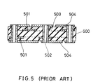
- FIG. 5 is a schematic view of this glass-epoxy multilayer substrate.
- reference numeral 500 denotes an insulating base material made of glass woven fabrics impregnated with epoxy resin; 501, Cu wirings in internal layers; 502, drilled holes made after being formed into a laminated multilayer; 503, a Cu layer on inner walls formed by a plating method; and 504, circuit patterns on the upper most layer.
- This drill process and the Cu-plated through-holes were established through the development of techniques in which this kind of glass-epoxy base material is used to connect internal layers to outside layers electrically. This method is also widely acknowledged in the world.
- SVH Semi-Buried Via Hole
- Via parts on the surface are filled with insulating resin which are then Cu-plated thereon in order to form mounting pads for components on top of the via parts.
- new multilayer substrates having a perfect inner-via-hole (IVH: Interstitional Via Hole) structure are disclosed, for example, in a SLC (Surface Laminated Circuit, registered trademark of IBM) substrate and a multilayer substrate using thermoplastic resin.
- a method of manufacturing SLC substrates comprises the steps of providing a double sided substrate having usual Cu-patterned layers, coating the surface of this substrate with resin as an insulating material, forming via holes by a photolithographic method, adding Cu-plating on the entire surface, and connecting a bottom conductor, a via hole part, and wiring on a surface layer. Then, by applying the same photolithographic method, patterns are formed. This process is repeated to form a multilayer.
- this method is especially watched with keen interest because it can form highly accurate wirings at an extremely low cost.
- the problems with this method is that the adhesion strength between the insulating material and the Cu-electrode is low, and substrates can warp easily due to the difference in thermal expansion between the core substrate and the resin.
- a multi layer substrate using thermoplastic resin is manufactured by first disposing holes in a thermoplastic sheet-type base material, and printing patterns on the surface of the sheet with conductive resin paste made of silver, and then, by heat-pressing another sheet formed separately on top to form a multilayer substrate.
- the problem in this case is that the thermoplastic resin does not have heat resistance.
- the conductive resin paste has high wiring resistance, and it is also difficult to solder the surface part. Nevertheless, both methods are attracting attention since they have the big advantage of forming multilayer substrates having a perfect inner-via-hole (IVH) structure.
- the above-mentioned conventional methods have the following problems.
- the conventional structure does not allow the processing of through-holes easily once the substrate is laminated into a multilayer substrate.
- This constitution presents difficulties for coping with the tendency toward high-density wiring. Namely, it is necessary to process even smaller holes, and it is also difficult to process holes to match the wirings in the internal layers.
- the diameter of the drill is required to be smaller and smaller, and the costs for processing this kind of drill become significant. It is also anticipated that accurate holes can not be formed in the thickness direction with minute drills.
- the conventional substrates used for circuits have a limit in the number of through-hole connections which can be performed per unit area and also in the density of circuit patterns. Therefore, the conventional method presents major difficulties for obtaining multilayer substrates used for high-density mounting which will be more and more in demand.
- EP-A-0 568 930 (which is a document under Article 54(3) EPC) relates to a method of manufacturing organic substrates used for printed circuits and to organic substrates manufactured thereby.
- the method includes the steps of forming through-holes in a porous raw material provided with free tackness films, filling electro-conductive paste into the through-holes, separating the free tackness films from the porous raw material filled with the electro-conductive paste in its through-holes, applying metal foils onto the surfaces of the porous raw material from which the free tackness films have been separated, and compressing the porous raw material applied with the metal foils through heating and pressurization, whereby the electro-conductive substances in the electro-conductive paste are connected for electrical connection between the metal foils.
- a further object of this invention is to provide a connecting member for the connection of circuit substrates which is suitable for an electrical connector of low electrical resistance.
- a connecting member for the connection of circuit substrates comprises an organic porous base material provided with tackfree films on both sides, wherein the connecting member has a plurality of through-holes at desired places, and the through-holes are filled with conductive resin compound up to the surface of the tackfree films.
- a method of manufacturing a multilayer circuit substrate comprises the steps of: providing a multilayer circuit substrate having at least two layers of circuit patterns, a circuit substrate having at least one layer of circuit pattern, and a connecting member of circuit substrates comprising an organic porous base material provided with tackfree films on both sides, wherein the connecting member has a plurality of through-holes, and the through-holes are filled with conductive resin compound up to the surface of the tackfree films from which the tackfree films are separated, positioning the connecting member of circuit substrates between the multilayer circuit substrate and the circuit substrate, and heating and pressurizing.
- Another method of manufacturing a multilayer circuit substrate comprises the steps of: providing a multilayer circuit substrate having at least two layers of circuit patterns and two pieces of a connecting member of circuit substrates comprising an organic porous base material provided with tackfree films on both sides, wherein the connecting member has a plurality of through-holes, and the through-holes are filled with conductive resin compound up to the surface of the tackfree films from which the tackfree films are separated, positioning the multilayer circuit substrate between the two connecting members of circuit substrates, applying a metal foil on both sides, heating and pressurizing and forming circuit patterns on the metal foils.
- the organic porous base material comprises a composite material comprised of nonwoven heat-resisting synthetic fiber fabrics impregnated with thermosetting resin.
- the nonwoven heat-resisting synthetic fiber fabrics comprise aramid resin, and that the thermosetting resin is epoxy resin.
- nonwoven heat-resisting synthetic fiber fabrics comprise paper, and that the thermosetting resin is one compound selected from the group consisting of phenol resin and epoxy resin.
- a conductive substance contained in the conductive resin compound is at least one metallic powder selected from the group consisting of silver, nickel, copper and an alloy thereof.
- a resin component contained in the conductive resin compound is the same as the thermosetting resin in the organic porous base material.
- the multilayer circuit substrate having at least two layers of circuit patterns and the circuit substrate having at least one layer of circuit pattern each comprise glass-epoxy multilayer circuit substrates having copper foil wirings and copper-plated through-holes.
- the multilayer circuit substrate having at least two layers of circuit patterns and the circuit substrate having at least one layer of circuit pattern each comprise aramid nonwoven fabrics and multilayer circuit substrates of thermosetting epoxy resin.
- the through-holes are formed by laser irradiation.
- the through-holes filled with the conductive resin compound have a diameter of 50 ⁇ m to 1 mm.
- the through-holes filled with the conductive resin compound have a pitch of 50 ⁇ m or more.
- the through-holes filled with the conductive resin compound have an electrical resistance of 0.05 to 5.0 m ⁇ .
- the porous base material has a porosity of from 2 to 35 %.
- the heating is carried out at a temperature of from 170 to 260 °C.
- the pressurization is carried out at a pressure of from 20 to 80 kg/cm 2 .
- a connecting member of circuit substrates comprises an organic porous base material provided with tackfree films on both sides, wherein the connecting member of circuit substrates has through-holes at requested places, and the through-holes are filled with conductive resin compound up to the surface of the tackfree films.
- This structure enables inner-via-hole connection, and thus, a connecting member of circuit substrates of high reliability and high quality can be attained. Furthermore, it is easy to determine fine pitchs at the conductive parts, and at the same time, this connecting member of circuit substrates is suitable for an electrical connector of low electrical resistance.
- this connecting member of circuit substrates is composed of a porous base material having compressibility resistance which comprises a composite material of nonwoven fabrics and thermosetting resin, and the porous base material has holes which are filled with conductive paste up to the surface of the tackfree films.
- the connecting member is possible to manufacture connecting members of circuit substrates stably and of high reliability with an ability to determine fine pitchs easily. Therefore, it is possible to form a high-layered substrate from a double sided substrate or a four-layer substrate without complications.
- the conductive resin compound is filled up to the surface of the tackfree films so that the conductive paste sticks out from the surface of the organic porous base material when the tackfree films are separated. If this connecting member is used for an electrical connector, these stick-out parts work favorably for electrical connection because electrical connection can take place easily through the stick-out parts.
- the connecting member of circuit substrates is held between a multilayer circuit substrate having at least two layers of circuit patterns and a circuit substrate having at least one layer of circuit pattern in which the tackfree films of the connecting member are already separated. And then, the whole assembly is provided with heat and pressure.
- the organic porous base material used has compressibility resistance and comprises a composite material of nonwoven fabrics and uncured thermosetting resin, and therefore, when the porous base material is compressed by heating and pressurization, the adhesion between the circuit substrates occurs strongly through the the thermosetting reaction within the above-mentioned connecting member of circuit substrates, and at the same time, the conductive paste is also compressed in this process.
- a binder component is pressed out between the conductive substances, thereby strengthening the binding between the conductive substances to each other and between the conductive substance and the metal foils.
- the conductive substance contained in the conductive paste becomes dense.
- the conductive paste is filled up to the surface of the tackfree films, the conductive paste sticks out from the surface of the organic porous base material when the tackfree films are separated. Accordingly, the filled amount of the conductive substance increases after the lamination, and thus, the connection resistance is reduced considerably.
- the binder component of the conductive paste filled into the through-holes penetrates into the porous base material side. This reduces the filled amount so that the conductive paste does not intrude between the porous base material and the metal foil applied on both sides any more, and accordingly, short-circuits can be prevented from occurring between the adjoining circuit patterns.
- a porous base material having compressibility resistance and comprising the composite material of the nonwoven fabrics and the thermosetting resin it is not only possible to connect the circuit substrates to each other, but the metal foils for the wirings on the upper most layers are also adhered strongly by heating and pressurization. It is also favorable to the environment that the plating processing is no longer necessary in the manufacturing process of multilayer circuit substrates.
- the multilayer circuit substrate is positioned between the two connecting members of circuit substrates from which the tackfree films are already separated. After a metal foil is applied on both sides, it is heated and pressurized, and then, the metal foils are formed into circuit patterns. In this way, multilayer circuit substrates are manufactured efficiently as in the case with the first manufacturing method.
- the organic porous base material comprises a composite material which is composed of nonwoven heat-resisting synthetic fiber fabrics impregnated with thermosetting resin.
- the multilayer circuit substrate is excellent in thermal and mechanical strength.
- the nonwoven heat-resisting synthetic fiber fabrics comprise aramid resin, while the thermosetting resin is epoxy resin.
- the multilayer circuit substrate is even more excellent in thermal and mechanical strength.
- the nonwoven heat-resisting synthetic fiber fabrics comprise paper, while the thermosetting resin is selected from the group consisting of phenol resin and epoxy resin. Accordingly, the multilayer circuit substrate is even more excellent in thermal and mechanical strength.
- the conductive substance contained in the conductive resin compound is at least one metallic powder selected from the group consisting of silver, nickel, copper and an alloy thereof.
- the multilayer circuit substrate is excellent in electrical conductivity.
- the resin component contained in the conductive resin compound is the same as the thermosetting resin in the organic porous base material.
- the conductive resin compound has excellent adhesion to the organic porous base material.
- the multilayer circuit substrate having at least two layers of circuit patterns and the circuit substrate having at least one layer of circuit pattern comprise glass-epoxy multilayer circuit substrates having copper foil wirings and copper-plated through-holes. As a result, it can be used in combination with conventional glass-epoxy multilayer circuit substrates.
- the multilayer circuit substrate having at least two layers of circuit patterns and the circuit substrate having at least one layer of circuit pattern comprise aramid nonwoven fabrics and multi layer circuit substrates of thermosetting epoxy resin, thereby forming multilayer substrates easily.
- the through-holes are formed by laser irradiation. This method is more suitable for forming fine-pitched holes than by a drill. In addition, there is no dust created in this process.
- the through-holes filled with the conductive resin compound have a diameter of 50 ⁇ m to 1 mm, thereby forming the conductive part with a desirable diameter.
- An even more preferable diameter is from 100 to 300 ⁇ m.
- the through-holes filled with the conductive resin compound have a pitch (a distance between the filled parts) of 50 ⁇ m or more. As a result, the filled parts are completely insulated from each other.
- the through-holes filled with the conductive resin compound have an electrical resistance of 0.05 to 5.0 m ⁇ . This resistance provides good continuity for practical use as a circuit substrate or as a connector. A more preferable range is 0.1 to 0.8 m ⁇ .
- the porous base material has a porosity of from 2 to 35 %. This is practical since an “anchor" effect with the conductive paste can be attained.
- the heating is carried out at a temperature of from 170 to 260 °C.
- a thermosetting resin is used, a hardening reaction can be effectively conducted.
- the pressurization is carried out at a pressure of from 20 to 80 kg/cm 2 .
- the substrate has effective properties by substantially diminishing air holes inside the substrate.
- the electric connecting member comprising the porous base material having compressibility resistance and consisting of a composite material of heat-resisting organic reinforcement and uncured thermosetting resin in which the holes are filled with the conductive paste up to the surface of the tackfree films, it is possible to connect double sided substrates or four-layer substrates to each other electrically and mechanically without any problems, particularly in manufacturing. Therefore, double sided substrates can be easily formed into multilayer substrates having an inner via structure.
- the porous base material having compressibility resistance a composite material can be used which is composed of organic reinforcement and uncured thermosetting resin. Therefore, when the porous base material is compressed by heating and pressurization, the conductive paste is also compressed in this process.
- the organic binder component pressed out between the conductive substances, hardens and strengthens the binding between the conductive substances and between the conductive substance and the metal foil. Accordingly, the conductive substance within the conductive paste becomes dense. This leads to via connection of extremely low resistance.
- the conductive paste is filled up to the surface of the tackfree films, the conductive paste sticks out from the surface of the organic porous base material when the tackfree films are separated. As a result, the filled amount of the conductive substance increases after the lamination, and thus, the connection resistance is reduced considerably.
- the binder component of the conductive paste filled into the through-holes penetrates into the porous base material side. This reduces the filled amount so that the conductive paste does not intrude between the porous base material and the metal foil applied on both sides. As a result, short-circuits can be prevented from occurring between adjoining circuit patterns.
- a thermosetting resin of the porous base material having compressibility resistance and comprising the composite material of an organic reinforcement and thermosetting resin it is not only possible to connect the circuit substrates to each other, but the wirings of metal foils can be connected electrically by heating and pressurization.
- the connecting member for the connection of circuit substrates of this invention is suitable for connecting circuit substrates to each other.
- This connecting member is also effective for connecting circuit substrates to devices electrically and mechanically.
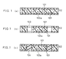
- FIG. 1 (a) - (c) are cross-sectional views showing a method of manufacturing a connecting member for the connection of circuit substrates of a first embodiment to a fourth embodiment of this invention.
- FIG. 1 (a) shows a step in which tackfree films are disposed on both sides of an organic porous base material.
- FIG. 1 (b) shows a step in which through-holes are formed.
- FIG. 1 (c) shows a step in which conductive paste is filled into the through-holes.
- FIG. 2 is a cross-sectional view of a multilayer circuit substrate using a connecting member for circuit substrates of a substrate using a connecting member for circuit substrates of a fifth embodiment to a eighth embodiment of this invention.
- FIG. 3 is a cross-sectional view of a multilayer circuit substrate using a connecting member for circuit substrates of a ninth embodiment to a twelfth embodiment of this invention.
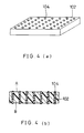
- FIG. 4 (a) is a perspective view and FIG. 4 (b) is a cross-sectional view of an electrical connector using a connecting member for circuit substrates in a thirteenth embodiment of this invention.
- FIG. 5 is a cross-sectional view showing a glass-epoxy multilayer substrate manufactured in a conventional method.
- a connecting member for the connection of circuit substrates and a method of manufacturing a multilayer circuit substrate by using the connecting member will be explained in one embodiment of this invention.
- the conductive paste of this embodiment is composed of a metallic filler, thermosetting resin, and a hardener.
- the conductive filler According to the main object of this conductive filler, it should be contained in the conductive compound in high concentration. The reason for this is that, as mentioned above, conductive reliability must be maintained by raising the contact probability of the conductive fillers to each other even if the substrates are distorted due to lower resistance of connected via holes or due to thermal and mechanical stress. Silver, copper or nickel are illustrative examples of conductive fillers, and it is also possible to use two different kinds or more of these metals simultaneously. As long as the conductive filler has the characteristics mentioned above, it can be a spherical shape or of a flaked form etc.
- the adhesion process by heating and pressurization is preferably conducted in an atmosphere in which the oxygen content is 1.0 % or less.
- the connecting member for the connection of circuit substrates of this invention is formed by heating and pressurization in a closed state in order to connect the metal foils electrically. Therefore, it is inconvenient to include a volatile constituent such as solvent because it can lead to causing internal blisters.
- a liquid resin as the epoxy resin.
- suitable epoxy resins are liquid-type epoxy resins including two or more epoxy radicals, for example, bisphenol A-type epoxy resin, bisphenol F-type epoxy resin, alicyclic epoxy resin, and amine epoxy resin etc.
- any ordinary hardener can be used.
- Generally used hardeners include amine hardeners, e.g. dicyandiamide and carboxylic acid hydrazide, urea hardeners, e.g. 3-(3,4-dichlorophenyl)-1,1-dimethyl urea, acid anhydride hardeners, e.g. phthalic anhydride, pyromellitic acid anhydride, and hexahydro phthalic acid anhydride, and aromatic amine hardeners, e.g. diamide diphenylmethane, diamide diphenylsulfonic acid (amine adduct). It is preferable to use solid-type subclinical hardener powder, particularly in view of stability and workability.
- Tackfree films in the connecting member for the connection of circuit substrates function as pollution control films during the processes of forming holes and filling the conductive paste, but also during transportation.
- the films are separated when circuit substrates are connected, and therefore, they must have enough adhesion strength until they are used, while they are to be separated easily in use.
- the tackfree films are preferably to be adhered in a heated environment at a temperature at which the thermosetting resin of the porous base material does not begin to cure.
- the films are preferably of non-heat-contraction-type.
- PET sheet polyethylene terephthalate
- PP polyethylene terephthalate
- the base material used in the connecting member for the connection of circuit substrates of this embodiment is at least an organic porous base material.
- a well-known laminated base material can be used.
- a laminated base material used for circuit substrates is a composite material of inorganic or organic reinforcement and thermosetting resin. The reinforcement has the functions of strengthening the circuit substrate itself and controlling the warp caused by the heat when parts are mounted on the substrate.
- inorganic reinforcement examples are glass woven fabrics containing woven glass fibers and nonwoven fabrics consisting of glass fibers cut to a length of several mm to several 10 mm.
- the glass cloth is made by weaving filaments of 5 to 15 ⁇ m in diameter as warps and twines (yarn) bonding several hundreds pieces as wefts together.
- the glass which is generally used for printed substrates is composed mainly of SiO 2 , CaO, Al 2 O 3 , and B 2 O 3 which are called E-glass.
- the glass nonwoven fabrics are mainly glass nonwoven paper which is produced by cutting the above-noted glass fibers into paper and adhering them together with water dispersible epoxy resin. Occasionally, an inorganic filler is added for the purpose of improving the dimensional stability.
- organic reinforcement examples are woven or nonwoven fabrics (e.g. commodity name "THERMOUNT” manufactured by E.I.Dupont) made of paper or aromatic polyamide fibers (e.g. commodity name "KEVLAR” manufactured by E.I.Dupont).
- THERMOUNT Trademark
- THERMOUNT is produced by first cutting the above-noted KEVLAR fabrics of para-type aramid at a length of about 6.7 mm, adding about 10 to 15 % by weight of filmed meta-type aramid to form paper, and calendering under high temperature and high pressure after being dried (e.g. U.S. Patent No. 4,729,921).
- Substrates using aramid are attracting attention for their use in MCM because of the excellent heat resistance and small coefficient of thermal expansion (e.g. IEEE TRANSACTIONS OF COMPONENTS, HYBRIDS, AND MANUFACTURING TECHNOLOGY, VOL.13, NO. 3, SEPTEMBER 1990, PP.570-PP.575).
- a prepreg is a composite material consisting of reinforcement and uncured resin in which the above-described reinforcement is impregnated with thermosetting resin from which the solvent is removed.
- it is in the form of a glass epoxy prepreg or an aramid epoxy prepreg in which the former prepreg consists of glass woven fabrics and epoxy resin and the latter consists of aramid reinforcement and epoxy resin.
- prepreg is used for expressing the step up to the point where resin cures through heating and pressurization when double sided substrates and multilayer substrates are manufactured.
- Thermosetting resin is an insoluble and infusible macromolecule having a three-dimensional knitting structure of molecules which melt, undergo propagation reaction and crosslinking reaction by heat.
- a thermosetting resin for printed substrates is selected in view of heat resistance and solvent resistance. Examples include epoxy, phenol, melamine, and polyester. By adding a sub-material, such as a hardener, a modifier or a filler, thermosetting resins of various reaction temperatures can be obtained.
- Epoxy resin is most widely used among different kinds of thermosetting resins and is characterized by excellent mechanical, electrical, and chemical properties. Recently, ordinary epoxy resin is modified in various ways to meet the needs toward higher mounting density and higher heat resistance.
- novolak epoxy resin in which novolak-type phenol is used for the purpose of enhancing heat resistance.
- a flame retarder is added to attain not only heat resistance, but also flame resistance.
- a conductor used for metal foil in this example is copper in the form of foil. Thicknesses of 18 to 70 microns are used widely as the copper foils, and they are usually electrolytic copper foils. Copper foil suitable for use in the connecting member of circuit substrates in this invention is placed such that the treated copper foil side is generally used for the electrical connecting surface in view of via connection through the conductive paste. The reason for this is that the treated degree is important with respect to reliability of connection. In other words, the rougher the surface is treated, the better results can be attained in the connection resistance, electrical strength and reliability.
- a copper foil which is treated by oxidizing treatment can not be used for electrical connecting parts for circuit substrates to be connected. This is due to the fact that the oxide treated side forms an oxide copper layer which is insulated electrically. Therefore, no connection can be achieved. It is preferable that the surface part of copper foil on the substrates to be connected is treated copper foil as mentioned above.
- the evaluation method of via connection resistance in a circuit substrate manufactured by the connecting member for circuit substrates of this invention is to measure two different resistances, namely, to measure connection resistance per each via and to measure connection resistance when 500 via connections are chained in line for wirings.
- connection resistance per each via is measured by a four-terminal resistance measurement conducted at both ends of metal wirings of both via ends.
- the serial resistance of 500 pieces can be evaluated in a method which is mainly used for reliability tests. This method is conducted by first adding the resistance for 500 pieces and the resistance of metallic wirings by the above-noted four-terminal measurement method, and then, subtracting the initial resistance amount from the measured amount after the experiment. In other words, this method determines the amount of change in via resistance of 500 pieces.
- a heat cycle test is based on the amount of change in via connection resistance after 30 minutes at -55°C in vapor phase, and then, after 30 minutes at +125°C a thousand times.
- the evaluation standard is that the amount of change in via serial substrate of 500 pieces is 250 m ⁇ or less. This is equivalent to a change in 0.5 m ⁇ or less per each via.
- a solder dipping test is conducted by first dipping for 10 seconds in a solder vessel heated and dissolved at 230°C, and then measuring the amount of change in via connection resistance in the same manner as mentioned above.
- the evaluation standard is the same as above.
- An oil-dipping test is a heat cycle test conducted in the oil part of a liquid phase.
- a sample substrate is dipped 10 seconds in the oil which is heated up to 260°C, maintained 10 seconds at room temperature, and further dipped 10 seconds in the oil at 20°C.
- the evaluation takes place after this heat cycle is repeated 200 times. At this time, it is measured whether the resistance shows no breakage during 200 times when it is dipped in the higher and lower temperature sides. At the same time, the amount of change in resistance is measured and evaluated according to the same evaluation standard mentioned above.
- a connecting member for the connection of circuit substrates and a method of manufacturing a multilayer circuit substrate by using the connecting member will be explained by referring to the attached figures in one embodiment of this invention.
- prepregs used for the connecting member for the connection of circuit substrates are shown in Prepreg 1 to 4.
- thermosetting resin epoxy resin with high glass transition point was used which was in this case Shell EPON 1151B60 of 180°C in the glass transition point.
- MEK methylethylketone
- Glass nonwoven fabrics were also used as inorganic reinforcement, and the impregnated resin was the same with in Prepreg 1.
- the glass unwoven fabrics used were made into glass nonwoven paper by cutting the above-mentioned glass fabrics to paper and by adhering them together with water dispersible epoxy resin.
- An inorganic filler of alumina powder was added to improve the dimensional stability.
- the amount of impregnated resin was about 40 wt% against the glass woven fabrics, and the thickness of the prepreg was 140 ⁇ m.
- Nonwoven fabric paper of aromatic polyamid was used as an organic reinforcement which was in this case "THERMOUNT" manufactured by E.I. Dupont of 72 g/m 2 in basis weight and 0.5 g/cc in paper density.
- the impregnated resin was epoxy resin of Dow DER 532A80, and the glass transition point was 140°C.
- the resin impregnation and the drying process took place in the same method as in Prepreg 1.
- the amount of impregnated resin was 52 wt%, and the thickness of the prepreg was 150 ⁇ m.
- Paper as an organic reinforcement was also used here which was in this case paper phenol prepreg.
- the paper used was kraft paper of 70 g/m 2 in basis weight.
- Thermosetting resin was modified resin added with alkyl phenol group.
- the amount of resin was 48 wt% against the kraft paper, and the thickness of the prepreg was 145 ⁇ m.
- Composition of the conductive paste of this invention is shown in TABLE 1.
- Metallic fillers of silver, copper and nickel were used in a spherical and flake form.
- the resin compound was bisphenol A-type epoxy resin (EPICOAT 828 manufactured by Yuka Shell Epoxy Co., Ltd.), and the harder used was Amineadduct (MY-24 manufactured by Ajinomoto Co., Ltd.).
- TABLE 1 shows the form of the metal particle, the average size of the particle, the mixed amount (% by weight), and the viscosity of the paste of 0.5 rpm in an E-type viscometer at room temperature.
- Metal Resin Compound Metal Form Particle size ( ⁇ m) Amount of metal (wt%) Amount of resin (wt%) Amount of hardener (wt%) Viscosity (Pa ⁇ s) P-1 Cu spherical 2 85 12 3 120 P-2 Cu spherical 2 87.5 10 2.5 340 P-3 Ni spherical 1.2 85 12 3 300 P-4 Ni spherical 1.2 87.5 10 2.5 550 P-5 Ag flake 1.8 85 12 3 220 P-6 Ag flake 1.8 87.5 10 2.5 475
- FIGS. 1 (a) to (c) are cross-sectional views showing a method of manufacturing a connecting member for the connection of circuit substrates in the embodiment of this invention by using the above-mentioned Prepregs 1 to 4.
- a porous base material 102 (Prepreg 3) was prepared which was provided with tackfree films 101 (thickness of about 12 ⁇ m) made of polyester on both sides.
- the method of applying the tackfree films is to position the above prepreg between the tackfree films, and to position it further between stainless steel plates. After that, it is heated four minutes at a temperature of 110°C and pressurized with 20 Kg/cm 2 . At this moment, the prepreg is compressed by the heating and pressurization so that internal pores 102a decrease.
- an aramid-epoxy sheet having tackfree films is obtained.
- through-holes 103 (diameter of about 250 ⁇ m) were formed into aramid-epoxy sheet 102 (thickness of about 130 ⁇ m) at predetermined places by a carbon dioxide laser, as shown in FIG. 1 (b).
- conductive paste 104 is filled into through-holes 103 to form the connecting member for circuit substrates of this invention.
- conductive paste 104 As shown in the filling method of conductive paste 104, aramid-epoxy sheet 102 having through-holes 103 was placed on a table of a printing machine (not shown), and conductive paste 104 was printed directly from above on tackfree films 101.
- Tackfree film 101 on the upper surface serves as a printing mask and also prevents the surface of aramid-epoxy sheet 102 from soiling.
- Circuit substrates to be combined were two pairs of double sided board comprising glass-epoxy substrate.
- This glass-epoxy double sided boards were produced from glass woven fabrics laminated with four sheets of prepreg (thickness of about 100 ⁇ m) which is impregnated with thermosetting resin equivalent to FR-4, as in the above-mentioned case. Then, a copper foil which was treated on both sides was laminated with a thickness of 35 ⁇ m on both sides of the substrates.
- the substrates were cured and adhered to the copper foils.
- the substrates manufactured in this manner were disposed with holes of 0.6 mm in diameter at predetermined places by using a drill machine.
- FIG. 2 shows a cross-sectional view of this embodiment before being laminated.
- reference numeral 305 is a glass-epoxy substrate; 307, drilled holes; 308, a copper-plated inner wall; and 306, circuit patterns of copper. Connecting member for circuit substrates 309 is placed between the above-mentioned double sided boards.
- the above-noted double sided boards have a connecting land at places to be connected electrically, and the land part is positioned to meet conductive paste 304 of the connecting member for circuit substrates mentioned above. It is therefore necessary to be arranged in such a way that the drilled through-hole parts do not come in contact with the conductive paste part of the above-mentioned connecting member for circuit substrates.
- the multilayer member manufactured in this manner is a four-layer substrate having four layers of circuit patterns in which the epoxy resin of the above-mentioned connecting member for circuit substrates flowed into the through-hole parts of the above-noted double sided board, thereby forming a complete closed structure. This four-layer substrate was tested and the results of different reliability tests are shown in TABLE 3.
- the aramid-epoxy double sided substrate manufactured by the connecting member for circuit substrates was also used instead of the glass-epoxy double sided circuit substrate held between the above-mentioned connecting members for circuit substrates with the same satisfactory properties being achieved
- the connecting member for circuit substrates will be explained in this embodiment of the invention.
- the same connecting member for circuit substrates was used as in Examples 1 to 4.
- FIG. 3 is a cross-sectional view of a multilayer circuit substrate before being laminated in one embodiment of this invention, and the description follows by referring to the figure.
- a circuit substrate to be combined was a four-layer substrate consisting of a glass-epoxy substrate.
- This four-layer substrate was manufactured from glass woven fabrics laminated with four sheets of the prepreg (thickness of about 100 ⁇ m) impregnated with thermosetting resin as in the case mentioned above. Then, a copper foil which was treated on one side was applied with a thickness of 35 ⁇ m on both sides of the substrates. By heating and pressurizing about one hour at the temperature of 170°C and 40 Kg/cm 2 in vacuum by heat-pressing, the substrate was cured and adhered to the copper foils.
- a photolithography method was used to form circuit patterns.
- dry films were applied on both sides by using a laminater, and then patterns were exposed. After that, the processes of development, etching and separation of the dry films followed.
- the copper foil surface of the substrate with the above patterns was treated, and further, two sheets of the above-noted prepreg were disposed on both sides.
- the treated surface of the one-side treated copper foil was placed on both sides such that the treated surfaces face inside, and they were laminated once more by heat-pressing.
- This substrate was disposed with holes of 0.6 mm in diameter at requested places by using a drill machine.
- circuit patterns were formed on the upper layer by means of a photolithography method.
- the four-layer glass epoxy substrate manufactured in this manner was placed as an intermediate layer between the connecting members for circuit substrates from which the tackfree films had been separated on both sides. As shown in FIG. 3, they were positioned for the lamination together with the one-side treated copper foils and were subjected to heating and pressurization by heat-pressing under the same conditions as mentioned above.
- the copper foils on the surface of this multilayer substrate were formed into patterns by the same photolithographic method. Referring to FIG.
- reference numeral 410 denoted the above-mentioned four-layer glass-epoxy substrate; 411, drilled holes; 412, a copper-plated inner wall; and 413, circuit patterns of copper formed by the photolithographic method.
- the above-noted four-layer glass-epoxy substrate was held between connecting members for circuit substrates 414 and 415, which are again held between one-side treated copper foils 416 and 417.
- the above-noted four-layer substrate and the connecting members for circuit substrates have connecting land 419 at places to be connected electrically and conductive paste part 418.
- the above-mentioned land part was positioned to meet conductive paste 418 of the connecting members for circuit substrates mentioned above. It is therefore necessary to position in such a way that the drilled through-hole parts do not come in contact with the conductive paste part of the above-mentioned connecting members for circuit substrates.
- a multilayer member manufactured in this manner is a six-layer substrate having six layers of wirings in which the above-mentioned connecting members for circuit substrates are filled with the epoxy resin flowed into the through-hole parts of the above-noted double sided board, thereby forming a complete closed structure.
- Another method of obtaining a substrate with multilayer circuit patterns is to prepare a desirable number of the above-mentioned intermediate multilayer members and the connecting members for circuit substrates and to laminating them at once.
- the aramid-epoxy double sided substrate manufactured by the above-noted connecting member for circuit substrates was used instead of the four-layer glass-epoxy circuit substrate held between the connecting members for circuit substrates with the same satisfactory properties being shown.
- circuit substrates and the connecting members for circuit substrates used had been already checked so that a high processing yield could be preserved at a controlled cost increase.
- the first circuit substrate and the second circuit substrate are connected to each other through the compressibility of the connecting members of circuit substrates by heating and pressurization. As a result, a highly laminated substrate can be manufactured rather easily.
- the porous base material of about 150 to 170 ⁇ m in thickness which was used in the first embodiment was applied on both sides with fluorocarbon tackfree films (tetrafluoroethylene-ethylene copolymer manufactured by Asahi Garasu Co., Ltd., commodity name: Aflex) of about 30 ⁇ m in thickness.
- fluorocarbon tackfree films tetrafluoroethylene-ethylene copolymer manufactured by Asahi Garasu Co., Ltd., commodity name: Aflex
- an excimer laser was used to form through-holes of about 200 ⁇ m in diameter.
- the distance (pitch) between the holes was set at about 200 ⁇ m.
- conductive paste was filled into the through-holes.
- an aramid-epoxy sheet having through-holes was placed on a table of a printing machine (not shown), and the conductive paste 104 was printed directly from above on tackfree films 1. At this moment, the tackfree film on the upper surface serves as a printing mask and also prevents the surface of the aramid-epoxy sheet from soiling.
- the conductive paste used was silver powder with an average diameter of 2 ⁇ m as conductive filler, and the resin was the same thermosetting epoxy resin (non-solvent type) as in the above-noted substrate material.
- a hardener was obtained by kneading and mixing three rolls of acid anhydride-type hardener each having 85, 12.5, and 2.5% by weight sufficiently.
- FIGS. 4 (a) and (b) are examples of electrical connectors obtained in the manner mentioned above.
- FIG. 4 (a) is a perspective view of an electrical connector
- FIG. 4 (b) is a cross-sectional view of the same.
- reference numeral 102 denotes an organic porous base material (aramid epoxy sheet); and 104, conductive resin compound part. This electrical connector can conduct electricity only in the vertical direction, not in the horizontal direction.
- conductive resin compound 104 is formed with a pitch of three roles per 1 mm. Conductive resin compound 104 sticks out about 30 ⁇ m which makes it suitable for connecting NESA glass of liquid-crystal elements and a flexible printed substrate (FPC). Additionally, when an adhesive is applied on surface A and surface B, it can easily stick to other circuit substrates.
- the connecting for circuit substrates of the above-The connecting member for circuit substrates of the above-mentioned embodiment can be used, for example, as an electrical connector for connecting NESA glass of liquid-crystal elements and a flexible printed substrate (FPC) or as an electrical connector for connecting a driver circuit of electrical signal conductor in a movable telephone and a FPC.
- FPC flexible printed substrate
- the connecting member for the connection of circuit substrates comprising the porous base material having compressibility resistance and consisting of a composite material of nonwoven fabrics and thermosetting resin which is also provided with tackfree films and holes filled with the conductive paste up to the surface of the tackfree films, it is possible to form a high-layered substrate easily from double sided boards or four-layer substrates which can be manufactured rather stably.
- the connecting member for circuit substrates of the embodiments is used, the porous base material is compressed by heating and pressurization so that the conductive paste is also compressed.
- a binder component which is pressed out between the conductive substances strengthens the binding between the conductive substances to each other and between the conductive substance and the metal foil, and accordingly, the conductive substance contained in the conductive paste becomes dense.
- the conductive paste since the conductive paste is filled up to the surface of the tackfree films, the conductive paste sticks out from the surface of the organic porous base material when the tackfree films are separated. As a result, the filled amount of the conductive substance increases after the lamination, and thus, the connection resistance is reduced considerably.
- porous base material having compressibility resistance and comprising a composite material of nonwoven fabrics and thermosetting resin it is not only possible to connect the circuit substrates to each other, but the metal foil for wirings on the upper most layer can be also adhered strongly by heating and pressurization. It is also favorable to the environment that a drilling process or a plating process is not necessary any more in the manufacturing process of multilayer circuit substrates.
- the connecting member for the connection of circuit substrates comprises an organic porous base material provided with tackfree films on both sides, wherein the connecting member for circuit substrates has through-holes at requested places, and the through-holes are filled with conductive resin compound up to the surface of the tackfree films.
- This structure enables inner-via-hole connection and can therefore attain the connecting member for circuit substrates of high reliability and high quality. Additionally, it is easy to determine fine pitchs at the conductive parts, and an electrical connector of low electrical resistance can be attained.
Landscapes
- Engineering & Computer Science (AREA)
- Manufacturing & Machinery (AREA)
- Microelectronics & Electronic Packaging (AREA)
- Production Of Multi-Layered Print Wiring Board (AREA)
- Printing Elements For Providing Electric Connections Between Printed Circuits (AREA)
Claims (18)
- Elektrisches Verbindungsteil zur Verbindung von Schaltungssubstraten, wobei das elektrische Verbindungsteil ein organisches poröses Grundmaterial (102), das auf beiden Seiten mit nicht klebrigen Folien (101) versehen ist, und Durchgangslöcher (103) durch das organische poröse Grundmaterial (102) aufweist, die mit einer leitfähigen Harzverbindung (104) gefüllt sind, wobei die leitfähige Harzverbindung bis zur Oberfläche der nicht klebrigen Folien eingefüllt ist und die Dicke der nicht klebrigen Folien derartig ist, daß die leitfähige Harzverbindung nach Abtrennung der nicht klebrigen Folien auf beiden Seiten von der Außenfläche des organischen porösen Grundmaterials (102) vorsteht, um die elektrische Verbindung zwischen den Schaltungssubstraten zu verbessern.
- Verfahren zur Herstellung eines elektrischen Verbindungsteils zur Verbindung von Schaltungssubstraten, wobei das Verfahren die Schritte aufweist:(a) Bereitstellen eines organischen porösen Grundmaterials (102) mit nicht klebrigen Folien (101) auf beiden Seiten, wobei das organische poröse Grundmaterial (102) Durchgangslöcher (103) hat und die Durchgangslöcher bis an die Oberfläche der nicht klebrigen Folien mit einer leitfähigen Harzverbindung (104) gefüllt sind,(b) Abtrennen der nicht klebrigen Folien von dem Verbindungsteil, so daß die leitfähige Harzverbindung (104) von der Oberfläche des organischen porösen Grundmaterials (102) vorsteht.
- Verfahren zur Herstellung eines Mehrschicht-Schaltungssubstrats mit den Schritten:(a) Bereitstellen eines Mehrschicht-Schaltungssubstrats (305) mit mindestens zwei Schichten von Schaltungsstrukturen (306), einem Schaltungssubstrat (305) mit mindestens einer Schaltungsstrukturschicht (306) und einem elektrischen Verbindungsteil (309) für die Substrate (305), wobei das elektrische Verbindungsteil (309) ein organisches poröses Grundmaterial (302) und Durchgangslöcher durch das organische poröse Grundmaterial (102) aufweist, wobei die Durchgangslöcher mit einer leitfähigen Harzverbindung (304) gefüllt sind, die auf beiden Seiten von der Außenfläche des organischen porösen Grundmaterials (302) vorsteht,(b) Positionieren des Verbindungsteils (309) zwischen dem Mehrschicht-Schaltungssubstrat (305) und dem Schaltungssubstrat (305) und(c) Erwärmen und Druckbeaufschlagung.
- Verfahren zur Herstellung eines Mehrschicht-Schaltungssubstrats mit den Schritten:(a) Bereitstellen eines Mehrschicht-Schaltungssubstrats (410) mit mindestens zwei Schichten von Schaltungsstrukturen (413) und zwei elektrischen Verbindungsteilen (414, 415) wobei jedes der elektrischen Verbindungsteile (414, 415) ein organisches poröses Grundmaterial und Durchgangslöcher durch das organische poröse Grundmaterial aufweist, wobei die Durchgangslöcher mit einer leitfähigen Harzverbindung (418) gefüllt sind, die auf beiden Seiten von der Außenfläche des organischen porösen Grundmaterials vorsteht,(b) Positionieren des Mehrschicht-Schaltungssubstrats (410) zwischen zwei elektrischen Verbindungsteilen (414, 415);(c) Aufbringen einer Metallfolie auf beiden Seiten; und(d) Erwärmen und Druckbeaufschlagung und Ausbilden von Schaltungsstrukturen auf den Metallfolien.
- Elektrisches Verbindungsteil und Verfahren nach einem der Ansprüche 1 bis 4, wobei das organische poröse Grundmaterial ein Verbundmaterial ist, das einen wärmebeständigen synthetischen Faservliesstoff aufweist, der mit einem ungehärteten wärmehärtbaren Harz imprägniert ist.
- Elektrisches Verbindungsteil und Verfahren nach Anspruch 5, wobei der wärmebeständige synthetische Faservliesstoff Aramidharz aufweist und das ungehärtete wärmehärtbare Harz Epoxidharz ist.
- Elektrisches Verbindungsteil und Verfahren nach Anspruch 5, wobei der wärmebeständige synthetische Faservliesstoff Papier aufweist und das ungehärtete wärmehärtbare Harz aus der Gruppe gewählt ist, die aus Phenolharz und Epoxidharz besteht.
- Elektrisches Verbindungsteil und Verfahren nach einem der Ansprüche 1 bis 7, wobei eine leitfähige Substanz, die in der leitfähigen Harzverbindung enthalten ist, mindestens ein Metallpulver ist, das aus der Gruppe gewählt ist, die aus Silber, Nickel, Kupfer, Silberlegierung, Nickellegierung und Kupferlegierung besteht.
- Elektrisches Verbindungsteil und Verfahren nach einem der Ansprüche 1 bis 8, wobei eine Harzkomponente, die in der leitfähigen Harzverbindung enthalten ist, die gleiche ist wie das wärmehärtbare Harz in dem organischen porösen Grundmaterial.
- Verfahren zur Herstellung eines Mehrschicht-Schaltungssubstrats nach Anspruch 3 oder 4, wobei das Mehrschicht-Schaltungssubstrat mit zumindest zwei Schichten von Schaltkreisstrukturen und/oder das Schaltungssubstrat mit zumindest einer Schaltungsstrukturschicht Glas-Epoxidharz-Substrate mit Kupferfolienverdrahtungen und verkupferten Durchgangslöchern aufweisen.
- Verfahren zur Herstellung eines Mehrschicht-Schaltungssubstrats nach Anspruch 3 oder 4, wobei das Mehrschicht-Schaltungssubstrat mit zumindest zwei Schichten von Schaltungsstrukturen und/oder das Schaltungssubstrat mit zumindest einer Schaltungsstrukturschicht Aramidvliesstoffe und wärmehärtbares Epoxidharz ausweisen.
- Elektrisches Verbindungsteil und Verfahren nach einem der Ansprüche 1 bis 11, wobei die Durchgangslöcher durch Laserstrahlung ausgebildet werden.
- Elektrisches Verbindungsteil und Verfahren nach einem der Ansprüche 1 bis 12, wobei die Durchgangslöcher, die mit der leitfähigen Harzverbindung gefüllt sind, einen Durchmesser von 50 µm bis 1 mm haben.
- Elektrisches Verbindungsteil und Verfahren nach einem der Ansprüche 1 bis 13, wobei die Durchgangslöcher, die mit der leitfähigen Harzverbindung gefüllt sind, einen Abstand von 50 µm oder mehr haben.
- Elektrisches Verbindungsteil und Verfahren nach einem der Ansprüche 1 bis 14, wobei die Durchgangslöcher, die mit der leitfähigen Harzverbindung gefüllt sind, einen elektrischen Widerstand von 0,05 bis 5,0 mΩ haben.
- Elektrisches Verbindungsteil und Verfahren nach einem der Ansprüche 1 bis 15, wobei das poröse Grundmaterial eine Porosität von 2 bis 35 % hat.
- Verfahren zur Herstellung eines Mehrschicht-Schaltungssubstrats nach Anspruch 3 oder 4, wobei die Erwärmung mit einer Temperatur von 170 bis 260 °C erfolgt.
- Verfahren zur Herstellung eines Mehrschicht-Schaltungssubstrats nach Anspruch 3 oder 4, wobei die Druckbeaufschlagung mit einem Druck von 20 bis 80 kg/cm2 erfolgt.
Applications Claiming Priority (4)
| Application Number | Priority Date | Filing Date | Title |
|---|---|---|---|
| JP234519/93 | 1993-09-21 | ||
| JP23451993 | 1993-09-21 | ||
| JP242450/93 | 1993-09-29 | ||
| JP24245093 | 1993-09-29 |
Publications (2)
| Publication Number | Publication Date |
|---|---|
| EP0645950A1 EP0645950A1 (de) | 1995-03-29 |
| EP0645950B1 true EP0645950B1 (de) | 1998-09-02 |
Family
ID=26531606
Family Applications (1)
| Application Number | Title | Priority Date | Filing Date |
|---|---|---|---|
| EP19940114796 Expired - Lifetime EP0645950B1 (de) | 1993-09-21 | 1994-09-20 | Verbindungsteil eines Schaltungssubstrats und Verfahren zur Herstellung mehrschichtiger Schaltungssubstrate unter Verwendung dieses Teils |
Country Status (4)
| Country | Link |
|---|---|
| US (3) | US5484647A (de) |
| EP (1) | EP0645950B1 (de) |
| CN (1) | CN1075338C (de) |
| DE (1) | DE69412952T2 (de) |
Cited By (2)
| Publication number | Priority date | Publication date | Assignee | Title |
|---|---|---|---|---|
| DE102004045451A1 (de) * | 2004-09-20 | 2006-03-30 | Atotech Deutschland Gmbh | Galvanisches Verfahren zum Füllen von Durchgangslöchern mit Metallen, insbesondere von Leiterplatten mit Kupfer |
| US8784634B2 (en) | 2006-03-30 | 2014-07-22 | Atotech Deutschland Gmbh | Electrolytic method for filling holes and cavities with metals |
Families Citing this family (162)
| Publication number | Priority date | Publication date | Assignee | Title |
|---|---|---|---|---|
| JP2756075B2 (ja) * | 1993-08-06 | 1998-05-25 | 三菱電機株式会社 | 金属ベース基板およびそれを用いた電子機器 |
| JPH08148240A (ja) * | 1994-09-20 | 1996-06-07 | Whitaker Corp:The | コネクタ |
| FR2726397B1 (fr) * | 1994-10-28 | 1996-11-22 | Commissariat Energie Atomique | Film conducteur anisotrope pour la microconnectique |
| JP3311899B2 (ja) * | 1995-01-20 | 2002-08-05 | 松下電器産業株式会社 | 回路基板及びその製造方法 |
| US5837356A (en) * | 1995-09-22 | 1998-11-17 | Kyocera Corporation | Wiring board and method for manufacturing the same |
| EP0774888B1 (de) | 1995-11-16 | 2003-03-19 | Matsushita Electric Industrial Co., Ltd | Gedruckte Leiterplatte und ihre Anordnung |
| JP3241605B2 (ja) | 1996-09-06 | 2001-12-25 | 松下電器産業株式会社 | 配線基板の製造方法並びに配線基板 |
| US6703565B1 (en) * | 1996-09-06 | 2004-03-09 | Matsushita Electric Industrial Co., Ltd. | Printed wiring board |
| JP3889856B2 (ja) * | 1997-06-30 | 2007-03-07 | 松下電器産業株式会社 | 突起電極付きプリント配線基板の製造方法 |
| TW410534B (en) * | 1997-07-16 | 2000-11-01 | Matsushita Electric Industrial Co Ltd | Wiring board and production process for the same |
| US5902438A (en) * | 1997-08-13 | 1999-05-11 | Fry's Metals, Inc. | Process for the formation of anisotropic conducting material |
| US6376049B1 (en) * | 1997-10-14 | 2002-04-23 | Ibiden Co., Ltd. | Multilayer printed wiring board and its manufacturing method, and resin composition for filling through-hole |
| JP2974007B1 (ja) * | 1997-10-20 | 1999-11-08 | 新神戸電機株式会社 | 被研磨物保持材及び被研磨物の製造法 |
| US6038133A (en) * | 1997-11-25 | 2000-03-14 | Matsushita Electric Industrial Co., Ltd. | Circuit component built-in module and method for producing the same |
| US6620731B1 (en) * | 1997-12-18 | 2003-09-16 | Micron Technology, Inc. | Method for fabricating semiconductor components and interconnects with contacts on opposing sides |
| US6833613B1 (en) | 1997-12-18 | 2004-12-21 | Micron Technology, Inc. | Stacked semiconductor package having laser machined contacts |
| SG75841A1 (en) | 1998-05-02 | 2000-10-24 | Eriston Invest Pte Ltd | Flip chip assembly with via interconnection |
| US6406939B1 (en) | 1998-05-02 | 2002-06-18 | Charles W. C. Lin | Flip chip assembly with via interconnection |
| US6565954B2 (en) | 1998-05-14 | 2003-05-20 | Matsushita Electric Industrial Co., Ltd. | Circuit board and method of manufacturing the same |
| SG86345A1 (en) * | 1998-05-14 | 2002-02-19 | Matsushita Electric Industrial Co Ltd | Circuit board and method of manufacturing the same |
| TWI228610B (en) * | 1998-07-31 | 2005-03-01 | Toshiba Corp | Flat panel display unit |
| EP1001666B1 (de) | 1998-11-09 | 2006-07-12 | Ballard Power Systems Inc. | Elektrische Kontaktvorrichtung für eine Brennstoffzelle |
| SG78324A1 (en) | 1998-12-17 | 2001-02-20 | Eriston Technologies Pte Ltd | Bumpless flip chip assembly with strips-in-via and plating |
| TW396462B (en) | 1998-12-17 | 2000-07-01 | Eriston Technologies Pte Ltd | Bumpless flip chip assembly with solder via |
| TW444236B (en) | 1998-12-17 | 2001-07-01 | Charles Wen Chyang Lin | Bumpless flip chip assembly with strips and via-fill |
| JP2001007469A (ja) * | 1999-06-23 | 2001-01-12 | Sony Corp | プリント配線板およびプリント配線板の製造方法 |
| US6245696B1 (en) | 1999-06-25 | 2001-06-12 | Honeywell International Inc. | Lasable bond-ply materials for high density printed wiring boards |
| US6224965B1 (en) | 1999-06-25 | 2001-05-01 | Honeywell International Inc. | Microfiber dielectrics which facilitate laser via drilling |
| US6742774B2 (en) | 1999-07-02 | 2004-06-01 | Holl Technologies Company | Process for high shear gas-liquid reactions |
| US6471392B1 (en) | 2001-03-07 | 2002-10-29 | Holl Technologies Company | Methods and apparatus for materials processing |
| US7538237B2 (en) * | 1999-07-02 | 2009-05-26 | Kreido Laboratories | Process for high shear gas-liquid reactions |
| JP2001053438A (ja) * | 1999-08-16 | 2001-02-23 | Sony Corp | 多層プリント配線板の製造方法 |
| US6319829B1 (en) | 1999-08-18 | 2001-11-20 | International Business Machines Corporation | Enhanced interconnection to ceramic substrates |
| JP4345153B2 (ja) | 1999-09-27 | 2009-10-14 | ソニー株式会社 | 映像表示装置の製造方法 |
| US6630630B1 (en) * | 1999-12-14 | 2003-10-07 | Matsushita Electric Industrial Co., Ltd. | Multilayer printed wiring board and its manufacturing method |
| US6871396B2 (en) | 2000-02-09 | 2005-03-29 | Matsushita Electric Industrial Co., Ltd. | Transfer material for wiring substrate |
| TW569424B (en) * | 2000-03-17 | 2004-01-01 | Matsushita Electric Industrial Co Ltd | Module with embedded electric elements and the manufacturing method thereof |
| TWI242398B (en) * | 2000-06-14 | 2005-10-21 | Matsushita Electric Industrial Co Ltd | Printed circuit board and method of manufacturing the same |
| US6518514B2 (en) * | 2000-08-21 | 2003-02-11 | Matsushita Electric Industrial Co., Ltd. | Circuit board and production of the same |
| US6660626B1 (en) | 2000-08-22 | 2003-12-09 | Charles W. C. Lin | Semiconductor chip assembly with simultaneously electrolessly plated contact terminal and connection joint |
| US6402970B1 (en) | 2000-08-22 | 2002-06-11 | Charles W. C. Lin | Method of making a support circuit for a semiconductor chip assembly |
| US6403460B1 (en) | 2000-08-22 | 2002-06-11 | Charles W. C. Lin | Method of making a semiconductor chip assembly |
| US6436734B1 (en) | 2000-08-22 | 2002-08-20 | Charles W. C. Lin | Method of making a support circuit for a semiconductor chip assembly |
| US6551861B1 (en) | 2000-08-22 | 2003-04-22 | Charles W. C. Lin | Method of making a semiconductor chip assembly by joining the chip to a support circuit with an adhesive |
| US6562657B1 (en) | 2000-08-22 | 2003-05-13 | Charles W. C. Lin | Semiconductor chip assembly with simultaneously electrolessly plated contact terminal and connection joint |
| US6350633B1 (en) | 2000-08-22 | 2002-02-26 | Charles W. C. Lin | Semiconductor chip assembly with simultaneously electroplated contact terminal and connection joint |
| US6562709B1 (en) | 2000-08-22 | 2003-05-13 | Charles W. C. Lin | Semiconductor chip assembly with simultaneously electroplated contact terminal and connection joint |
| JP2002094200A (ja) | 2000-09-18 | 2002-03-29 | Matsushita Electric Ind Co Ltd | 回路基板用電気絶縁材と回路基板およびその製造方法 |
| US6350386B1 (en) | 2000-09-20 | 2002-02-26 | Charles W. C. Lin | Method of making a support circuit with a tapered through-hole for a semiconductor chip assembly |
| US6350632B1 (en) | 2000-09-20 | 2002-02-26 | Charles W. C. Lin | Semiconductor chip assembly with ball bond connection joint |
| US6511865B1 (en) | 2000-09-20 | 2003-01-28 | Charles W. C. Lin | Method for forming a ball bond connection joint on a conductive trace and conductive pad in a semiconductor chip assembly |
| EP1194020A3 (de) * | 2000-09-27 | 2004-03-31 | Matsushita Electric Industrial Co., Ltd. | Harzplatte, Verfahren zur Herstellung einer Harzplatte, Zwischenverbindungskörper, Leiterplatte und Verfahren zur Herstellung einer Leiterplatte |
| US6448108B1 (en) | 2000-10-02 | 2002-09-10 | Charles W. C. Lin | Method of making a semiconductor chip assembly with a conductive trace subtractively formed before and after chip attachment |
| US6544813B1 (en) | 2000-10-02 | 2003-04-08 | Charles W. C. Lin | Method of making a semiconductor chip assembly with a conductive trace subtractively formed before and after chip attachment |
| US6876072B1 (en) | 2000-10-13 | 2005-04-05 | Bridge Semiconductor Corporation | Semiconductor chip assembly with chip in substrate cavity |
| US7414319B2 (en) * | 2000-10-13 | 2008-08-19 | Bridge Semiconductor Corporation | Semiconductor chip assembly with metal containment wall and solder terminal |
| US7071089B1 (en) | 2000-10-13 | 2006-07-04 | Bridge Semiconductor Corporation | Method of making a semiconductor chip assembly with a carved bumped terminal |
| US7190080B1 (en) | 2000-10-13 | 2007-03-13 | Bridge Semiconductor Corporation | Semiconductor chip assembly with embedded metal pillar |
| US6740576B1 (en) | 2000-10-13 | 2004-05-25 | Bridge Semiconductor Corporation | Method of making a contact terminal with a plated metal peripheral sidewall portion for a semiconductor chip assembly |
| US7319265B1 (en) | 2000-10-13 | 2008-01-15 | Bridge Semiconductor Corporation | Semiconductor chip assembly with precision-formed metal pillar |
| US6984576B1 (en) | 2000-10-13 | 2006-01-10 | Bridge Semiconductor Corporation | Method of connecting an additively and subtractively formed conductive trace and an insulative base to a semiconductor chip |
| US6576493B1 (en) | 2000-10-13 | 2003-06-10 | Bridge Semiconductor Corporation | Method of connecting a conductive trace and an insulative base to a semiconductor chip using multiple etch steps |
| US7264991B1 (en) | 2000-10-13 | 2007-09-04 | Bridge Semiconductor Corporation | Method of connecting a conductive trace to a semiconductor chip using conductive adhesive |
| US7132741B1 (en) | 2000-10-13 | 2006-11-07 | Bridge Semiconductor Corporation | Semiconductor chip assembly with carved bumped terminal |
| US7075186B1 (en) | 2000-10-13 | 2006-07-11 | Bridge Semiconductor Corporation | Semiconductor chip assembly with interlocked contact terminal |
| US6548393B1 (en) | 2000-10-13 | 2003-04-15 | Charles W. C. Lin | Semiconductor chip assembly with hardened connection joint |
| US7094676B1 (en) | 2000-10-13 | 2006-08-22 | Bridge Semiconductor Corporation | Semiconductor chip assembly with embedded metal pillar |
| US6699780B1 (en) | 2000-10-13 | 2004-03-02 | Bridge Semiconductor Corporation | Method of connecting a conductive trace to a semiconductor chip using plasma undercut etching |
| US6440835B1 (en) | 2000-10-13 | 2002-08-27 | Charles W. C. Lin | Method of connecting a conductive trace to a semiconductor chip |
| US6949408B1 (en) | 2000-10-13 | 2005-09-27 | Bridge Semiconductor Corporation | Method of connecting a conductive trace and an insulative base to a semiconductor chip using multiple etch steps |
| US6492252B1 (en) | 2000-10-13 | 2002-12-10 | Bridge Semiconductor Corporation | Method of connecting a bumped conductive trace to a semiconductor chip |
| US6667229B1 (en) | 2000-10-13 | 2003-12-23 | Bridge Semiconductor Corporation | Method of connecting a bumped compliant conductive trace and an insulative base to a semiconductor chip |
| US6576539B1 (en) | 2000-10-13 | 2003-06-10 | Charles W.C. Lin | Semiconductor chip assembly with interlocked conductive trace |
| US6908788B1 (en) | 2000-10-13 | 2005-06-21 | Bridge Semiconductor Corporation | Method of connecting a conductive trace to a semiconductor chip using a metal base |
| US7129113B1 (en) | 2000-10-13 | 2006-10-31 | Bridge Semiconductor Corporation | Method of making a three-dimensional stacked semiconductor package with a metal pillar in an encapsulant aperture |
| US7009297B1 (en) | 2000-10-13 | 2006-03-07 | Bridge Semiconductor Corporation | Semiconductor chip assembly with embedded metal particle |
| US6872591B1 (en) | 2000-10-13 | 2005-03-29 | Bridge Semiconductor Corporation | Method of making a semiconductor chip assembly with a conductive trace and a substrate |
| US7129575B1 (en) | 2000-10-13 | 2006-10-31 | Bridge Semiconductor Corporation | Semiconductor chip assembly with bumped metal pillar |
| US7262082B1 (en) | 2000-10-13 | 2007-08-28 | Bridge Semiconductor Corporation | Method of making a three-dimensional stacked semiconductor package with a metal pillar and a conductive interconnect in an encapsulant aperture |
| US6537851B1 (en) | 2000-10-13 | 2003-03-25 | Bridge Semiconductor Corporation | Method of connecting a bumped compliant conductive trace to a semiconductor chip |
| US6673710B1 (en) | 2000-10-13 | 2004-01-06 | Bridge Semiconductor Corporation | Method of connecting a conductive trace and an insulative base to a semiconductor chip |
| US6444489B1 (en) | 2000-12-15 | 2002-09-03 | Charles W. C. Lin | Semiconductor chip assembly with bumped molded substrate |
| TW511405B (en) * | 2000-12-27 | 2002-11-21 | Matsushita Electric Industrial Co Ltd | Device built-in module and manufacturing method thereof |
| JP3760771B2 (ja) * | 2001-01-16 | 2006-03-29 | 松下電器産業株式会社 | 回路形成基板および回路形成基板の製造方法 |
| JP2002232135A (ja) * | 2001-01-30 | 2002-08-16 | Matsushita Electric Ind Co Ltd | 積層用両面回路基板とその製造方法及びそれを用いた多層プリント配線板 |
| US6653170B1 (en) | 2001-02-06 | 2003-11-25 | Charles W. C. Lin | Semiconductor chip assembly with elongated wire ball bonded to chip and electrolessly plated to support circuit |
| JP2002293979A (ja) | 2001-03-30 | 2002-10-09 | Sumitomo Chem Co Ltd | 多孔質パラ配向芳香族ポリアミドフィルム、そのプリプレグならびにプリプレグを使用するプリント回路用基材 |
| US20040170795A1 (en) * | 2001-04-04 | 2004-09-02 | Alliedsignal Inc. | Lasable bond-ply materials for high density printed wiring boards |
| US6830806B2 (en) * | 2001-04-12 | 2004-12-14 | Kreido Laboratories | Methods of manufacture of electric circuit substrates and components having multiple electric characteristics and substrates and components so manufactured |
| JP2002353032A (ja) * | 2001-05-18 | 2002-12-06 | Rotra Leiterplatten Produktions & Vertriebs Gmbh | 多層プリント板複合物とその製造のための方法 |
| TW569653B (en) * | 2001-07-10 | 2004-01-01 | Fujikura Ltd | Multilayer wiring board assembly, multilayer wiring board assembly component and method of manufacture thereof |
| JPWO2003009656A1 (ja) * | 2001-07-18 | 2004-11-11 | 松下電器産業株式会社 | 回路形成基板の製造方法および回路形成基板 |
| US7059044B2 (en) * | 2001-07-18 | 2006-06-13 | Matsushita Electric Industrial Co., Ltd. | Method and material for manufacturing circuit-formed substrate |
| US20040185237A1 (en) * | 2001-08-07 | 2004-09-23 | Kohichiro Kawate | Sheet for sealing electrical wiring |
| US6908318B2 (en) * | 2001-08-08 | 2005-06-21 | 3M Innovative Properties Company | Batch electrically connecting sheet |
| US20030066624A1 (en) * | 2001-09-13 | 2003-04-10 | Holl Richard A. | Methods and apparatus for transfer of heat energy between a body surface and heat transfer fluid |
| US6500529B1 (en) * | 2001-09-14 | 2002-12-31 | Tonoga, Ltd. | Low signal loss bonding ply for multilayer circuit boards |
| US6787246B2 (en) | 2001-10-05 | 2004-09-07 | Kreido Laboratories | Manufacture of flat surfaced composites comprising powdered fillers in a polymer matrix |
| US6826830B2 (en) * | 2002-02-05 | 2004-12-07 | International Business Machines Corporation | Multi-layered interconnect structure using liquid crystalline polymer dielectric |
| US7049528B2 (en) * | 2002-02-06 | 2006-05-23 | Ibiden Co., Ltd. | Semiconductor chip mounting wiring board, manufacturing method for same, and semiconductor module |
| JP2004031555A (ja) * | 2002-06-25 | 2004-01-29 | Nec Corp | 回路基板装置および基板間の接続方法 |
| US7438969B2 (en) * | 2002-07-10 | 2008-10-21 | Ngk Spark Plug Co., Ltd. | Filling material, multilayer wiring board, and process of producing multilayer wiring board |
| US7098360B2 (en) * | 2002-07-16 | 2006-08-29 | Kreido Laboratories | Processes employing multiple successive chemical reaction process steps and apparatus therefore |
| CN100402412C (zh) * | 2002-09-11 | 2008-07-16 | 克雷多实验室 | 材料的高剪切混合和反应方法及装置 |
| EP1546629A2 (de) * | 2002-10-03 | 2005-06-29 | Kredo Laboratories | Vorrichtung zur übertragung von wärmeenergie zwischen einer körperoberfläche und einem wärme bertragungsfluid |
| US6603201B1 (en) * | 2002-10-23 | 2003-08-05 | Lsi Logic Corporation | Electronic substrate |
| JPWO2004060656A1 (ja) * | 2003-01-06 | 2006-05-11 | 東レ株式会社 | 積層フィルムおよびその製造方法 |
| US7394663B2 (en) * | 2003-02-18 | 2008-07-01 | Matsushita Electric Industrial Co., Ltd. | Electronic component built-in module and method of manufacturing the same |
| JP2004319530A (ja) * | 2003-02-28 | 2004-11-11 | Sanyo Electric Co Ltd | 光半導体装置およびその製造方法 |
| KR100570856B1 (ko) * | 2003-04-02 | 2006-04-12 | 삼성전기주식회사 | 병렬적 다층 인쇄회로기판 제조 방법 |
| US7141874B2 (en) * | 2003-05-14 | 2006-11-28 | Matsushita Electric Industrial Co., Ltd. | Electronic component packaging structure and method for producing the same |
| US20050016762A1 (en) * | 2003-07-22 | 2005-01-27 | Unitech Printed Circuit Board Corp. | Method of forming a multi-layer printed circuit board and the product thereof |
| JP2005045150A (ja) * | 2003-07-25 | 2005-02-17 | Matsushita Electric Ind Co Ltd | 中間接続用配線基材および多層配線基板、ならびにこれらの製造方法 |
| ATE419661T1 (de) * | 2003-09-09 | 2009-01-15 | Nitto Denko Corp | Anisotrop-leitender film , herstellungs- und gebrauchsverfahren |
| US7993983B1 (en) | 2003-11-17 | 2011-08-09 | Bridge Semiconductor Corporation | Method of making a semiconductor chip assembly with chip and encapsulant grinding |
| US7538415B1 (en) | 2003-11-20 | 2009-05-26 | Bridge Semiconductor Corporation | Semiconductor chip assembly with bumped terminal, filler and insulative base |
| US7425759B1 (en) | 2003-11-20 | 2008-09-16 | Bridge Semiconductor Corporation | Semiconductor chip assembly with bumped terminal and filler |
| JP2005340687A (ja) * | 2004-05-31 | 2005-12-08 | Fujitsu Ltd | 積層基板及びその製造方法、かかる積層基板を有する電子機器 |
| JP4416616B2 (ja) * | 2004-09-29 | 2010-02-17 | 株式会社リコー | 電子部品実装体及び電子機器 |
| US7268421B1 (en) | 2004-11-10 | 2007-09-11 | Bridge Semiconductor Corporation | Semiconductor chip assembly with welded metal pillar that includes enlarged ball bond |
| US7446419B1 (en) | 2004-11-10 | 2008-11-04 | Bridge Semiconductor Corporation | Semiconductor chip assembly with welded metal pillar of stacked metal balls |
| US7786567B2 (en) * | 2004-11-10 | 2010-08-31 | Chung-Cheng Wang | Substrate for electrical device and methods for making the same |
| US7750483B1 (en) | 2004-11-10 | 2010-07-06 | Bridge Semiconductor Corporation | Semiconductor chip assembly with welded metal pillar and enlarged plated contact terminal |
| JP4819033B2 (ja) * | 2005-01-27 | 2011-11-16 | パナソニック株式会社 | 多層回路基板の製造方法 |
| US7286366B2 (en) * | 2005-03-24 | 2007-10-23 | Motorola, Inc. | Multilayer circuit board with embedded components and method of manufacture |
| JP2007005246A (ja) * | 2005-06-27 | 2007-01-11 | Sumitomo Electric Ind Ltd | 多孔質樹脂基材及び多層基板 |
| JP2007012810A (ja) * | 2005-06-29 | 2007-01-18 | Renesas Technology Corp | 半導体集積回路装置の製造方法 |
| US7834273B2 (en) | 2005-07-07 | 2010-11-16 | Ibiden Co., Ltd. | Multilayer printed wiring board |
| JP4689375B2 (ja) * | 2005-07-07 | 2011-05-25 | 富士通株式会社 | 積層基板および該積層基板を有する電子機器 |
| US7759582B2 (en) * | 2005-07-07 | 2010-07-20 | Ibiden Co., Ltd. | Multilayer printed wiring board |
| TW200706743A (en) * | 2005-07-29 | 2007-02-16 | Nichiha Co Ltd | Stain-proofing agent and building board using the same |
| US7494843B1 (en) | 2006-12-26 | 2009-02-24 | Bridge Semiconductor Corporation | Method of making a semiconductor chip assembly with thermal conductor and encapsulant grinding |
| US7811863B1 (en) | 2006-10-26 | 2010-10-12 | Bridge Semiconductor Corporation | Method of making a semiconductor chip assembly with metal pillar and encapsulant grinding and heat sink attachment |
| FR2908955A1 (fr) * | 2006-11-17 | 2008-05-23 | Novatec Sa | Element ou interface d'interconnexion electrique et son procede de realisation |
| US7851342B2 (en) * | 2007-03-30 | 2010-12-14 | Intel Corporation | In-situ formation of conductive filling material in through-silicon via |
| TW200906263A (en) * | 2007-05-29 | 2009-02-01 | Matsushita Electric Industrial Co Ltd | Circuit board and method for manufacturing the same |
| JP5272655B2 (ja) * | 2008-10-31 | 2013-08-28 | パナソニック株式会社 | モールドモータ |
| JP2011029488A (ja) * | 2009-07-28 | 2011-02-10 | Kyocera Corp | 配線基板 |
| US8383948B2 (en) * | 2009-09-18 | 2013-02-26 | Ibiden Co., Ltd. | Flex-rigid wiring board and method for manufacturing the same |
| US8933556B2 (en) * | 2010-01-22 | 2015-01-13 | Ibiden Co., Ltd. | Wiring board |
| JP4859999B1 (ja) * | 2010-12-21 | 2012-01-25 | パナソニック株式会社 | 多層配線基板、多層配線基板の製造方法、及びビアペースト |
| JP4917668B1 (ja) * | 2010-12-29 | 2012-04-18 | パナソニック株式会社 | 多層配線基板、多層配線基板の製造方法 |
| US9279051B2 (en) * | 2011-09-22 | 2016-03-08 | Elite Material Co., Ltd. | Halogen-free resin composition, and copper clad laminate and printed circuit board using same |
| CN104409364B (zh) * | 2014-11-19 | 2017-12-01 | 清华大学 | 转接板及其制作方法、封装结构及用于转接板的键合方法 |
| US9666514B2 (en) * | 2015-04-14 | 2017-05-30 | Invensas Corporation | High performance compliant substrate |
| KR102340938B1 (ko) * | 2015-09-17 | 2021-12-20 | 엘지디스플레이 주식회사 | 표시장치와 그 접촉 저항 측정 방법 |
| CN106231819B (zh) * | 2016-08-18 | 2019-07-19 | 武汉华尚绿能科技股份有限公司 | 一种透明玻璃基双层电路板的制备方法 |
| CN106304623B (zh) * | 2016-08-18 | 2018-04-17 | 武汉华尚绿能科技股份有限公司 | 一种透明玻璃基双层电路板 |
| JP6810617B2 (ja) * | 2017-01-16 | 2021-01-06 | 富士通インターコネクトテクノロジーズ株式会社 | 回路基板、回路基板の製造方法及び電子装置 |
| CN106848761B (zh) * | 2017-01-20 | 2019-02-01 | 深圳市新升华电子器件有限公司 | USB Type-C连接器 |
| US10440828B2 (en) * | 2017-04-14 | 2019-10-08 | The Diller Corporation | Integrated electrical component within laminate |
| CN109429420B (zh) * | 2017-08-22 | 2021-11-16 | 宏启胜精密电子(秦皇岛)有限公司 | 具有电磁屏蔽功能的电路板及其制作方法 |
| CN110322985A (zh) * | 2018-03-28 | 2019-10-11 | 上海逻骅投资管理合伙企业(有限合伙) | 一种导电浆料及其制备方法和用途 |
| CN110324963A (zh) * | 2018-03-28 | 2019-10-11 | 上海逻骅投资管理合伙企业(有限合伙) | 导电浆料及其制备方法和用途 |
| US11224131B2 (en) * | 2018-04-04 | 2022-01-11 | Lenovo (Singapore) Pte. Ltd. | Systems and methods for surface mounting cable connections |
| CN110366329A (zh) * | 2018-04-10 | 2019-10-22 | 电连技术股份有限公司 | 一种多层基板的制造方法及多层基板 |
| CN108535928A (zh) * | 2018-04-13 | 2018-09-14 | 京东方科技集团股份有限公司 | 一种阵列基板及其制作方法、显示面板和显示装置 |
| CN109121284A (zh) * | 2018-09-05 | 2019-01-01 | 深圳市华讯方舟太赫兹科技有限公司 | 应用于毫米波安检设备的单刀多掷开关电路板 |
| CN111312680B (zh) * | 2018-12-12 | 2022-10-28 | 深南电路股份有限公司 | 一种无芯封装基板的承载板及制备方法 |
| EP3709779A1 (de) * | 2019-03-12 | 2020-09-16 | AT & S Austria Technologie & Systemtechnik Aktiengesellschaft | Komponententräger und verfahren zur herstellung davon |
| CN111757593B (zh) * | 2020-06-29 | 2023-12-22 | 深圳市百柔新材料技术有限公司 | 玻璃芯板电路板及其制备方法 |
| CN115250565A (zh) * | 2021-04-27 | 2022-10-28 | 华为技术有限公司 | 电路板组件及电子设备 |
Family Cites Families (11)
| Publication number | Priority date | Publication date | Assignee | Title |
|---|---|---|---|---|
| JPS5278069A (en) * | 1975-12-24 | 1977-07-01 | Fuji Kinzoku Kakou Kk | Printed circuit board |
| US4383363A (en) * | 1977-09-01 | 1983-05-17 | Sharp Kabushiki Kaisha | Method of making a through-hole connector |
| US4657778A (en) * | 1984-08-01 | 1987-04-14 | Moran Peter L | Multilayer systems and their method of production |
| JPS6437079A (en) * | 1987-07-31 | 1989-02-07 | Shin Kobe Electric Machinery | Manufacture of through-hole printed wiring board |
| JPH01151293A (ja) * | 1987-12-09 | 1989-06-14 | Mari Yamazaki | 多層プリント配線板の内層導通方法 |
| US4967314A (en) * | 1988-03-28 | 1990-10-30 | Prime Computer Inc. | Circuit board construction |
| JPH03222393A (ja) * | 1990-01-26 | 1991-10-01 | Hitachi Chem Co Ltd | プリント配線板の両面回路接続方法 |
| JPH0567869A (ja) * | 1991-09-05 | 1993-03-19 | Matsushita Electric Ind Co Ltd | 電装部品接合方法並びにモジユール及び多層基板 |
| JPH05175649A (ja) * | 1991-12-25 | 1993-07-13 | Tokuyama Soda Co Ltd | 回路基板の製造方法 |
| JP2601128B2 (ja) * | 1992-05-06 | 1997-04-16 | 松下電器産業株式会社 | 回路形成用基板の製造方法および回路形成用基板 |
| EP0651602B1 (de) * | 1993-10-29 | 1999-04-07 | Matsushita Electric Industrial Co., Ltd. | Leitfähige Pastenzusammensetzung zum Füllen von Kontaktlöchern, Leiterplatte unter Anwendung dieser leifähigen Paste und Verfahren zur Herstellung |
-
1994
- 1994-09-20 EP EP19940114796 patent/EP0645950B1/de not_active Expired - Lifetime
- 1994-09-20 US US08/308,982 patent/US5484647A/en not_active Expired - Lifetime
- 1994-09-20 DE DE69412952T patent/DE69412952T2/de not_active Expired - Lifetime
- 1994-09-20 CN CN94113752A patent/CN1075338C/zh not_active Expired - Lifetime
-
1996
- 1996-01-04 US US08/582,930 patent/US6108903A/en not_active Expired - Lifetime
-
2001
- 2001-01-26 US US09/769,260 patent/US20010003610A1/en not_active Abandoned
Cited By (4)
| Publication number | Priority date | Publication date | Assignee | Title |
|---|---|---|---|---|
| DE102004045451A1 (de) * | 2004-09-20 | 2006-03-30 | Atotech Deutschland Gmbh | Galvanisches Verfahren zum Füllen von Durchgangslöchern mit Metallen, insbesondere von Leiterplatten mit Kupfer |
| DE102004045451B4 (de) * | 2004-09-20 | 2007-05-03 | Atotech Deutschland Gmbh | Galvanisches Verfahren zum Füllen von Durchgangslöchern mit Metallen, insbesondere von Leiterplatten mit Kupfer |
| US9445510B2 (en) | 2004-09-20 | 2016-09-13 | Atotech Deutschland Gmbh | Galvanic process for filling through-holes with metals, in particular of printed circuit boards with copper |
| US8784634B2 (en) | 2006-03-30 | 2014-07-22 | Atotech Deutschland Gmbh | Electrolytic method for filling holes and cavities with metals |
Also Published As
| Publication number | Publication date |
|---|---|
| CN1075338C (zh) | 2001-11-21 |
| CN1108026A (zh) | 1995-09-06 |
| US6108903A (en) | 2000-08-29 |
| US20010003610A1 (en) | 2001-06-14 |
| DE69412952T2 (de) | 1999-05-12 |
| US5484647A (en) | 1996-01-16 |
| EP0645950A1 (de) | 1995-03-29 |
| DE69412952D1 (de) | 1998-10-08 |
Similar Documents
| Publication | Publication Date | Title |
|---|---|---|
| EP0645950B1 (de) | Verbindungsteil eines Schaltungssubstrats und Verfahren zur Herstellung mehrschichtiger Schaltungssubstrate unter Verwendung dieses Teils | |
| JP2587596B2 (ja) | 回路基板接続材とそれを用いた多層回路基板の製造方法 | |
| US5888627A (en) | Printed circuit board and method for the manufacture of same | |
| US6459046B1 (en) | Printed circuit board and method for producing the same | |
| EP0591761B1 (de) | Zweiseitig gedruckte Leiterplatte, mehrschichtige Leiterplatte und Verfahren zur Herstellung | |
| US6673190B2 (en) | Lasable bond-ply materials for high density printed wiring boards | |
| US6096411A (en) | Conductive paste composition for via hole filling and printed circuit board using the same | |
| US5428190A (en) | Rigid-flex board with anisotropic interconnect and method of manufacture | |
| US20040040738A1 (en) | Multilayer wiring board | |
| US6599617B2 (en) | Adhesion strength between conductive paste and lands of printed wiring board, and manufacturing method thereof | |
| US20040170795A1 (en) | Lasable bond-ply materials for high density printed wiring boards | |
| US20030137815A1 (en) | Printed wiring board and method of manufacturing the same | |
| US7356916B2 (en) | Circuit-formed substrate and method of manufacturing circuit-formed substrate | |
| TW517504B (en) | Circuit board and a method of manufacturing the same | |
| US20120012553A1 (en) | Method of forming fibrous laminate chip carrier structures | |
| JPH08316598A (ja) | プリント配線板およびその製造方法 | |
| JP3440174B2 (ja) | 多層プリント配線基板とその製造方法 | |
| JP3576297B2 (ja) | 電気検査治具及びその製造方法 | |
| KR101281898B1 (ko) | 다층 프린트배선판 및 그 제조방법 | |
| JP3588888B2 (ja) | 多層プリント配線基板の製造方法 | |
| JP3238901B2 (ja) | 多層プリント配線基板およびその製造方法 | |
| JP2000252631A (ja) | 多層プリント配線板及びその製造法 | |
| Goosey | Polymers in printed circuit board (PCB) and related advanced interconnect applications | |
| JPH11163527A (ja) | 多層配線板の製造法 | |
| JPH11126972A (ja) | 多層回路基板及びその製造方法 |
Legal Events
| Date | Code | Title | Description |
|---|---|---|---|
| PUAI | Public reference made under article 153(3) epc to a published international application that has entered the european phase |
Free format text: ORIGINAL CODE: 0009012 |
|
| AK | Designated contracting states |
Kind code of ref document: A1 Designated state(s): DE FR GB |
|
| 17P | Request for examination filed |
Effective date: 19950407 |
|
| 17Q | First examination report despatched |
Effective date: 19950823 |
|
| GRAG | Despatch of communication of intention to grant |
Free format text: ORIGINAL CODE: EPIDOS AGRA |
|
| GRAG | Despatch of communication of intention to grant |
Free format text: ORIGINAL CODE: EPIDOS AGRA |
|
| GRAG | Despatch of communication of intention to grant |
Free format text: ORIGINAL CODE: EPIDOS AGRA |
|
| GRAH | Despatch of communication of intention to grant a patent |
Free format text: ORIGINAL CODE: EPIDOS IGRA |
|
| GRAH | Despatch of communication of intention to grant a patent |
Free format text: ORIGINAL CODE: EPIDOS IGRA |
|
| GRAA | (expected) grant |
Free format text: ORIGINAL CODE: 0009210 |
|
| AK | Designated contracting states |
Kind code of ref document: B1 Designated state(s): DE FR GB |
|
| REF | Corresponds to: |
Ref document number: 69412952 Country of ref document: DE Date of ref document: 19981008 |
|
| ET | Fr: translation filed | ||
| PLBE | No opposition filed within time limit |
Free format text: ORIGINAL CODE: 0009261 |
|
| STAA | Information on the status of an ep patent application or granted ep patent |
Free format text: STATUS: NO OPPOSITION FILED WITHIN TIME LIMIT |
|
| 26N | No opposition filed | ||
| REG | Reference to a national code |
Ref country code: GB Ref legal event code: IF02 |
|
| PGFP | Annual fee paid to national office [announced via postgrant information from national office to epo] |
Ref country code: DE Payment date: 20130918 Year of fee payment: 20 |
|
| PGFP | Annual fee paid to national office [announced via postgrant information from national office to epo] |
Ref country code: FR Payment date: 20130910 Year of fee payment: 20 Ref country code: GB Payment date: 20130918 Year of fee payment: 20 |
|
| REG | Reference to a national code |
Ref country code: DE Ref legal event code: R071 Ref document number: 69412952 Country of ref document: DE |
|
| REG | Reference to a national code |
Ref country code: GB Ref legal event code: PE20 Expiry date: 20140919 |
|
| PG25 | Lapsed in a contracting state [announced via postgrant information from national office to epo] |
Ref country code: DE Free format text: LAPSE BECAUSE OF EXPIRATION OF PROTECTION Effective date: 20140923 |
|
| PG25 | Lapsed in a contracting state [announced via postgrant information from national office to epo] |
Ref country code: GB Free format text: LAPSE BECAUSE OF EXPIRATION OF PROTECTION Effective date: 20140919 |