EP0581712A2 - Configuration de conducteurs décalés sur substrats céramiques multicouches pour éviter des craquelures entre lignes conductrices et traversées - Google Patents
Configuration de conducteurs décalés sur substrats céramiques multicouches pour éviter des craquelures entre lignes conductrices et traversées Download PDFInfo
- Publication number
- EP0581712A2 EP0581712A2 EP93480075A EP93480075A EP0581712A2 EP 0581712 A2 EP0581712 A2 EP 0581712A2 EP 93480075 A EP93480075 A EP 93480075A EP 93480075 A EP93480075 A EP 93480075A EP 0581712 A2 EP0581712 A2 EP 0581712A2
- Authority
- EP
- European Patent Office
- Prior art keywords
- conductive
- cap
- vias
- line
- conductive elements
- Prior art date
- Legal status (The legal status is an assumption and is not a legal conclusion. Google has not performed a legal analysis and makes no representation as to the accuracy of the status listed.)
- Withdrawn
Links
Images
Classifications
-
- H—ELECTRICITY
- H01—ELECTRIC ELEMENTS
- H01L—SEMICONDUCTOR DEVICES NOT COVERED BY CLASS H10
- H01L23/00—Details of semiconductor or other solid state devices
- H01L23/48—Arrangements for conducting electric current to or from the solid state body in operation, e.g. leads, terminal arrangements ; Selection of materials therefor
- H01L23/488—Arrangements for conducting electric current to or from the solid state body in operation, e.g. leads, terminal arrangements ; Selection of materials therefor consisting of soldered or bonded constructions
- H01L23/498—Leads, i.e. metallisations or lead-frames on insulating substrates, e.g. chip carriers
- H01L23/49827—Via connections through the substrates, e.g. pins going through the substrate, coaxial cables
-
- H—ELECTRICITY
- H05—ELECTRIC TECHNIQUES NOT OTHERWISE PROVIDED FOR
- H05K—PRINTED CIRCUITS; CASINGS OR CONSTRUCTIONAL DETAILS OF ELECTRIC APPARATUS; MANUFACTURE OF ASSEMBLAGES OF ELECTRICAL COMPONENTS
- H05K1/00—Printed circuits
- H05K1/02—Details
- H05K1/11—Printed elements for providing electric connections to or between printed circuits
- H05K1/111—Pads for surface mounting, e.g. lay-out
- H05K1/112—Pads for surface mounting, e.g. lay-out directly combined with via connections
- H05K1/113—Via provided in pad; Pad over filled via
-
- H—ELECTRICITY
- H01—ELECTRIC ELEMENTS
- H01L—SEMICONDUCTOR DEVICES NOT COVERED BY CLASS H10
- H01L2924/00—Indexing scheme for arrangements or methods for connecting or disconnecting semiconductor or solid-state bodies as covered by H01L24/00
- H01L2924/0001—Technical content checked by a classifier
- H01L2924/0002—Not covered by any one of groups H01L24/00, H01L24/00 and H01L2224/00
-
- H—ELECTRICITY
- H01—ELECTRIC ELEMENTS
- H01L—SEMICONDUCTOR DEVICES NOT COVERED BY CLASS H10
- H01L2924/00—Indexing scheme for arrangements or methods for connecting or disconnecting semiconductor or solid-state bodies as covered by H01L24/00
- H01L2924/095—Indexing scheme for arrangements or methods for connecting or disconnecting semiconductor or solid-state bodies as covered by H01L24/00 with a principal constituent of the material being a combination of two or more materials provided in the groups H01L2924/013 - H01L2924/0715
- H01L2924/097—Glass-ceramics, e.g. devitrified glass
- H01L2924/09701—Low temperature co-fired ceramic [LTCC]
-
- H—ELECTRICITY
- H05—ELECTRIC TECHNIQUES NOT OTHERWISE PROVIDED FOR
- H05K—PRINTED CIRCUITS; CASINGS OR CONSTRUCTIONAL DETAILS OF ELECTRIC APPARATUS; MANUFACTURE OF ASSEMBLAGES OF ELECTRICAL COMPONENTS
- H05K1/00—Printed circuits
- H05K1/02—Details
- H05K1/03—Use of materials for the substrate
- H05K1/0306—Inorganic insulating substrates, e.g. ceramic, glass
-
- H—ELECTRICITY
- H05—ELECTRIC TECHNIQUES NOT OTHERWISE PROVIDED FOR
- H05K—PRINTED CIRCUITS; CASINGS OR CONSTRUCTIONAL DETAILS OF ELECTRIC APPARATUS; MANUFACTURE OF ASSEMBLAGES OF ELECTRICAL COMPONENTS
- H05K1/00—Printed circuits
- H05K1/02—Details
- H05K1/09—Use of materials for the conductive, e.g. metallic pattern
- H05K1/092—Dispersed materials, e.g. conductive pastes or inks
-
- H—ELECTRICITY
- H05—ELECTRIC TECHNIQUES NOT OTHERWISE PROVIDED FOR
- H05K—PRINTED CIRCUITS; CASINGS OR CONSTRUCTIONAL DETAILS OF ELECTRIC APPARATUS; MANUFACTURE OF ASSEMBLAGES OF ELECTRICAL COMPONENTS
- H05K3/00—Apparatus or processes for manufacturing printed circuits
- H05K3/40—Forming printed elements for providing electric connections to or between printed circuits
- H05K3/4038—Through-connections; Vertical interconnect access [VIA] connections
- H05K3/4053—Through-connections; Vertical interconnect access [VIA] connections by thick-film techniques
Definitions
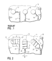
- This invention relates to packaging of semiconductor chips and more particularly to line-to-via connections in ceramic packaging structures.
- the conductor lines are being narrowed in an attempt to maximize the use of space on the package to increase the density of the package.
- a multilayered ceramic package 10 has a set of vias 11, 12, 13 connected in turn to lines 14, 15, 16 with conductor lines 14-16 being very narrow, i.e. only about 76pm (3mils) wide.
- the vias are far larger in width than the conductor lines and a problem of cracking at the junction or interface between the line and the via leads to open circuits to an undesirable degree.
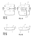
- FIG. 3A is a plan view of a segment of the prior art package of FIG. 1 rotated 90°.
- FIG. 3B is a section of FIG. 3A taken along line 3B-3B showing the thickness of prior art line-to-via connections.
- FIG. 3A and FIG. 3B show a fragment of the plan and sectional schematics of the package FIG. 1 with one of the prior art line to via connections of FIG. 1.
- the via 12 of FIG. 1 is connected in turn to line 14 with conductor lines 15 being thin, having a thickness t 1 only about 12wm (0.5 mil) thick.
- a semiconductor ceramic packaging substrate has vias of sintered electrically conductive metal therethrough and metal conductive elements on the surface thereof.
- the vias are connected to the conductive elements in a predetermined pattern.
- the improvement comprises a via having a conductive cap on the surface thereof.
- the conductive cap joins the via and the conductive element.
- the cap has a width substantially larger than the diameter of the vias at the point of contact of each of the vias and the associated conductor in contact therewith.
- a semiconductor glass ceramic packaging substrate has vias of sintered electrically conductive metal therethrough and metal conductive elements on the surface thereof.
- the vias are connected to the conductive elements in a predetermined pattern.
- the improvement comprises the via having a conductive cap on the surface thereof.
- the cap joins the via and the conductive element.
- the conductive cap has a width on the order of 1.5 to 2 times the diameter of the vias at the point of contact of each of the vias and the associated conductor in contact therewith.
- the vias are connected to the conductive elements in a predetermined pattern.
- the improvement comprises a conductive via cap on the surface of the via.
- the via cap has a cross sectional area substantially larger than the cross sectional area of the conductive element at the point of contact of the via cap and the conductive element in contact therewith.
- a semiconductor ceramic packaging substrate has the usual vias of sintered electrically conductive metal extending through the substrate.
- Each via is connected to the conductive elements in a predetermined pattern through a conductive via cap on the surface of the ceramic package.
- the caps join each conductive element and each via.
- the cap has a width substantially larger than the diameter of the via at the point of contact of the via and the conductive element in contact with it.
- the caps are also substantially thicker and wider than the conductive elements.
- a multilayered ceramic package 20 has a set of vias 21, 22, 23 indicated by the dotted lines (in phantom) connected in turn to lines 24, 25, 26 with conductor lines 24-26 being very narrow, i.e. only about 76 m (3 mils) wide.
- the new via caps 27-29 provided in accordance with this invention at the via ends of conductor lines 24-26 respectively are considerably wider than the conductor lines 24-26.
- the vias 21, 22, 23 are far narrower (less wide) than the via caps 27-29 of conductor lines 24-26 respectively. Accordingly, as a result of the thicker structure at the cap the problem of cracking at the junction or interface between a line and the corresponding via no longer leads to open circuits to any considerable degree.
- the line-to-via connection is redesigned to provide a thick paste deposit and a large cross sectional area both in the vicinity of the line-to-via junction, and at the line-to-via junction to reduce latent and actual open defects.
- the length of the enlarged via caps 27-29 of the conductor lines preferably have a line-offset-segment length X and a via cap diameter y which have a relationship as follows:
- FIG. 4A is a plan view of a segment of the package of FIG. 2.
- FIG. 4B is a section of FIG. 4A taken along line 4B-4B showing the thickness of line-to-via connections employed in the embodiment of this invention shown in FIG. 2.
- FIGS. 4A and 4B the portion of the multilayered ceramic package 20 including vias 21 and via cap 27 is shown.
- Via cap 27 is connected to line 24, but conductor lines 24 is thinner, i.e. only about 12wm (.05 mils) thick.
- the via cap 27 which is about 25 ⁇ m-50m (1-2mils) thick 24 is considerably thicker than the conductor line 24 which is about 12wm (0.5mils) thick. As the via cap 27 (as well as caps 28 and 29, etc.) is so thick, the problem of cracking at the junction or interface between line 24 and the corresponding via 21 no longer leads to open circuits to nearly the same degree.
- the parameters of the circuits of FIGS. 4A and 4B have important relationships, as described above.
- the parameters are as follows:
Landscapes
- Engineering & Computer Science (AREA)
- Microelectronics & Electronic Packaging (AREA)
- Physics & Mathematics (AREA)
- Condensed Matter Physics & Semiconductors (AREA)
- General Physics & Mathematics (AREA)
- Computer Hardware Design (AREA)
- Power Engineering (AREA)
- Printing Elements For Providing Electric Connections Between Printed Circuits (AREA)
- Production Of Multi-Layered Print Wiring Board (AREA)
- Electric Connection Of Electric Components To Printed Circuits (AREA)
- Internal Circuitry In Semiconductor Integrated Circuit Devices (AREA)
Applications Claiming Priority (2)
| Application Number | Priority Date | Filing Date | Title |
|---|---|---|---|
| US92153992A | 1992-07-29 | 1992-07-29 | |
| US921539 | 1992-07-29 |
Publications (2)
| Publication Number | Publication Date |
|---|---|
| EP0581712A2 true EP0581712A2 (fr) | 1994-02-02 |
| EP0581712A3 EP0581712A3 (fr) | 1994-04-06 |
Family
ID=25445587
Family Applications (1)
| Application Number | Title | Priority Date | Filing Date |
|---|---|---|---|
| EP93480075A Withdrawn EP0581712A2 (fr) | 1992-07-29 | 1993-06-15 | Configuration de conducteurs décalés sur substrats céramiques multicouches pour éviter des craquelures entre lignes conductrices et traversées |
Country Status (3)
| Country | Link |
|---|---|
| US (1) | US5446246A (fr) |
| EP (1) | EP0581712A2 (fr) |
| JP (1) | JP2559977B2 (fr) |
Cited By (2)
| Publication number | Priority date | Publication date | Assignee | Title |
|---|---|---|---|---|
| WO2000022894A1 (fr) * | 1998-10-13 | 2000-04-20 | Sun Microsystems, Inc. | Appareil et systeme offrant plus d'options de traces du signal lors de l'encapsulation de cablages imprimes et de circuits integres |
| US7143327B2 (en) | 2002-10-30 | 2006-11-28 | Stmicroelectronics, S.R.L. | Method and system for compressing repetitive data, in particular data used in memory device testing |
Families Citing this family (7)
| Publication number | Priority date | Publication date | Assignee | Title |
|---|---|---|---|---|
| US5539156A (en) * | 1994-11-16 | 1996-07-23 | International Business Machines Corporation | Non-annular lands |
| US8097471B2 (en) * | 2000-11-10 | 2012-01-17 | 3M Innovative Properties Company | Sample processing devices |
| US7323142B2 (en) * | 2001-09-07 | 2008-01-29 | Medtronic Minimed, Inc. | Sensor substrate and method of fabricating same |
| AU2002331796A1 (en) * | 2001-09-07 | 2003-03-24 | Medtronic Minimed, Inc. | Sensor substrate and method of fabricating same |
| US7101343B2 (en) * | 2003-11-05 | 2006-09-05 | Temple University Of The Commonwealth System Of Higher Education | Implantable telemetric monitoring system, apparatus, and method |
| WO2015048808A1 (fr) * | 2013-09-30 | 2015-04-02 | Wolf Joseph Ambrose | Pâte d'argent formant un film épais scellée hermétiquement par un film mince multicouche superficiel |
| CN107799494A (zh) * | 2017-11-03 | 2018-03-13 | 北方电子研究院安徽有限公司 | Ltcc超多层生瓷直通孔版图设计及制造工艺 |
Citations (4)
| Publication number | Priority date | Publication date | Assignee | Title |
|---|---|---|---|---|
| EP0045877A1 (fr) * | 1980-08-11 | 1982-02-17 | International Business Machines Corporation | Assemblage de plaquettes à circuit imprimé à lames céramiques comprenant des moyens capacitifs |
| EP0145599A2 (fr) * | 1983-12-08 | 1985-06-19 | Eurofarad Efd | Substrat d'interconnexion en alumine pour composant électronique, et procédé pour sa fabrication |
| EP0165427A2 (fr) * | 1984-05-21 | 1985-12-27 | International Business Machines Corporation | Substrat d'empaquetage pour semi-conducteur et procédé de fabrication |
| US4695403A (en) * | 1985-06-17 | 1987-09-22 | Matsushita Electric Industrial Co., Ltd. | Thick film conductor composition |
Family Cites Families (15)
| Publication number | Priority date | Publication date | Assignee | Title |
|---|---|---|---|---|
| US3335489A (en) * | 1962-09-24 | 1967-08-15 | North American Aviation Inc | Interconnecting circuits with a gallium and indium eutectic |
| US3571923A (en) * | 1968-12-30 | 1971-03-23 | North American Rockwell | Method of making redundant circuit board interconnections |
| US3859711A (en) * | 1973-03-20 | 1975-01-14 | Ibm | Method of detecting misregistration of internal layers of a multilayer printed circuit panel |
| US4340436A (en) * | 1980-07-14 | 1982-07-20 | International Business Machines Corporation | Process for flattening glass-ceramic substrates |
| JPS5745259A (en) * | 1980-09-01 | 1982-03-15 | Hitachi Ltd | Resin sealing type semiconductor device |
| JPS6153792A (ja) * | 1984-08-23 | 1986-03-17 | 株式会社東芝 | 多層配線基板 |
| CA1249064A (fr) * | 1987-07-06 | 1989-01-17 | Reginald B.P. Bennett | Methode d'application de conducteurs de recouvrement sur la surface d'une carte de circuits imprimes |
| JPH01300594A (ja) * | 1988-05-28 | 1989-12-05 | Fujitsu Ltd | 超伝導セラミックスを用いた多層基板の製造方法 |
| EP0382203B1 (fr) * | 1989-02-10 | 1995-04-26 | Fujitsu Limited | Empaquetage céramique du type dispositif semi-conducteur et procédé pour son assemblage |
| JPH02267995A (ja) * | 1989-04-07 | 1990-11-01 | Ngk Insulators Ltd | 多層回路基板およびその製造方法 |
| JP2810143B2 (ja) * | 1989-09-13 | 1998-10-15 | 株式会社日立製作所 | 厚膜薄膜混成多層配線基板 |
| JPH03154395A (ja) * | 1989-11-13 | 1991-07-02 | Sumitomo Electric Ind Ltd | 回路基板およびその製造方法 |
| JPH03244189A (ja) * | 1990-02-21 | 1991-10-30 | Fujitsu Ltd | セラミック配線板のビア導体接続方法 |
| JPH04357898A (ja) * | 1991-06-04 | 1992-12-10 | Toshiba Corp | セラミックス基板 |
| JPH06112355A (ja) * | 1992-09-29 | 1994-04-22 | Toshiba Corp | セラミックパッケージ |
-
1993
- 1993-06-10 JP JP5138375A patent/JP2559977B2/ja not_active Expired - Fee Related
- 1993-06-15 EP EP93480075A patent/EP0581712A2/fr not_active Withdrawn
-
1994
- 1994-01-24 US US08/186,227 patent/US5446246A/en not_active Expired - Fee Related
Patent Citations (4)
| Publication number | Priority date | Publication date | Assignee | Title |
|---|---|---|---|---|
| EP0045877A1 (fr) * | 1980-08-11 | 1982-02-17 | International Business Machines Corporation | Assemblage de plaquettes à circuit imprimé à lames céramiques comprenant des moyens capacitifs |
| EP0145599A2 (fr) * | 1983-12-08 | 1985-06-19 | Eurofarad Efd | Substrat d'interconnexion en alumine pour composant électronique, et procédé pour sa fabrication |
| EP0165427A2 (fr) * | 1984-05-21 | 1985-12-27 | International Business Machines Corporation | Substrat d'empaquetage pour semi-conducteur et procédé de fabrication |
| US4695403A (en) * | 1985-06-17 | 1987-09-22 | Matsushita Electric Industrial Co., Ltd. | Thick film conductor composition |
Non-Patent Citations (1)
| Title |
|---|
| HARPER 'Electronic Packaging and Interconnection Handbook' 1991 , MCGRAW-HILL , NEW YORK,US * page 7.58, paragraph 1-2; figure 7.30 * * |
Cited By (3)
| Publication number | Priority date | Publication date | Assignee | Title |
|---|---|---|---|---|
| WO2000022894A1 (fr) * | 1998-10-13 | 2000-04-20 | Sun Microsystems, Inc. | Appareil et systeme offrant plus d'options de traces du signal lors de l'encapsulation de cablages imprimes et de circuits integres |
| US6534872B1 (en) | 1998-10-13 | 2003-03-18 | Sun Microsystems, Inc. | Apparatus and system with increased signal trace routing options in printed wiring boards and integrated circuit packaging |
| US7143327B2 (en) | 2002-10-30 | 2006-11-28 | Stmicroelectronics, S.R.L. | Method and system for compressing repetitive data, in particular data used in memory device testing |
Also Published As
| Publication number | Publication date |
|---|---|
| JP2559977B2 (ja) | 1996-12-04 |
| JPH0697314A (ja) | 1994-04-08 |
| US5446246A (en) | 1995-08-29 |
| EP0581712A3 (fr) | 1994-04-06 |
Similar Documents
| Publication | Publication Date | Title |
|---|---|---|
| US5502337A (en) | Semiconductor device structure including multiple interconnection layers with interlayer insulating films | |
| EP0499063B1 (fr) | Circuit intégré semi-conducteur encapsulé en résine comprenant une couche conductrice | |
| US4021838A (en) | Semiconductor integrated circuit devices | |
| US5869357A (en) | Metallization and wire bonding process for manufacturing power semiconductor devices | |
| US4766479A (en) | Low resistance electrical interconnection for synchronous rectifiers | |
| EP0581712A2 (fr) | Configuration de conducteurs décalés sur substrats céramiques multicouches pour éviter des craquelures entre lignes conductrices et traversées | |
| US5994763A (en) | Wiring structure for semiconductor element and method for forming the same | |
| US5245210A (en) | MOS type semiconductor device | |
| KR19990072029A (ko) | 마이크로웨이브 하이브리드 집적회로 | |
| US5465007A (en) | High frequency transistor with reduced parasitic inductance | |
| JP3696706B2 (ja) | 半導体装置の電源線構造 | |
| JPH01225137A (ja) | 半導体集積回路装置 | |
| US5021869A (en) | Monolithic semiconductor chip interconnection technique and arrangement | |
| US20040065944A1 (en) | Semiconductor device | |
| JPS5854646A (ja) | 混成集積回路装置 | |
| JPH02183536A (ja) | 半導体装置 | |
| KR200309911Y1 (ko) | 다층 배선 | |
| JPS63124539A (ja) | 混成集積回路 | |
| JPH01128448A (ja) | 半導体装置の配線接続部 | |
| JPH04188753A (ja) | 多層配線半導体装置 | |
| JPS59208750A (ja) | 半導体装置の配線構造 | |
| JPS63301544A (ja) | スタンダ−ドセル方式の半導体集積回路 | |
| JP2559977C (fr) | ||
| US20050067669A1 (en) | Fuse circuit and semiconductor device including the same | |
| JPH0582659A (ja) | バイアホール構造を用いた配線構造 |
Legal Events
| Date | Code | Title | Description |
|---|---|---|---|
| PUAI | Public reference made under article 153(3) epc to a published international application that has entered the european phase |
Free format text: ORIGINAL CODE: 0009012 |
|
| AK | Designated contracting states |
Kind code of ref document: A2 Designated state(s): DE FR GB |
|
| PUAL | Search report despatched |
Free format text: ORIGINAL CODE: 0009013 |
|
| AK | Designated contracting states |
Kind code of ref document: A3 Designated state(s): DE FR GB |
|
| STAA | Information on the status of an ep patent application or granted ep patent |
Free format text: STATUS: THE APPLICATION IS DEEMED TO BE WITHDRAWN |
|
| 18D | Application deemed to be withdrawn |
Effective date: 19941007 |