EP0566145A2 - Tiefpass-Hochfrequenzfilter - Google Patents
Tiefpass-Hochfrequenzfilter Download PDFInfo
- Publication number
- EP0566145A2 EP0566145A2 EP93106243A EP93106243A EP0566145A2 EP 0566145 A2 EP0566145 A2 EP 0566145A2 EP 93106243 A EP93106243 A EP 93106243A EP 93106243 A EP93106243 A EP 93106243A EP 0566145 A2 EP0566145 A2 EP 0566145A2
- Authority
- EP
- European Patent Office
- Prior art keywords
- dielectric layer
- electrode
- strip line
- pass filter
- frequency low
- Prior art date
- Legal status (The legal status is an assumption and is not a legal conclusion. Google has not performed a legal analysis and makes no representation as to the accuracy of the status listed.)
- Granted
Links
- 239000003990 capacitor Substances 0.000 claims description 34
- 238000010586 diagram Methods 0.000 description 4
- 239000000758 substrate Substances 0.000 description 4
- 239000000919 ceramic Substances 0.000 description 3
- 239000002003 electrode paste Substances 0.000 description 3
- 230000003071 parasitic effect Effects 0.000 description 3
- 238000005259 measurement Methods 0.000 description 2
- 230000003247 decreasing effect Effects 0.000 description 1
- 230000001939 inductive effect Effects 0.000 description 1
- 238000003780 insertion Methods 0.000 description 1
- 230000037431 insertion Effects 0.000 description 1
Images


Classifications
-
- H—ELECTRICITY
- H01—ELECTRIC ELEMENTS
- H01P—WAVEGUIDES; RESONATORS, LINES, OR OTHER DEVICES OF THE WAVEGUIDE TYPE
- H01P1/00—Auxiliary devices
- H01P1/20—Frequency-selective devices, e.g. filters
- H01P1/201—Filters for transverse electromagnetic waves
- H01P1/203—Strip line filters
- H01P1/2039—Galvanic coupling between Input/Output
Definitions
- the present invention relates to a high-frequency low-pass filter and more particularly to the high-frequency low-pass filter having a strip line electrode for using as an inductor.
- Fig. 15 is a perspective view showing an example of a conventional high-frequency low-pass filter.
- the high-frequency low-pass filter 1 shown in Fig. 15 includes a dielectric substrate 2. On whole one main surface of the dielectric substrate 2, an earth electrode 3 is formed. On center of the other main surface of the dielectric substrate 2, two microstrip line electrodes 4a and 4b as a first and a second inductors are formed.
- a first capacitive open-circuited stub electrode 5a as a part of a first capacitor and an input electrode 6a as an input terminal are formed extending from one end of one microstrip line electrode 4a
- a second capacitive open-circuited stub electrode 5b as a part of a second capacitor is formed extending from the other end of one microstrip line electrode 4a and one end of the other microstrip line electrode 4b
- a third capacitive open-circuited stub electrode 5c as a part of a third capacitor and an output electrode 6b as an output terminal are formed extending from the other end of the other microstrip line electrode 4b.
- Fig. 16 is a perspective view showing another example of a conventional high-frequency low-pass filter. Compared with the high-frequency low-pass filter shown in Fig. 15, in the high-frequency low-pass filter 1 shown in Fig. 16, three chip capacitors 7a, 7b and 7c instead of three capacitive open-circuited stub electrodes are used.
- the high-frequency low-pass filters 1 shown in Fig. 15 and Fig. 16 have an equivalent circuit shown in Fig. 17 in a form of concentrated constant, respectively. That is, the high-frequency low-pass filters 1 shown in Fig. 15 and Fig. 16 have an input terminal IN and an output terminal OUT, respectively. Between the input terminal IN and the output terminal OUT, the first and the second inductors L 1 and L 2 are connected in series. Furthermore, the input terminal IN is grounded through the first capacitor C, , the connecting point between the first and the second inductors L 1 and L 2 is grounded through the second capacitor C 2 , and the output terminal OUT is grounded through the third capacitor C 3 .
- an unnecessary passband is generated by resonance in the frequency on the wavelength of XN/(2 ⁇ r ) wherein X is the line length of the microstrip line electrode, E , is the relative dielectric constant around the microstrip line electrode, and N is an integral number, therefore, a good spurious characteristic is not obtained, respectively.
- a high-frequency low-pass filter is a high-frequency low-pass filter comprising a strip line electrode used as an inductor, a capacitive open-circuit stub electrode connected to the strip line electrode, and a capacitor formed between the strip line electrode and the capacitive open-circuited stub electrode and connected to the inductor in parallel, wherein the parallel resonance frequency between the inductor and the capacitor is approximately the frequency on the wavelength of X/(2 ⁇ r ) wherein X is the line length of the strip line electrode, and ⁇ r is the relative dielectric constant around the strip line electrode.
- the parallel resonance frequency between the inductor and the capacitor is approximately the frequency on the wavelength of X/(2 ⁇ r ) wherein X is the line length of the strip line elctrode, and ⁇ r is the relative dielectric constant around the strip line electrode, an unnecessary passband by resonance in the frequency on the wavelength of XN/(2 ⁇ r ) wherein N is an integral number is suppressed.
- a spurious characteristic is improved.
- a high-frequency low-pass filter having a good spurious characteristic is obtained.
- the strip line electrode is used as the inductor and the capacitive open-circuited stub electrode is used, it can be formed in a laminated structure, therefore, it can be miniaturized, it can be manufactured as a surface mount device.
- Another high-frequency low-pass filter is a high-frequency low-pass filter comprising a first dielectric layer, an earth electrode formed on the first dielectric layer, a second dielectric layer formed on the first dielectric layer and sandwiching the earth electrode between the first dielectric layer and the second dielectric layer, a capacitive open-circuited stub electrode formed on the second dielectric layer and opposite to the earth electrode, a third dielectric layer formed on the second dielectric layer and sandwiching the capacitive open-circuited stub electrode between the second dielectric layer and the third dielectric layer, and two strip line electrodes formed on the third dielectric layer and connected to the capacitive open-circuited stub electrode, wherein the surface areas of the two strip line electrodes are different from each other.
- a capacitance is formed between the earth electrode and the capacitive open-circuited stub electrode. Furthermore, two inductances are formed by the two strip line electrodes.
- the high-frequency low-pass filter is made by the inductances and the capacitance.
- a capacitance formed between one strip line electrode and other electrodes is different from a capacitance formed between the other strip line electrode and the other electrodes. Consequently, resonance points generated in a high frequency band are different each other and hence do not overlap with each other.
- the high-frequency low-pass filter provides a preferable frequency characteristic.
- Fig. 1 is a perspective view showing a high-frequency low-pass filter according to an embodiment of the present invention.
- the high-frequency low-pass filter 10 includes a laminate 11 which is, for example, 5.7mm wide, 5.0mm long, and 2.0mm thick.
- the laminate 11 includes a first dielectric layer 12.
- An earth electrode 14 is formed on the entire surface of the first dielectric layer 12 except the periphery thereof.
- Six drawing terminals 16a, 16b, 16c, 16d, 16e and 16f are formed in the direction from the earth electrode 14 toward the edges of the first dielectric layer 12.
- the drawing terminals 16a and 16b are formed in the direction from the earth electrode 14 toward one edge of the first dielectric layer 12 with a distance between the drawing terminals 16a and 16b.
- the drawing terminals 16c and 16d are formed in the direction from the earth electrode 14 toward the opposite edge of the first dielectric layer 12 with a short distance between both drawing terminals 16c and 16d in the vicinity of the center of the edge.
- the drawing terminals 16e and 16f are formed in the directions from the earth electrode 14 toward the another opposite edges of the first dielectric layer 12.
- a second dielectric layer 18 is laminated on the earth electrode 14.
- a first capacitive open-circuited stub electrode 20, a second capacitive open-circuited stub electrode 22 and a third capacitive open-circuited stub electrode 24 which comprise a part of first, second and third capacitors are formed on the second dielectric layer 18.
- the second capacitive open-circuited stub electrode 22 is formed in the vicinity of the center of one edge of the second dielectric layer 18.
- the first capacitive open-circuited stub electrode 20 and the third capacitive open-circuited stub electrode 24 are formed in the vicinity of the other edge of the second dielectric layer 18 with a distance therebetween.
- the first, second, and third capacitive open-circuited stub electrodes 20, 22, and 24 are opposite to the earth electrode 14.
- Two connecting terminals 22a and 22b are formed in the direction from the second capacitive open-circuited stub electrode 22 toward one edge of the second dielectric layer 18.
- the connecting terminals 22a and 22b are formed in the vicinity of the center of the edge of the second dielectric layer 18 with a short distance therebetween.
- Connecting terminals 20a and 24a are formed in the direction from the first and third capacitive open-circuited stub electrodes 20 and 24 toward the other edge of the second dielectric layer 18 with a distance therebetween.
- a third dielectric layer 26 is laminated on the first, second and third capacitive open-circuited stub electrodes 20, 22 and 24.
- a first strip line electrode 28 and a second strip line electrode 30 which are used as first and second inductors are formed on the third dielectric layer 26.
- the first and second strip line electrodes 28 and 30 are formed as meander lines in the direction from one edge of the third dielectric layer 26 toward the other edge thereof. In this case, a portion of the first strip line electrode 28 is formed opposite to the first and the second capacitive open-circuited stub electrodes 20 and 22, for forming a capacitor which is parallel resonated with the inductor of the first strip line electrode 28.
- a portion of the second strip line electrode 30 is formed opposite to the second and the third capacitive open-circuited stub electrodes 22 and 24, for forming a capacitor which is parallel resonated with the inductor of the second strip line electrode 30.
- One end 28a of the first strip line electrode 28 is formed at a position corresponding to the position of the connecting terminal 22a of the second capacitive open-circuited stub electrode 22, and the other end 28b of the first strip line electrode 28 is formed at a position corresponding to the position of the connecting terminal 20a of the first capacitive open-circuited stub electrode 20.
- One end 30a of the second strip line electrode 30 is formed at a position corresponding to the position of the connecting terminal 22b of the second capacitive open-circuited stub electrode 22, and the other end 30b of the second strip line electrode 30 is formed at a position corresponding to the position of the connecting terminal 24a of the third capacitive open-circuited stub electrode 24.
- a fourth dielectric layer 32 is laminated on the first strip line electrode 28 and the second strip line electrode 30.
- a shield electrode 34 is formed on the entire surface of the fourth dielectric layer 32 except the periphery thereof.
- Six drawing terminals 36a, 36b, 36c, 36d, 36e and 36f are formed in the direction from the shield electrode 34 toward edges of the fourth dielectric layer 32.
- the drawing terminals 36a and 36b are formed in the direction from the shield electrode 34 toward one edge of the fourth dielectric layer 32 with a distance therebetween.
- the drawing terminals 36c and 36d are formed in the direction from the shield electrode 34 toward the other edge of the fourth dielectric layer 32 with a short distance therebetween in the vicinity of the center of the edge.
- the drawing terminals 36e and 36f are formed in the directions from the shield electrode 34 toward the another opposite edges of the fourth dielectric layer 32.
- a fifth dielectric layer 38 is laminated on the shield electrode 34.
- Ten outer electrodes 40a, 40b, 40c, 40d, 40e, 40f, 40g, 40h, 40i, and 40j are formed on sides of the laminate 11 as shown in Fig. 1.
- the four outer electrodes 40a-40d are formed on one side of the laminate 11 while the other four outer electrodes 40e-40h are formed on the other side thereof.
- the outer electrodes 40i and 40j are formed on another opposite sides of the laminate 11.
- the outer electrodes 40a-40j are formed from the upper surface to the lower surface via the side surface of the laminate 11.
- the outer electrodes 40a, 40d, 40f, 40g, 40i and 40j are connected to the drawing terminals 16a, 16b, 16c, 16d, 16e and 16f of the earth electrode 14 respectively, and connected to the drawing terminals 36a, 36b, 36c, 36d, 36e and 36f of the shield electrode 34 respectively.
- the outer electrode 40b is connected to one end 28a of the first strip line electrode 28 and the connecting terminal 22a of the second capacitive open-circuited stub electrode 22.
- the outer electrode 40e is connected to the other end 28b of the first strip line electrode 28 and the connecting terminal 20a of the first capacitive open-circuited stub electrode 20.
- the outer electrode 40c is connected to one end 30a of the second strip line electrode 30 and the connecting terminal 22b of the second capacitive open-circuited stub electrode 22.
- the outer electrode 40h is connected to the other end 30b of the second strip line electrode 30 and the connecting terminal 24a of the third capacitive open-circuited stub electrode 24.
- the high-frequency low-pass filter 10 is formed as follows: Electrode paste is applied to each dielectric ceramic green sheet in the configuration of each electrode and each terminal and baked with dielectric ceramic green sheets laminated one on the other. At this time, the number of the ceramic green sheets is adjusted according to the thickness of each dielectric layer. In order to form the outer electrodes, the raw laminate on which the electrode paste has been applied is baked together, or sintered laminate on which the electrode paste is applied is baked.
- the high-frequency low-pass filter 10 has an equivalent circuit comprising first and second inductors L 1 and L 2 and first, second, and third capacitors Ci, C 2 , and C 3 connected with each other in a ladder-type. Meanwhile, between the first, the second and the third capacitors C 1 C 2 and C 3 and the earth potential, parasitic inductances L 11 ,L 12 and L 13 based on the earth electrode 14 and so on are generated, respectively.
- stray capacitance Co and a parasitic inductance Lo are generated in series
- stray capacitance C o2 and a parasitic inductance Lo 2 are generated in series.
- the stray capacitance C 01 is generated between the first strip line electrode 28 and other electrodes such as the earth electrode 14 and the shield electrode 34.
- the stray capacitance C o2 is generated between the second strip line electrode 30 and other electrodes such as the earth electrode 14 and the shield electrode 34.
- a capacitor C 11 is connected to the first inductor L 1 in parallel
- a capacitor C12 is connected to the second inductor L 2 in parallel.
- the capacitance of one capacitor C 11 is selected so as to approximately coincide the parallel resonance frequency between the first inductor L 1 and the capacitor C 11 with the frequency on the wavelength of X/(2 ⁇ r ) wherein ⁇ is the line length of the first inductor L 1 (the first strip line electrode 28), and ⁇ r is the relative dielectric constant around the first strip line electrode 28.
- the capacitance of the other capacitor C 1 2 is selected so as to approximately coincide the parallel resonance frequency between the second inductor L 2 and the capacitor C 12 with the frequency on the wavelength of X/(2 ⁇ r ) wherein ⁇ is the line length of the second inductor L 2 (the second strip line electrode 30), and ⁇ r is the relative dielectric constant around the second strip line electrode 30.
- the capacitance of the capacitor C 11 can be controlled by changing the thickness of the third dielectric layer 26, an opposite surface area or an opposite distance between the first and the second capacitive open-circuited stub electrodes 20 and 22 and the first strip line electrode 28.
- the thickness of the third dielectric layer 28 is thin, the capacitance is great.
- the opposite surface area between the first and the second capacitive open-circuited stub electrodes 20 and 22 and the first strip line electrode 28 is great, the capacitance is great.
- configurations or positions of these electrodes may be changed.
- the capacitance of the other capacitor C 12 can be controlled by changing the thickness of the third dielectric layer 28, the opposite surface area or the opposite distance between the second and the third capacitive open-circuited stub electrodes 22 and 24.
- each parallel resonance frequency is not the frequency on the wavelength of XN/(2 ⁇ r ) associated with each strip line electrode in the embodiment.
- the frequency characteristics of the embodiment and the comparison example are shown in Fig 4 and Fig. 5, respectively.
- the electrodes 20, 22 and 24 work a notch filter in the frequency on 1/4 wavelength of the length thereof, an attenuation pole is generated in the frequency, respectively.
- these frequencies are shifted into an integral times cutoff frequency, the attenuation by higher harmonic of the cutoff frequency can be increased.
- the present invention is applied to a high-frequency low-pass filter having one, three or more parallel resonance circuits, too.
- the parallel resonance frequency between the inductor of the strip line electrode and the capacitor may be approximately the frequency on the wavelength of X/(2 ⁇ r) associated with the strip line electrode wherein X is the line length of the strip line electrode, and E , is the relative dielectric constant around the strip line electrode.
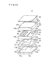
- Fig. 6 is an exploded perspective view showing a laminate of another embodiment of the present invention. Compared with the embodiment shown in Fig. 1 through Fig. 4, in the embodiment used the laminate shown in Fig. 6, the length of the first strip line electrode 28 is different from that of the second strip line electrode 30.
- the capacitor C 11 produces an unnecessary resonance point in a high frequency band which is the resonance frequency associated with the first inductor L 1 .
- the capacitor C 12 produces an unnecessary resonance point in a high-frequency band which is the resonance frequency associated with the second inductor L 2 .
- the length of the first strip line electrode 28 is different from that of the second strip line electrode 30. Consequently, there is a difference between the capacitance of the capacitors C 11 and Ci2. As a result, the frequencies at the resonance points have divergence and thus the resonance points do not overlap with each other in the same frequency. Accordingly, the generation of spurious response can be suppressed in some degree.
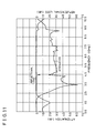
- the attenuation becomes approximately 14 dB at a frequency of approximately 4.4 GHz as shown in Fig. 7.
- the attenuation becomes approximately 17 dB at a frequency of approximately 4.4 GHz as shown in Fig. 12.
- frequency characteristic having a small amount of spurious response can be obtained by differentiating the length of the first strip line electrode 28 and that of the second strip line electrode 30 from each other.
- Fig. 13 is an exploded perspective view showing a modified example of the laminate shown in Fig. 6.
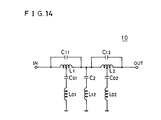
- Fig. 14 is an equivalent circuit diagram of the high-frequency low-pass filter used the laminate shown in Fig. 13.
- the earth electrode 14 is not opposite to the first capacitive open-circuited stub electrode 20 and the third capacitive open-circuited stub electrode 24, and the capacitors C 1 and C 3 are not formed. It is possible that the capacitors C 1 and C 3 are not formed.
- the width of the first strip line electrode 28 and that of the second strip line electrode 30 may be differentiated from each other instead of differentiating the length of the first strip line electrode 28 and that of the second strip line electrode 30 from each other. That is, the opposite area between the first strip line electrode 28 and the other electrodes is different from the opposite area between the second strip line electrode 30 and the other electrodes by differentiating the width of the first strip line electrode 28 from that of the second strip line electrode 30.
- the capacitance to be formed between the first strip line electrode 28 and the other electrodes is different from the capacitance to be formed between the second strip line electrode 30 and the other electrodes. Furthermore, in each of the embodiments, it is possible to adjust the capacitance by changing the opposite distance between the strip line electrode and the capacitive open-circuited stub electrode.
- the high-frequency low-pass filter has two strip line electrodes, but it may comprise three or more strip line electrodes. In this case, the surface areas of all strip line electrodes are differentiated from each other.
- the high-frequency low-pass filter is as small as 5.7mm x 5.0mm x 2.0mm and has a small spurious response.
- insertion loss in a passband is less than 0.6 dB and the attenuation more than 20 dB can be secured in the range from the passband until 9 GHz.
- a microstrip line electrode may be used as a strip line electrode.
Landscapes
- Physics & Mathematics (AREA)
- Electromagnetism (AREA)
- Filters And Equalizers (AREA)
- Control Of Motors That Do Not Use Commutators (AREA)
Applications Claiming Priority (6)
| Application Number | Priority Date | Filing Date | Title |
|---|---|---|---|
| JP4124178A JP3023939B2 (ja) | 1992-04-16 | 1992-04-16 | 高周波用ローパスフィルタ |
| JP124177/92 | 1992-04-16 | ||
| JP124178/92 | 1992-04-16 | ||
| JP4124177A JP2976696B2 (ja) | 1992-04-16 | 1992-04-16 | 高周波用ローパスフィルタ |
| JP355743/92 | 1992-12-17 | ||
| JP35574392A JP2773590B2 (ja) | 1992-12-17 | 1992-12-17 | ローパスフィルタ |
Publications (3)
| Publication Number | Publication Date |
|---|---|
| EP0566145A2 true EP0566145A2 (de) | 1993-10-20 |
| EP0566145A3 EP0566145A3 (de) | 1994-03-02 |
| EP0566145B1 EP0566145B1 (de) | 1998-08-26 |
Family
ID=27314877
Family Applications (1)
| Application Number | Title | Priority Date | Filing Date |
|---|---|---|---|
| EP93106243A Expired - Lifetime EP0566145B1 (de) | 1992-04-16 | 1993-04-16 | Tiefpass-Hochfrequenzfilter |
Country Status (3)
| Country | Link |
|---|---|
| US (1) | US5357227A (de) |
| EP (1) | EP0566145B1 (de) |
| DE (1) | DE69320521T2 (de) |
Cited By (6)
| Publication number | Priority date | Publication date | Assignee | Title |
|---|---|---|---|---|
| EP0675560A1 (de) * | 1994-03-29 | 1995-10-04 | Murata Manufacturing Co., Ltd. | Tiefpassfilter |
| GB2289167A (en) * | 1994-04-30 | 1995-11-08 | Ceramic Filters Ltd | Electrical filters |
| FR2828582A1 (fr) * | 2001-08-10 | 2003-02-14 | Murata Manufacturing Co | Filtre passe-bas a caracteristique plate de retard de groupe, et recepteur de signaux optiques |
| EP1503446A2 (de) * | 2003-06-30 | 2005-02-02 | Taiyo Yuden Co., Ltd. | Schaltkreis für ein Filter und laminiertes Filter |
| US7091800B2 (en) | 2001-06-21 | 2006-08-15 | Murata Manufacturing Co., Ltd. | Noise filter |
| WO2018144376A1 (en) * | 2017-02-04 | 2018-08-09 | Cts Corporation | Rf filter with separate capacitive and inductive substrates |
Families Citing this family (33)
| Publication number | Priority date | Publication date | Assignee | Title |
|---|---|---|---|---|
| US5412358A (en) * | 1992-02-28 | 1995-05-02 | Ngk Insulators, Ltd. | Layered stripline filter |
| US5910755A (en) * | 1993-03-19 | 1999-06-08 | Fujitsu Limited | Laminate circuit board with selectable connections between wiring layers |
| US5519366A (en) * | 1993-06-08 | 1996-05-21 | Murata Manufacturing Co., Ltd. | Strip line filter |
| US5506551A (en) * | 1993-07-05 | 1996-04-09 | Murata Manufacturing Co., Ltd. | Resonator and chip type filter using the resonator |
| JP2949250B2 (ja) * | 1993-08-25 | 1999-09-13 | 株式会社村田製作所 | チップ型フィルタ |
| JPH07193403A (ja) * | 1993-12-24 | 1995-07-28 | Murata Mfg Co Ltd | 共振器 |
| JPH07201592A (ja) * | 1993-12-28 | 1995-08-04 | Murata Mfg Co Ltd | 積層型lc複合部品 |
| US5834994A (en) * | 1997-01-17 | 1998-11-10 | Motorola Inc. | Multilayer lowpass filter with improved ground plane configuration |
| US5818313A (en) | 1997-01-31 | 1998-10-06 | Motorola Inc. | Multilayer lowpass filter with single point ground plane configuration |
| US5949304A (en) * | 1997-10-16 | 1999-09-07 | Motorola, Inc. | Multilayer ceramic package with floating element to couple transmission lines |
| US5923077A (en) * | 1998-02-11 | 1999-07-13 | Bourns, Inc. | Passive component integrated circuit chip |
| JP2910758B1 (ja) * | 1998-04-27 | 1999-06-23 | 株式会社村田製作所 | 積層型lc部品 |
| US6091312A (en) * | 1998-06-26 | 2000-07-18 | Industrial Technology Research Institute | Semi-lumped bandstop filter |
| US6191666B1 (en) | 1999-03-25 | 2001-02-20 | Industrial Technology Research Institute | Miniaturized multi-layer ceramic lowpass filter |
| US6208219B1 (en) | 1999-05-12 | 2001-03-27 | Samuel Singer | Broadband RF circuits with microstrips laid out in randomly meandering paths |
| JP3825998B2 (ja) * | 2001-08-20 | 2006-09-27 | シャープ株式会社 | マイクロ波ストリップ線路フィルタおよびこれを用いた高周波送信機 |
| KR100541089B1 (ko) * | 2003-10-08 | 2006-01-11 | 삼성전기주식회사 | 적층형 저역 통과 필터 |
| TWI236796B (en) * | 2004-09-02 | 2005-07-21 | Darfon Electronics Corp | Bandpass filters |
| US20060284973A1 (en) * | 2005-06-17 | 2006-12-21 | Eastman Kodak Company | Stereoscopic viewing apparatus |
| JP5038634B2 (ja) * | 2006-02-16 | 2012-10-03 | Tdk株式会社 | ノイズフィルタ及びノイズフィルタの実装構造 |
| JP2009182376A (ja) * | 2008-01-29 | 2009-08-13 | Tdk Corp | 積層型ローパスフィルタ |
| JP4530181B2 (ja) * | 2008-01-29 | 2010-08-25 | Tdk株式会社 | 積層型ローパスフィルタ |
| US9001527B2 (en) * | 2008-02-18 | 2015-04-07 | Cyntec Co., Ltd. | Electronic package structure |
| JP5658429B2 (ja) | 2008-07-03 | 2015-01-28 | ルネサスエレクトロニクス株式会社 | 回路装置 |
| TWI460918B (zh) * | 2010-07-30 | 2014-11-11 | Univ Nat Taiwan | 共模雜訊抑制電路 |
| JP2014239203A (ja) * | 2014-01-31 | 2014-12-18 | 株式会社村田製作所 | 電子部品及び電子部品の実装構造体 |
| US11071239B2 (en) | 2018-09-18 | 2021-07-20 | Avx Corporation | High power surface mount filter |
| WO2020132022A1 (en) | 2018-12-20 | 2020-06-25 | Avx Corporation | Multilayer filter including a low inductance via assembly |
| CN113228503A (zh) | 2018-12-20 | 2021-08-06 | 阿维科斯公司 | 包括高精度电感器的多层电子装置 |
| CN113228504A (zh) | 2018-12-20 | 2021-08-06 | 阿维科斯公司 | 高频多层滤波器 |
| DE112019006352T5 (de) | 2018-12-20 | 2021-08-26 | Avx Corporation | Mehrschichtfilter, umfassend einen rückführsignalreduzierungsvorsprung |
| JP7355827B2 (ja) | 2018-12-20 | 2023-10-03 | キョーセラ・エイブイエックス・コンポーネンツ・コーポレーション | 精密に制御された容量性エリアを有するコンデンサを備える多層電子デバイス |
| CN113273029B (zh) | 2018-12-20 | 2022-08-02 | 京瓷Avx元器件公司 | 包括电容器的多层滤波器和形成多层滤波器的方法 |
Citations (3)
| Publication number | Priority date | Publication date | Assignee | Title |
|---|---|---|---|---|
| DE1926501A1 (de) * | 1969-05-23 | 1970-11-26 | Siemens Ag | Tiefpassfilter fuer elektrische Schwingungen |
| DE2708241B1 (de) * | 1977-02-25 | 1978-02-09 | Siemens Ag | Hochfrequenzschaltungsanordnung mit tiefpasscharakter |
| JPS55156414A (en) * | 1979-05-25 | 1980-12-05 | Matsushita Electric Ind Co Ltd | Band pass filter |
Family Cites Families (7)
| Publication number | Priority date | Publication date | Assignee | Title |
|---|---|---|---|---|
| US2915716A (en) * | 1956-10-10 | 1959-12-01 | Gen Dynamics Corp | Microstrip filters |
| US2945195A (en) * | 1958-03-25 | 1960-07-12 | Thompson Ramo Wooldridge Inc | Microwave filter |
| US3451015A (en) * | 1966-03-21 | 1969-06-17 | Gen Dynamics Corp | Microwave stripline filter |
| US3879690A (en) * | 1974-05-06 | 1975-04-22 | Rca Corp | Distributed transmission line filter |
| JP2600918B2 (ja) * | 1989-08-16 | 1997-04-16 | 株式会社村田製作所 | バンドパスフィルタ |
| JP2662741B2 (ja) * | 1990-03-05 | 1997-10-15 | 株式会社村田製作所 | 共振器 |
| JP2725439B2 (ja) * | 1990-05-17 | 1998-03-11 | 株式会社 村田製作所 | 電子部品の周波数調整方法 |
-
1993
- 1993-04-16 US US08/048,381 patent/US5357227A/en not_active Expired - Lifetime
- 1993-04-16 EP EP93106243A patent/EP0566145B1/de not_active Expired - Lifetime
- 1993-04-16 DE DE69320521T patent/DE69320521T2/de not_active Expired - Lifetime
Patent Citations (3)
| Publication number | Priority date | Publication date | Assignee | Title |
|---|---|---|---|---|
| DE1926501A1 (de) * | 1969-05-23 | 1970-11-26 | Siemens Ag | Tiefpassfilter fuer elektrische Schwingungen |
| DE2708241B1 (de) * | 1977-02-25 | 1978-02-09 | Siemens Ag | Hochfrequenzschaltungsanordnung mit tiefpasscharakter |
| JPS55156414A (en) * | 1979-05-25 | 1980-12-05 | Matsushita Electric Ind Co Ltd | Band pass filter |
Non-Patent Citations (2)
| Title |
|---|
| IBM TECHNICAL DISCLOSURE BULLETIN. vol. 5, no. 2 , July 1962 , NEW YORK US page 21 J.J. LENTZ 'Transmission line m-derived section' * |
| PATENT ABSTRACTS OF JAPAN vol. 5, no. 30 (E-47)(702) 24 February 1981 & JP-A-55 156 414 (MATSUSHITA DENKI SANGYO K.K.) 5 December 1980 * |
Cited By (12)
| Publication number | Priority date | Publication date | Assignee | Title |
|---|---|---|---|---|
| EP0675560A1 (de) * | 1994-03-29 | 1995-10-04 | Murata Manufacturing Co., Ltd. | Tiefpassfilter |
| US5668511A (en) * | 1994-03-29 | 1997-09-16 | Murata Manufacturing Co., Ltd. | Low-pass filter |
| GB2289167A (en) * | 1994-04-30 | 1995-11-08 | Ceramic Filters Ltd | Electrical filters |
| US7091800B2 (en) | 2001-06-21 | 2006-08-15 | Murata Manufacturing Co., Ltd. | Noise filter |
| FR2828582A1 (fr) * | 2001-08-10 | 2003-02-14 | Murata Manufacturing Co | Filtre passe-bas a caracteristique plate de retard de groupe, et recepteur de signaux optiques |
| US6791434B2 (en) | 2001-08-10 | 2004-09-14 | Murata Manufacturing Co., Ltd. | Flat group-delay low-pass filter, mounting structure thereof, flat group-delay low-pass filter device, and optical signal receiver |
| EP1503446A2 (de) * | 2003-06-30 | 2005-02-02 | Taiyo Yuden Co., Ltd. | Schaltkreis für ein Filter und laminiertes Filter |
| EP1503446A3 (de) * | 2003-06-30 | 2005-03-23 | Taiyo Yuden Co., Ltd. | Schaltkreis für ein Filter und laminiertes Filter |
| WO2018144376A1 (en) * | 2017-02-04 | 2018-08-09 | Cts Corporation | Rf filter with separate capacitive and inductive substrates |
| CN110235302A (zh) * | 2017-02-04 | 2019-09-13 | Cts公司 | 具有单独的电容和电感衬底的射频滤波器 |
| US10680302B2 (en) | 2017-02-04 | 2020-06-09 | Cts Corporation | RF filter with separate capacitive and inductive substrates |
| CN110235302B (zh) * | 2017-02-04 | 2021-10-19 | Cts公司 | 具有单独的电容和电感衬底的射频滤波器 |
Also Published As
| Publication number | Publication date |
|---|---|
| EP0566145B1 (de) | 1998-08-26 |
| DE69320521T2 (de) | 1999-02-25 |
| US5357227A (en) | 1994-10-18 |
| DE69320521D1 (de) | 1998-10-01 |
| EP0566145A3 (de) | 1994-03-02 |
Similar Documents
| Publication | Publication Date | Title |
|---|---|---|
| EP0566145B1 (de) | Tiefpass-Hochfrequenzfilter | |
| US5479141A (en) | Laminated dielectric resonator and dielectric filter | |
| US4754242A (en) | Resonator | |
| US4714906A (en) | Dielectric filter with variable central frequency | |
| JPS63171011A (ja) | バンドパスフイルタ | |
| KR0141975B1 (ko) | 절연된 필터 단을 갖는 다단 모노리딕식 세라믹 대역 소거 필터 | |
| JPH11136002A (ja) | 誘電体フィルタ及び誘電体フィルタの通過帯域特性を調整する方法 | |
| US20030129957A1 (en) | Multilayer LC filter | |
| JP2890985B2 (ja) | バンドパスフィルタ | |
| JP3023939B2 (ja) | 高周波用ローパスフィルタ | |
| JP2773590B2 (ja) | ローパスフィルタ | |
| JP2920715B2 (ja) | 高周波用ローパスフィルタ | |
| GB2302453A (en) | Dielectric filter | |
| JP2976696B2 (ja) | 高周波用ローパスフィルタ | |
| JP2666092B2 (ja) | 誘電体フィルタ | |
| US20230327632A1 (en) | Filter and multiplexer | |
| JP2737063B2 (ja) | ストリップラインフィルタ | |
| JPH08335803A (ja) | フィルタ | |
| JPH06334412A (ja) | 誘電体積層共振器および誘電体フィルタ | |
| JP2003142973A (ja) | フィルタ | |
| JPH11261361A (ja) | 積層lcハイパスフィルタ | |
| JP3936857B2 (ja) | 積層型誘電体フィルタ | |
| JP2737062B2 (ja) | ストリップラインフィルタ | |
| JP3469339B2 (ja) | 高周波フィルタ | |
| JP2002111305A (ja) | 周波数可変複合フィルタ |
Legal Events
| Date | Code | Title | Description |
|---|---|---|---|
| PUAI | Public reference made under article 153(3) epc to a published international application that has entered the european phase |
Free format text: ORIGINAL CODE: 0009012 |
|
| AK | Designated contracting states |
Kind code of ref document: A2 Designated state(s): DE GB SE |
|
| PUAL | Search report despatched |
Free format text: ORIGINAL CODE: 0009013 |
|
| AK | Designated contracting states |
Kind code of ref document: A3 Designated state(s): DE GB SE |
|
| 17P | Request for examination filed |
Effective date: 19940422 |
|
| 17Q | First examination report despatched |
Effective date: 19960430 |
|
| GRAG | Despatch of communication of intention to grant |
Free format text: ORIGINAL CODE: EPIDOS AGRA |
|
| GRAG | Despatch of communication of intention to grant |
Free format text: ORIGINAL CODE: EPIDOS AGRA |
|
| GRAH | Despatch of communication of intention to grant a patent |
Free format text: ORIGINAL CODE: EPIDOS IGRA |
|
| GRAH | Despatch of communication of intention to grant a patent |
Free format text: ORIGINAL CODE: EPIDOS IGRA |
|
| GRAA | (expected) grant |
Free format text: ORIGINAL CODE: 0009210 |
|
| AK | Designated contracting states |
Kind code of ref document: B1 Designated state(s): DE GB SE |
|
| REF | Corresponds to: |
Ref document number: 69320521 Country of ref document: DE Date of ref document: 19981001 |
|
| PLBE | No opposition filed within time limit |
Free format text: ORIGINAL CODE: 0009261 |
|
| STAA | Information on the status of an ep patent application or granted ep patent |
Free format text: STATUS: NO OPPOSITION FILED WITHIN TIME LIMIT |
|
| 26N | No opposition filed | ||
| REG | Reference to a national code |
Ref country code: GB Ref legal event code: IF02 |
|
| PGFP | Annual fee paid to national office [announced via postgrant information from national office to epo] |
Ref country code: DE Payment date: 20120425 Year of fee payment: 20 |
|
| PGFP | Annual fee paid to national office [announced via postgrant information from national office to epo] |
Ref country code: SE Payment date: 20120411 Year of fee payment: 20 Ref country code: GB Payment date: 20120411 Year of fee payment: 20 |
|
| REG | Reference to a national code |
Ref country code: DE Ref legal event code: R071 Ref document number: 69320521 Country of ref document: DE |
|
| REG | Reference to a national code |
Ref country code: GB Ref legal event code: PE20 Expiry date: 20130415 |
|
| PG25 | Lapsed in a contracting state [announced via postgrant information from national office to epo] |
Ref country code: GB Free format text: LAPSE BECAUSE OF EXPIRATION OF PROTECTION Effective date: 20130415 Ref country code: DE Free format text: LAPSE BECAUSE OF EXPIRATION OF PROTECTION Effective date: 20130417 |