US5519366A - Strip line filter - Google Patents

Strip line filter Download PDF

Info

Publication number
US5519366A
US5519366A US08/252,238 US25223894A US5519366A US 5519366 A US5519366 A US 5519366A US 25223894 A US25223894 A US 25223894A US 5519366 A US5519366 A US 5519366A
Authority
US
United States
Prior art keywords
terminal electrode
electrode
substrate
solder
ground terminal
Prior art date
Legal status (The legal status is an assumption and is not a legal conclusion. Google has not performed a legal analysis and makes no representation as to the accuracy of the status listed.)
Expired - Lifetime
Application number
US08/252,238
Inventor
Toshimi Kaneko
Masahiko Kawaguchi
Katsuji Matsuta
Current Assignee (The listed assignees may be inaccurate. Google has not performed a legal analysis and makes no representation or warranty as to the accuracy of the list.)
Murata Manufacturing Co Ltd
Original Assignee
Murata Manufacturing Co Ltd
Priority date (The priority date is an assumption and is not a legal conclusion. Google has not performed a legal analysis and makes no representation as to the accuracy of the date listed.)
Filing date
Publication date
Priority claimed from JP13764893A external-priority patent/JP2869913B2/en
Priority claimed from JP13764793A external-priority patent/JP2869912B2/en
Application filed by Murata Manufacturing Co Ltd filed Critical Murata Manufacturing Co Ltd
Assigned to MURATA MANUFACTURING CO., LTD., A CORP. OF JAPAN reassignment MURATA MANUFACTURING CO., LTD., A CORP. OF JAPAN ASSIGNMENT OF ASSIGNORS INTEREST (SEE DOCUMENT FOR DETAILS). Assignors: KANEKO, TOSHIMI, KAWAGUCHI, MASAHIKO, MATSUTA, KATSUJI
Application granted granted Critical
Publication of US5519366A publication Critical patent/US5519366A/en
Anticipated expiration legal-status Critical
Expired - Lifetime legal-status Critical Current

Links

Images

Classifications

    • HELECTRICITY
    • H01ELECTRIC ELEMENTS
    • H01PWAVEGUIDES; RESONATORS, LINES, OR OTHER DEVICES OF THE WAVEGUIDE TYPE
    • H01P1/00Auxiliary devices
    • H01P1/20Frequency-selective devices, e.g. filters
    • H01P1/201Filters for transverse electromagnetic waves
    • H01P1/203Strip line filters
    • H01P1/20327Electromagnetic interstage coupling
    • H01P1/20354Non-comb or non-interdigital filters
    • H01P1/20381Special shape resonators
    • HELECTRICITY
    • H01ELECTRIC ELEMENTS
    • H01PWAVEGUIDES; RESONATORS, LINES, OR OTHER DEVICES OF THE WAVEGUIDE TYPE
    • H01P1/00Auxiliary devices
    • H01P1/20Frequency-selective devices, e.g. filters
    • H01P1/201Filters for transverse electromagnetic waves
    • H01P1/203Strip line filters
    • HELECTRICITY
    • H01ELECTRIC ELEMENTS
    • H01PWAVEGUIDES; RESONATORS, LINES, OR OTHER DEVICES OF THE WAVEGUIDE TYPE
    • H01P1/00Auxiliary devices
    • H01P1/20Frequency-selective devices, e.g. filters
    • H01P1/201Filters for transverse electromagnetic waves
    • H01P1/205Comb or interdigital filters; Cascaded coaxial cavities
    • HELECTRICITY
    • H05ELECTRIC TECHNIQUES NOT OTHERWISE PROVIDED FOR
    • H05KPRINTED CIRCUITS; CASINGS OR CONSTRUCTIONAL DETAILS OF ELECTRIC APPARATUS; MANUFACTURE OF ASSEMBLAGES OF ELECTRICAL COMPONENTS
    • H05K1/00Printed circuits
    • H05K1/02Details
    • H05K1/0213Electrical arrangements not otherwise provided for
    • H05K1/0237High frequency adaptations
    • H05K1/0243Printed circuits associated with mounted high frequency components
    • HELECTRICITY
    • H05ELECTRIC TECHNIQUES NOT OTHERWISE PROVIDED FOR
    • H05KPRINTED CIRCUITS; CASINGS OR CONSTRUCTIONAL DETAILS OF ELECTRIC APPARATUS; MANUFACTURE OF ASSEMBLAGES OF ELECTRICAL COMPONENTS
    • H05K3/00Apparatus or processes for manufacturing printed circuits
    • H05K3/30Assembling printed circuits with electric components, e.g. with resistor
    • H05K3/32Assembling printed circuits with electric components, e.g. with resistor electrically connecting electric components or wires to printed circuits
    • H05K3/34Assembling printed circuits with electric components, e.g. with resistor electrically connecting electric components or wires to printed circuits by soldering
    • H05K3/341Surface mounted components
    • H05K3/3431Leadless components
    • H05K3/3442Leadless components having edge contacts, e.g. leadless chip capacitors, chip carriers
    • HELECTRICITY
    • H05ELECTRIC TECHNIQUES NOT OTHERWISE PROVIDED FOR
    • H05KPRINTED CIRCUITS; CASINGS OR CONSTRUCTIONAL DETAILS OF ELECTRIC APPARATUS; MANUFACTURE OF ASSEMBLAGES OF ELECTRICAL COMPONENTS
    • H05K2201/00Indexing scheme relating to printed circuits covered by H05K1/00
    • H05K2201/07Electric details
    • H05K2201/0776Resistance and impedance
    • H05K2201/0792Means against parasitic impedance; Means against eddy currents
    • HELECTRICITY
    • H05ELECTRIC TECHNIQUES NOT OTHERWISE PROVIDED FOR
    • H05KPRINTED CIRCUITS; CASINGS OR CONSTRUCTIONAL DETAILS OF ELECTRIC APPARATUS; MANUFACTURE OF ASSEMBLAGES OF ELECTRICAL COMPONENTS
    • H05K2201/00Indexing scheme relating to printed circuits covered by H05K1/00
    • H05K2201/09Shape and layout
    • H05K2201/09209Shape and layout details of conductors
    • H05K2201/09372Pads and lands
    • H05K2201/09381Shape of non-curved single flat metallic pad, land or exposed part thereof; Shape of electrode of leadless component
    • HELECTRICITY
    • H05ELECTRIC TECHNIQUES NOT OTHERWISE PROVIDED FOR
    • H05KPRINTED CIRCUITS; CASINGS OR CONSTRUCTIONAL DETAILS OF ELECTRIC APPARATUS; MANUFACTURE OF ASSEMBLAGES OF ELECTRICAL COMPONENTS
    • H05K2201/00Indexing scheme relating to printed circuits covered by H05K1/00
    • H05K2201/10Details of components or other objects attached to or integrated in a printed circuit board
    • H05K2201/10007Types of components
    • H05K2201/1006Non-printed filter
    • HELECTRICITY
    • H05ELECTRIC TECHNIQUES NOT OTHERWISE PROVIDED FOR
    • H05KPRINTED CIRCUITS; CASINGS OR CONSTRUCTIONAL DETAILS OF ELECTRIC APPARATUS; MANUFACTURE OF ASSEMBLAGES OF ELECTRICAL COMPONENTS
    • H05K2201/00Indexing scheme relating to printed circuits covered by H05K1/00
    • H05K2201/10Details of components or other objects attached to or integrated in a printed circuit board
    • H05K2201/10613Details of electrical connections of non-printed components, e.g. special leads
    • H05K2201/10954Other details of electrical connections
    • H05K2201/10969Metallic case or integral heatsink of component electrically connected to a pad on PCB
    • HELECTRICITY
    • H05ELECTRIC TECHNIQUES NOT OTHERWISE PROVIDED FOR
    • H05KPRINTED CIRCUITS; CASINGS OR CONSTRUCTIONAL DETAILS OF ELECTRIC APPARATUS; MANUFACTURE OF ASSEMBLAGES OF ELECTRICAL COMPONENTS
    • H05K2201/00Indexing scheme relating to printed circuits covered by H05K1/00
    • H05K2201/20Details of printed circuits not provided for in H05K2201/01 - H05K2201/10
    • H05K2201/2081Compound repelling a metal, e.g. solder
    • YGENERAL TAGGING OF NEW TECHNOLOGICAL DEVELOPMENTS; GENERAL TAGGING OF CROSS-SECTIONAL TECHNOLOGIES SPANNING OVER SEVERAL SECTIONS OF THE IPC; TECHNICAL SUBJECTS COVERED BY FORMER USPC CROSS-REFERENCE ART COLLECTIONS [XRACs] AND DIGESTS
    • Y02TECHNOLOGIES OR APPLICATIONS FOR MITIGATION OR ADAPTATION AGAINST CLIMATE CHANGE
    • Y02PCLIMATE CHANGE MITIGATION TECHNOLOGIES IN THE PRODUCTION OR PROCESSING OF GOODS
    • Y02P70/00Climate change mitigation technologies in the production process for final industrial or consumer products
    • Y02P70/50Manufacturing or production processes characterised by the final manufactured product

Definitions

  • the present invention relates to a strip line filter, and more particularly to a strip line filter used in a communication circuit or the like.
  • FIG. 14 shows a conventional strip line filter 101.
  • the strip line filter 101 has an input terminal electrode 102 and an output terminal electrode 103 on mutually opposite ends (right and left ends in FIG. 14) and ground terminal electrodes 104 and 105 on the other mutually opposite ends (front, and rear ends in FIG. 14).
  • the ground terminal electrodes 104 and 105 are to connect strip lines provided inside the filter 101 with a common ground electrode provided on the bottom surface of the filter 101.
  • the ground terminal electrodes 104 and 105 are so large as to cover the respective ends almost entirely.
  • the strip line filter 101 is surface-mounted on a printed board 107. More specifically, as can be seen In FIG.
  • the output terminal electrode 103 and the ground terminal electrode 104 are electrically connected with conductors 108 and 109 on the surface of the printed board 107 respectively by solder 112 and 113 and fixed on the printed board 107.
  • the input terminal electrode 102 and the ground terminal electrode 105 are connected with conductors on the surface of the printed board 107 by solder in the same manner.
  • An object of the present invention is to provide strip line filters which do not vary very much in the strengths of residual inductances on the ground terminal electrodes.
  • a strip line filter according to the present invention has at least two strip lines and a common ground electrode, and on an end, a solder ground terminal electrode and at least link ground terminal electrodes at a distance from the solder ground terminal electrode.
  • the solder ground terminal electrode is electrically connected with the common ground electrode, and the link ground terminal electrodes electrically connect each of the strip lines with the common ground electrode.
  • the strip line filter is provided with two kinds of ground terminal electrodes, that is, a kind for soldering and a kind For linking.
  • a kind for soldering When the strip line filter is surface-mounted on a printed board, only the solder ground terminal electrode is soldered to a conductor on the surface of the printed board, and the link ground terminal electrodes are not soldered.
  • the solder ground terminal electrode has a smaller width than a ground terminal electrode of a conventional strip line filter, and accordingly the volume and the area of solder on the electrode become less. Additionally, since the link ground terminal electrodes are not soldered, the strengths of residual inductances occurring on the ground terminal electrodes depend on the lengths of current passages from the common ground electrode to the strip lines via the link ground terminal electrodes.
  • Another strip line filter according to the present invention has at least two strip lines and a common ground electrode, and on an end, a ground terminal electrode having a solder portion and at least two arm portions which extend from the solder portion.
  • the ground terminal electrode is electrically connected with the common ground electrode via the solder portion and is electrically connected with the strip lines via the arm portions.
  • the strip line filter When the strip line filter is surface-mounted on a printed board, only the solder portion of the ground terminal electrode is soldered to a conductor on the surface of the printed board, and the arm portions are not soldered.
  • the solder portion of the ground terminal electrode has a smaller width than a ground terminal electrode of a conventional strip line filter, and accordingly, the volume and the area of solder on the electrode become less. Additionally, since the arm portions of the ground terminal electrode are not soldered, the strengths of residual inductances occurring on the ground terminal electrode depend on the lengths of current passages from the common ground electrode to the strip lines via the ground terminal electrode.
  • FIG. 1 is an explosive perspective view of a strip line filter which is a first embodiment of the present invention
  • FIG. 2 is a perspective view of the strip line filter of the first embodiment
  • FIG. 3 is a perspective view of the strip line filter shown by FIG. 2 in a state that the strip line filter is surface-mounted on a printed board;
  • FIG. 4 is an equivalent electrical circuit diagram of the strip line filter shown by FIG. 2;
  • FIG. 5 is a graph showing the band-pass characteristic of the strip line filter in the surface-mounted state
  • FIG. 6 is an explosive perspective view of a strip line filter which is a second embodiment of the present invention.
  • FIG. 7 is a perspective view of the strip line filter off the second embodiment
  • FIG. 8 is a perspective view of the strip line filter shown by FIG. 7 in a state that the strip line filter is surface-mounted on a printed board;
  • FIG. 9 is an equivalent electrical circuit diagram of the strip line filter shown by FIG. 7;
  • FIG. 10 is a perspective view of a modification of the strip line filter shown by FIG. 7;
  • FIG. 11 is an explosive perspective view of a strip line filter which is a third embodiment of the present invention.
  • FIG. 12 is a perspective view of the strip line filter shown by FIG. 11;
  • FIG. 13 is a perspective view of a strip line filter which is a fourth embodiment of the present invention.
  • FIG. 14 is a perspective view of a conventional strip line filter.
  • Each of the embodiments is a micro strip line filter which has two resonators on a dielectric substrate and functions as a band-pass filter.
  • a couple of strip lines 2 and 3 are formed on an upper surface of a dielectric substrate 1.
  • a lead portion 2a of the strip line 2 extends to a left end of the dielectric substrate 1, and a lead portion 2b thereof extends to a front end, in the left, of the dielectric substrate 1.
  • a head portion 3a of the strip line 3 extends to a right end of the dielectric substrate 1, and a lead portion 3b thereof extends to a front end, in the right, of the dielectric substrate 1.
  • a common ground electrode 4 is formed to cover almost the entire surface.
  • Lead portions 4a, 4b and 4c of the ground electrode 4 extend to the front end of the dielectric substrate 1, in the left, in the center and in the right respectively.
  • Lead portions 4d, 4e and 4f extend to a rear end of the dielectric substrate 1, in the left, in the center and in the right respectively.
  • the strip lines 2 and 3, and the common ground electrode 4 may be formed by a printing method wherein paste of silver, copper or the like is coated and dried, or by a thin-film forming method such as spattering and photolithography.
  • a dielectric substrate 6 is placed on the dielectric substrate 1 and joined thereto by adhesive, and thus, a strip line filter 15 is fabricated.
  • An input terminal electrode 7 is disposed on the left end and is in contact with the lead potion 2a of the strip line 2.
  • An output terminal electrode 8 is disposed on the right end and is in contact with the lead portion 3a of the strip line 3.
  • ground terminal electrodes 9, 10 and 11 are disposed in the left, in the center and in the right respectively.
  • the ground terminal electrode 9 is in contact with the lead portion 2b of the strip line 2 and the lead portion 4a of the common ground electrode 4 to serve as a link therebetween.
  • the ground terminal electrode 10 is in contact with the lead portion 4b of the common ground electrode 4 to be used for soldering.
  • the ground terminal electrode 11 is in contact with the lead portion 3b of the strip line 3 and the lead portion 4c of the common ground electrode 4 to serve as a link therebetween.
  • ground terminal electrodes 12, 13 and 14 are disposed in the left, in the center and in the right respectively.
  • the ground terminal electrodes 12, 13 and 14 are in contact with the lead portions 4d, 4e and 4f of the common ground electrode 4 respectively to be used for soldering.
  • the strip lines 2 and 3 are electrically connected with the common ground electrode 4 through the link ground terminal electrodes 9 and 11 respectively.
  • the terminal electrodes 7 through 14 may be formed by a printing method wherein paste of silver, a mixture of silver and palladium, or the like is coated and dried, or by a thin-film forming method such as spattering and photolithography.
  • the electrodes 7 through 14 can be formed more accurately by a thin-film coating method, and in this case, when the strip line filter 15 is soldered to a printed board, the volume and the area of solder become closer to designed values.
  • the common ground electrode 4, which is disposed on the bottom surface of the filter 15, is coated with a material which inhibit the deposit of solder thereon. Thereby, solder used for mounting of the filter 15 will not be deposited on the common ground electrode 4.
  • the material coated on the common ground electrode 4 is, for example, an insulating resin, ceramics or the like.
  • the strip line filter 15 is, for example, surface-mounted on a printed board 20 as shown in FIG. 3. As can be seen in FIG. 3, the output terminal electrode 8 and the solder ground terminal electrode 10 are electrically connected and joined to conductors 21 and 22 on the printed board 20 by solder 24 and 26. Likewise, although it is not drawn, the input terminal electrode 7 and the solder ground terminal electrodes 12, 13 and 14 are electrically connected and joined to conductors on the printed board 20 by solder.
  • solder ground terminal electrodes 10, 12, 13 and 14 are small, it is easier to conduct the soldering such that the volume and the area of solder 26 will be designed values.
  • the link ground terminal electrodes 9 and 11 are not soldered, current passages from the common ground electrode 4 to the strip lines 2 and 3 via the link ground terminal electrodes 9 and 11 can have designed lengths. Therefore, the strengths of residual inductances occurring on the current passages, which depend on the lengths, can be predicted during design of the filter easily, and it is possible to design a circuit of the filter, taking the residual inductances into consideration.
  • strip line filters produced in this way do not vary very much in the strengths of residual inductances occurring on the ground terminal electrodes 9 through 14.
  • FIG. 4 is an equivalent electrical circuit diagram of the strip line filter 15.
  • the strip line 2 has an inductance L1, and a capacitance C1 occurs between the strip line 2 and the common ground electrode 4.
  • the inductance L1 and the capacitance C1 form a resonator.
  • the strip line 3 has an inductance L2, and a capacitance C2 occurs between the strip line 3 and the common ground electrode 4.
  • the inductance L2 and the capacitance C2 form another resonator.
  • These resonators are electrically coupled by a mutual inductance M.
  • L3 and L4 denote residual inductances on current passages from the common ground electrode 4 to the strip lines 2 and 3 via the link ground terminal electrodes 9 and 11 respectively.
  • the strengths of the residual inductances L3 and L4 depend on the lengths of the current passages.
  • FIG. 5 shows the band-pass characteristics of the strip line filter 15.
  • Solid lines A1 and A3 indicate the attenuation and the insertion loss of the filter 15 respectively under standard soldering conditions (soldering the filter 15 to the printed board 20 by coating an area of 1.2 mm by 1.5 mm of a conductor on the printed board 20 with solder paste by use of a mask with a thickness of 0.10 mm).
  • a solid line A2 indicates the attenuation of the filter 15 under comparative soldering conditions (soldering the filter 15 to the printed board 20 by coating an area of 1.2 mm by 1.5 mm of a conductor on the printed board 20 with solder paste thickly by use of a mask with a thickness of 0.35 mm).
  • the band-pass characteristics of a conventional filter which has a large ground terminal electrode are shown by dashed lines B1, B2 and B3.
  • the dashed lines B1 and B3 indicate the attenuation and the insertion loss of the conventional filter respectively under the standard soldering conditions
  • the dashed line B2 indicates the attenuation of the conventional filter under the comparative soldering conditions.
  • Table 1 summarizes the band-pass characteristics of the filter 15 and the conventional filter which are apparent from the graph of FIG. 5. In Table 1, as for each filter, the variations of the filter characteristics between trader the standard soldering conditions and under the comparative soldering conditions are shown.
  • the pole positions a and b which are at both sides of the passband, move by only 10 to 15 MHz (1.0 to 1.5 dB in point of attenuation) with the difference in the volume of solder between the two different soldering conditions.
  • the pole positions a and b move by 40 to 50 MHz (3.5 to 5.0 dB in point of attenuation) with the difference in the volume of solder between the two different soldering conditions.
  • the variation in the filter characteristics with a difference in the volume of solder can be inhibited to be about 30% of that of a conventional filter.
  • a couple of strip lines 32 and 33 are formed on an upper surface of a dielectric substrate 31.
  • a lead portion 32a of the strip line 32 extends to a left end of the dielectric substrate 31, and a lead portion 32b thereof extends to a front end, in the left, of the dielectric substrate 31.
  • a lead portion 33a of the strip line 33 extends to a right end of the dielectric substrate 31, and a lead portion 33b thereof extends to the front end, in the right, of the dielectric substrate 31.
  • a common ground electrode 34 is formed to cover almost the entire surface.
  • Lead portions 34a and 34b extend to the front end and to a rear end respectively of the dielectric substrate 31, in the center.
  • a dielectric substrate 36 is placed on the upper surface of the dielectric substrate 31 and joined thereto by adhesive. Thus, a strip line filter 45 is fabricated.
  • An input terminal electrode 37 is disposed on the left end and is in contact with the lead portion 32a of the strip line 32.
  • An output terminal electrode 38 is disposed on the right end and is in contact with the lead portion 33a of the strip line 33.
  • a ground terminal electrode 40 is disposed on the front end.
  • the ground terminal electrode 40 has a solder portion 40a and arm portions 40b and 40c which extend from the solder portion 40a.
  • the width of the arm portions 40b and 40c is smaller than that of the solder portion 40a. Thereby, solder coated on the solder portion 40a will not spread to the arm portions 40b and 40c easily.
  • the arm portion 40b is in contact with the lead portion 32b of the strip line 32.
  • the solder portion 40a is in contact with the lead portion 34a of the common ground electrode 34.
  • the arm portion 40c is in contact with the lead portion 33b of the strip line 33.
  • a ground terminal electrode 43 is disposed on the rear end and is in contact with the lead portion 34b of the common ground electrode 34.
  • the common ground electrode 34 which is disposed on the bottom surface of the filter 45, is coated with a material which is difficult for solder to deposit on. Thereby, solder used for mounting of the filter 45 will not be deposited on the common ground electrode 34.
  • the strip line filter 45 is, for example, surface-mounted on a printed board 50 as shown in FIG. 8. More specifically, as can be seen in FIG. 8, the output terminal electrode 38 and the ground terminal electrode 40 are electrically connected and joined to conductors 51 and 52 on the surface of the printed board 50 by solder 54 and 56. At that time, the solder 56 is deposited on the solder portion 40a of the ground terminal electrode 40 but is not deposited on the arm portions 40b and 40c. Likewise, although it is not drawn, the input terminal electrode 37 and the ground terminal electrode 43 are electrically connected and joined to conductors on the surface of the printed board 50 by solder.
  • solder portion 40a of the ground terminal electrode 40 is small, it is easier to conduct the soldering such that the volume and the area of solder 26 will be designed values. Since the arm portions 40b and 40c of the ground terminal electrode 40 are not soldered, current passages from the common ground electrode 34 to the strip lines 32 and 33 via the ground terminal electrode 40 can have designed lengths. Therefore, the strengths of residual inductances occurring on the current passages, which depend on the lengths, can be predicted during design of the filter easily, and it is possible to design a circuit of the filter, taking the residual inductances into consideration. Thus, strip line filters produced in tills way do not vary very much in the strengths of residual inductances occurring on the ground terminal electrode 40.
  • FIG. 9 is an equivalent electrical circuit diagram of the strip line filter 45.
  • the strip line 32 has an inductance L1, and a capacitance C1 occurs between the strip line 32 and the common ground electrode 34.
  • the inductance L1 and the capacitance C1 form a resonator.
  • the strip line 33 has an inductance L2, and a capacitance C2 occurs between the strip line 33 and the common ground electrode 34.
  • the inductance L2 and the capacitance C2 form another resonator.
  • These resonators are electrically coupled by a mutual inductance M.
  • L3 and L4 denote residual inductances occurring on current passages from the common ground electrode 34 to the strip lines 32 and 33 via the ground terminal electrode 40. The strengths of the residual inductances L3 and L4 depend on the lengths of the current passages.
  • Table 2 shows variation In the band-pass characteristics of the strip line filter 45 between under standard soldering conditions and under comparative soldering conditions.
  • the standard soldering conditions and the comparative soldering conditions are those described in connection with the first embodiment. Also, for comparison, variation in the band-pass characteristics of a conventional filter which has a large ground terminal electrode is shown. Values in Table 2 were obtained from a graph like the graph of FIG. 5.
  • the pole positions a and b which are at both sides of the passband, move by only 15 to 20 MHz (1.5 to 2.5 dB in point of attenuation) with the difference in the volume of solder between the two different conditions.
  • the pole positions a and b move by 40 to 50 MHz (3.5 to 5.0 dB in point of attenuation).
  • the variation in the filter characteristics with a difference in the volume of solder can be inhibited to be about 40% of that of a conventional filter.
  • the ground terminal electrode with the arm portions may be of any configuration in accordance with the specification of the strip line filter.
  • the ground terminal electrode can be made to be T-shaped 48, formed of a solder portions 48a and arm portions 48b and 48c.
  • a dielectric green sheet 62 which has strip lines 65 and 66 on a surface, a dielectric green sheet 63 which has a common ground electrode 67 on a surface and a dielectric green sheet 64 are laminated.
  • the laminated green sheets are pressed and sintered to be a unified body.
  • a lead portion 65a of the strip line 65 extends to a left end of the dielectric green sheet 62, and a lead portion 65b thereof extends to a front end, in the left, of the dielectric green sheet 62.
  • a lead portion 66a of the strip line 66 extends to a right end of the dielectric green sheet 62, and a lead portion 66b thereof extends to the front end, in the right of the dielectric green sheet 62.
  • Lead portions 67a, 67b and 67c of the common ground electrode 67 extend to the front end of the dielectric green sheet 63, in the left, in the center and in the right respectively. Further, lead portions 67d, 67e and 67f of the common ground electrode 67 extend to a rear end of the dielectric green sheet 63, in the left, in the center and in the right respectively.
  • An input terminal electrode 69 is disposed on the left end of the strip line filter 61 and is in contact with the lead portion 65a of the strip line 65.
  • An output terminal electrode 70 is disposed on the right end and is in contact with the lead portions 66a of the strip line 66.
  • a ground terminal electrode 71 is disposed on the front end, in the left, of the strip line filter 61. The ground terminal electrode 71 is in contact with the lead portion 65b of the strip line 65 and the lead portion 67a of the common ground electrode 67 and serves as a link therebetween.
  • a ground terminal electrode 72 is disposed on the front end, in the center, of the strip line filter 61.
  • the ground terminal electrode 72 is in contact with the lead portions 67b of the common ground electrode 67 and is used for soldering.
  • a ground terminal electrode 73 is disposed on the front end, in the right, of the strip line filter 61.
  • the ground terminal electrode 73 is in contact with the lead portion 66b of the strip line 66 and the lead portion 67c of the common ground terminal 67 and serves as a link therebetween.
  • Ground terminal electrodes 74, 75 and 76 are disposed on the rear end, in the left, in the center and in the right, of the strip line filter 61.
  • the ground terminal electrodes 74, 75 and 76 are in contact with the lead portions 67d, 67e and 67f of the common ground electrode 67 respectively and are used for soldering.
  • the strip lines 65 and 66 are electrically connected with the common ground electrode 67 via the link ground terminal electrodes 71 and 73 respectively.
  • the strip line filter 61 has the same action and the same effect as the filter 15 of the first embodiment does.
  • FIG. 13 shows a strip line filter 81 of a fourth embodiment.
  • the strip line filter 81 comprises the dielectric green sheet 62 with the strip lines 65 and 66, the dielectric green sheet 63 with the common ground electrode 67, and the dielectric green sheet 64.
  • the dielectric green sheets 62, 63 and 64 are laminated, and the laminated green sheets are pressed and sintered to be a unified body. Description of the configurations of the strip lines 65 and 66 and the common ground electrode 67 is omitted.
  • An input terminal electrode 82 is disposed on the left end of the strip line filter 81 and is in contact with the lead portion 65a of the strip line 65.
  • An output terminal electrode 83 is disposed on the right end of the strip line filter 81 and is in contact with the lead portion 66a of the strip line 66.
  • a ground terminal electrode 84 is disposed on the front end of the strip Line filter 81.
  • the ground terminal electrode 84 has a solder portion 84a, and arm portions 84b and 84c which extend from the solder portion 84a.
  • the arm portion 84b is in contact with the lead portion 65b of the strip line 65 and the lead portion 67a of the common ground electrode 67.
  • the solder portion 84a is in contact with the lead portion 67b of the common ground electrode 67.
  • the arm portion 84c is in contact with the lead portion 66b of the strip line 66 and the lead portion 67c of the common ground electrode 67.
  • ground terminal electrodes 85, 86 and 87 are disposed on the rear end of the strip line filter 81, in the left, in the center and in the right, and are in contact with the lead portions 67d, 67e and 67f of the common ground electrode 67 respectively.
  • the strip lines 65 and 66 are electrically connected with the common ground electrode 67 via the ground terminal electrode 84.
  • the strip line filter 81 has the same action and the same effect as the filter 45 of the second embodiment does.
  • the link ground terminal electrodes may be coated with a material which is difficult for solder to deposit on, such as an insulating resin.
  • the arm portions of the ground terminal electrode may be coated with a material which is difficult for solder to deposit on.
  • the number of solder ground terminal electrodes disposed on one end of a filter may be two or more, and the number of link ground terminal electrodes may be three or more.
  • the filters may be manufactured by the following process: first, electrodes are formed on ceramic dielectric green sheets by printing of paste; then, the ceramic dielectric green sheets with electrodes are laminated; and the laminated green sheets are sintered to be unified into a body.

Abstract

A strip line filter has at least two strip lines and a common ground electrode, and on an end, has a solder ground terminal electrode and at least two link ground terminal electrodes at a distance from the solder ground terminal electrode. The solder ground terminal electrode is electrically connected with the common ground electrode, and the link ground terminal electrodes electrically connect each of the strip lines with the common ground electrode. Another strip line filter has at least two strip lines and a common ground electrode, and on an end, has a ground terminal electrode which has a solder portion and at least two arm portions extending from the solder portion. The ground terminal electrode is electrically connected with the common ground electrode via the solder portion and with the strip lines via the arm portions.

Description

BACKGROUND OF THE INVENTION
1. Field of the Invention
The present invention relates to a strip line filter, and more particularly to a strip line filter used in a communication circuit or the like.
2. Description of Related Art
FIG. 14 shows a conventional strip line filter 101. The strip line filter 101 has an input terminal electrode 102 and an output terminal electrode 103 on mutually opposite ends (right and left ends in FIG. 14) and ground terminal electrodes 104 and 105 on the other mutually opposite ends (front, and rear ends in FIG. 14). The ground terminal electrodes 104 and 105 are to connect strip lines provided inside the filter 101 with a common ground electrode provided on the bottom surface of the filter 101. The ground terminal electrodes 104 and 105 are so large as to cover the respective ends almost entirely. The strip line filter 101 is surface-mounted on a printed board 107. More specifically, as can be seen In FIG. 14, the output terminal electrode 103 and the ground terminal electrode 104 are electrically connected with conductors 108 and 109 on the surface of the printed board 107 respectively by solder 112 and 113 and fixed on the printed board 107. Although it is not drawn, the input terminal electrode 102 and the ground terminal electrode 105 are connected with conductors on the surface of the printed board 107 by solder in the same manner.
When the strip line filter 101 is used in a high-frequency band, residual inductances occur on the ground terminal electrodes 104 and 105. The strengths of the residual inductances depend on the volume and the area of the solder 113. Since the areas of the ground terminal electrodes 104 and 105 are large, it is very difficult to conduct the soldering so as to have a specified volume of solder 113 on a predetermined area. Therefore, the strengths of the residual inductances occurring on the ground terminal electrodes 104 and 105 will not be predicted values, and accordingly the filter characteristic of the strip line filter 101 is likely to be far from a designed one. Thus, strip line filters of this type vary to a great extent in the strengths of residual inductances on the ground terminal electrodes.
SUMMARY OF THE INVENTION
An object of the present invention is to provide strip line filters which do not vary very much in the strengths of residual inductances on the ground terminal electrodes.
In order to attain the object, a strip line filter according to the present invention has at least two strip lines and a common ground electrode, and on an end, a solder ground terminal electrode and at least link ground terminal electrodes at a distance from the solder ground terminal electrode. The solder ground terminal electrode is electrically connected with the common ground electrode, and the link ground terminal electrodes electrically connect each of the strip lines with the common ground electrode.
The strip line filter is provided with two kinds of ground terminal electrodes, that is, a kind for soldering and a kind For linking. When the strip line filter is surface-mounted on a printed board, only the solder ground terminal electrode is soldered to a conductor on the surface of the printed board, and the link ground terminal electrodes are not soldered. The solder ground terminal electrode has a smaller width than a ground terminal electrode of a conventional strip line filter, and accordingly the volume and the area of solder on the electrode become less. Additionally, since the link ground terminal electrodes are not soldered, the strengths of residual inductances occurring on the ground terminal electrodes depend on the lengths of current passages from the common ground electrode to the strip lines via the link ground terminal electrodes.
Another strip line filter according to the present invention has at least two strip lines and a common ground electrode, and on an end, a ground terminal electrode having a solder portion and at least two arm portions which extend from the solder portion. The ground terminal electrode is electrically connected with the common ground electrode via the solder portion and is electrically connected with the strip lines via the arm portions.
When the strip line filter is surface-mounted on a printed board, only the solder portion of the ground terminal electrode is soldered to a conductor on the surface of the printed board, and the arm portions are not soldered. The solder portion of the ground terminal electrode has a smaller width than a ground terminal electrode of a conventional strip line filter, and accordingly, the volume and the area of solder on the electrode become less. Additionally, since the arm portions of the ground terminal electrode are not soldered, the strengths of residual inductances occurring on the ground terminal electrode depend on the lengths of current passages from the common ground electrode to the strip lines via the ground terminal electrode.
BRIEF DESCRIPTION OF THE DRAWINGS
This and other objects and features of the present invention will be apparent from the following description with reference to the accompanying drawings, in which:
FIG. 1 is an explosive perspective view of a strip line filter which is a first embodiment of the present invention;
FIG. 2 is a perspective view of the strip line filter of the first embodiment;
FIG. 3 is a perspective view of the strip line filter shown by FIG. 2 in a state that the strip line filter is surface-mounted on a printed board;
FIG. 4 is an equivalent electrical circuit diagram of the strip line filter shown by FIG. 2;
FIG. 5 is a graph showing the band-pass characteristic of the strip line filter in the surface-mounted state;
FIG. 6 is an explosive perspective view of a strip line filter which is a second embodiment of the present invention;
FIG. 7 is a perspective view of the strip line filter off the second embodiment;
FIG. 8 is a perspective view of the strip line filter shown by FIG. 7 in a state that the strip line filter is surface-mounted on a printed board;
FIG. 9 is an equivalent electrical circuit diagram of the strip line filter shown by FIG. 7;
FIG. 10 is a perspective view of a modification of the strip line filter shown by FIG. 7;
FIG. 11 is an explosive perspective view of a strip line filter which is a third embodiment of the present invention;
FIG. 12 is a perspective view of the strip line filter shown by FIG. 11;
FIG. 13 is a perspective view of a strip line filter which is a fourth embodiment of the present invention; and
FIG. 14 is a perspective view of a conventional strip line filter.
DETAILED DESCRIPTION OF THE PREFERRED EMBODIMENTS
Some embodiments of the present invention are described with reference to the accompanying drawings. Each of the embodiments is a micro strip line filter which has two resonators on a dielectric substrate and functions as a band-pass filter.
First Embodiment: FIGS. 1 through 5
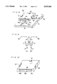
Referring to FIG. 1, the internal composition of a First embodiment is described. A couple of strip lines 2 and 3 are formed on an upper surface of a dielectric substrate 1. A lead portion 2a of the strip line 2 extends to a left end of the dielectric substrate 1, and a lead portion 2b thereof extends to a front end, in the left, of the dielectric substrate 1. A head portion 3a of the strip line 3 extends to a right end of the dielectric substrate 1, and a lead portion 3b thereof extends to a front end, in the right, of the dielectric substrate 1. On a lower surface of the dielectric substrate 1, a common ground electrode 4 is formed to cover almost the entire surface. Lead portions 4a, 4b and 4c of the ground electrode 4 extend to the front end of the dielectric substrate 1, in the left, in the center and in the right respectively. Lead portions 4d, 4e and 4f extend to a rear end of the dielectric substrate 1, in the left, in the center and in the right respectively. The strip lines 2 and 3, and the common ground electrode 4 may be formed by a printing method wherein paste of silver, copper or the like is coated and dried, or by a thin-film forming method such as spattering and photolithography. A dielectric substrate 6 is placed on the dielectric substrate 1 and joined thereto by adhesive, and thus, a strip line filter 15 is fabricated.
Referring to FIG. 2, the appearance of the strip line filter 15 is described. An input terminal electrode 7 is disposed on the left end and is in contact with the lead potion 2a of the strip line 2. An output terminal electrode 8 is disposed on the right end and is in contact with the lead portion 3a of the strip line 3. On the front end of the line strip filter 15, ground terminal electrodes 9, 10 and 11 are disposed in the left, in the center and in the right respectively. The ground terminal electrode 9 is in contact with the lead portion 2b of the strip line 2 and the lead portion 4a of the common ground electrode 4 to serve as a link therebetween. The ground terminal electrode 10 is in contact with the lead portion 4b of the common ground electrode 4 to be used for soldering. The ground terminal electrode 11 is in contact with the lead portion 3b of the strip line 3 and the lead portion 4c of the common ground electrode 4 to serve as a link therebetween. On the rear end of the line strip filter 15, ground terminal electrodes 12, 13 and 14 are disposed in the left, in the center and in the right respectively. The ground terminal electrodes 12, 13 and 14 are in contact with the lead portions 4d, 4e and 4f of the common ground electrode 4 respectively to be used for soldering. Thus, the strip lines 2 and 3 are electrically connected with the common ground electrode 4 through the link ground terminal electrodes 9 and 11 respectively. The terminal electrodes 7 through 14 may be formed by a printing method wherein paste of silver, a mixture of silver and palladium, or the like is coated and dried, or by a thin-film forming method such as spattering and photolithography. The electrodes 7 through 14 can be formed more accurately by a thin-film coating method, and in this case, when the strip line filter 15 is soldered to a printed board, the volume and the area of solder become closer to designed values.
In the first embodiment, the common ground electrode 4, which is disposed on the bottom surface of the filter 15, is coated with a material which inhibit the deposit of solder thereon. Thereby, solder used for mounting of the filter 15 will not be deposited on the common ground electrode 4. The material coated on the common ground electrode 4 is, for example, an insulating resin, ceramics or the like.
The strip line filter 15 is, for example, surface-mounted on a printed board 20 as shown in FIG. 3. As can be seen in FIG. 3, the output terminal electrode 8 and the solder ground terminal electrode 10 are electrically connected and joined to conductors 21 and 22 on the printed board 20 by solder 24 and 26. Likewise, although it is not drawn, the input terminal electrode 7 and the solder ground terminal electrodes 12, 13 and 14 are electrically connected and joined to conductors on the printed board 20 by solder.
Since the solder ground terminal electrodes 10, 12, 13 and 14 are small, it is easier to conduct the soldering such that the volume and the area of solder 26 will be designed values. In the filter 15, since the link ground terminal electrodes 9 and 11 are not soldered, current passages from the common ground electrode 4 to the strip lines 2 and 3 via the link ground terminal electrodes 9 and 11 can have designed lengths. Therefore, the strengths of residual inductances occurring on the current passages, which depend on the lengths, can be predicted during design of the filter easily, and it is possible to design a circuit of the filter, taking the residual inductances into consideration. Thus, strip line filters produced in this way do not vary very much in the strengths of residual inductances occurring on the ground terminal electrodes 9 through 14.
FIG. 4 is an equivalent electrical circuit diagram of the strip line filter 15. The strip line 2 has an inductance L1, and a capacitance C1 occurs between the strip line 2 and the common ground electrode 4. The inductance L1 and the capacitance C1 form a resonator. The strip line 3 has an inductance L2, and a capacitance C2 occurs between the strip line 3 and the common ground electrode 4. The inductance L2 and the capacitance C2 form another resonator. These resonators are electrically coupled by a mutual inductance M. L3 and L4 denote residual inductances on current passages from the common ground electrode 4 to the strip lines 2 and 3 via the link ground terminal electrodes 9 and 11 respectively. The strengths of the residual inductances L3 and L4 depend on the lengths of the current passages.
FIG. 5 shows the band-pass characteristics of the strip line filter 15. Solid lines A1 and A3 indicate the attenuation and the insertion loss of the filter 15 respectively under standard soldering conditions (soldering the filter 15 to the printed board 20 by coating an area of 1.2 mm by 1.5 mm of a conductor on the printed board 20 with solder paste by use of a mask with a thickness of 0.10 mm). A solid line A2 indicates the attenuation of the filter 15 under comparative soldering conditions (soldering the filter 15 to the printed board 20 by coating an area of 1.2 mm by 1.5 mm of a conductor on the printed board 20 with solder paste thickly by use of a mask with a thickness of 0.35 mm). Also, for comparison, the band-pass characteristics of a conventional filter which has a large ground terminal electrode are shown by dashed lines B1, B2 and B3. The dashed lines B1 and B3 indicate the attenuation and the insertion loss of the conventional filter respectively under the standard soldering conditions, and the dashed line B2 indicates the attenuation of the conventional filter under the comparative soldering conditions. Table 1 summarizes the band-pass characteristics of the filter 15 and the conventional filter which are apparent from the graph of FIG. 5. In Table 1, as for each filter, the variations of the filter characteristics between trader the standard soldering conditions and under the comparative soldering conditions are shown.
              TABLE 1                                                     
______________________________________                                    
Variation of Filter Characteristics                                       
with Difference in the Volume of Solder                                   
       Variation in                                                       
                Variation in Attenuation                                  
       Pole Positions                                                     
                (Resonance Frequency - 240 MHz)                           
______________________________________                                    
First    10-15 MHz  1.0-1.5 dB                                            
Embodiment                                                                
Prior Art                                                                 
         40-50 MHz  3.5-5.0 dB                                            
______________________________________                                    
Concerning the filter 15 of the first embodiment, the pole positions a and b, which are at both sides of the passband, move by only 10 to 15 MHz (1.0 to 1.5 dB in point of attenuation) with the difference in the volume of solder between the two different soldering conditions. On the other hand, concerning the conventional filter, the pole positions a and b move by 40 to 50 MHz (3.5 to 5.0 dB in point of attenuation) with the difference in the volume of solder between the two different soldering conditions. Thus, according to the first embodiment, the variation in the filter characteristics with a difference in the volume of solder can be inhibited to be about 30% of that of a conventional filter.
Second Embodiment: FIGS. 6 through 10
Referring to FIG. 6, the internal composition of a second embodiment is described. A couple of strip lines 32 and 33 are formed on an upper surface of a dielectric substrate 31. A lead portion 32a of the strip line 32 extends to a left end of the dielectric substrate 31, and a lead portion 32b thereof extends to a front end, in the left, of the dielectric substrate 31. A lead portion 33a of the strip line 33 extends to a right end of the dielectric substrate 31, and a lead portion 33b thereof extends to the front end, in the right, of the dielectric substrate 31. On a lower surface of the dielectric substrate 31, a common ground electrode 34 is formed to cover almost the entire surface. Lead portions 34a and 34b extend to the front end and to a rear end respectively of the dielectric substrate 31, in the center. A dielectric substrate 36 is placed on the upper surface of the dielectric substrate 31 and joined thereto by adhesive. Thus, a strip line filter 45 is fabricated.
Referring to FIG. 7, the appearance of the strip line filter 45 is described. An input terminal electrode 37 is disposed on the left end and is in contact with the lead portion 32a of the strip line 32. An output terminal electrode 38 is disposed on the right end and is in contact with the lead portion 33a of the strip line 33. A ground terminal electrode 40 is disposed on the front end. The ground terminal electrode 40 has a solder portion 40a and arm portions 40b and 40c which extend from the solder portion 40a. The width of the arm portions 40b and 40c is smaller than that of the solder portion 40a. Thereby, solder coated on the solder portion 40a will not spread to the arm portions 40b and 40c easily. The arm portion 40b is in contact with the lead portion 32b of the strip line 32. The solder portion 40a is in contact with the lead portion 34a of the common ground electrode 34. The arm portion 40c is in contact with the lead portion 33b of the strip line 33. A ground terminal electrode 43 is disposed on the rear end and is in contact with the lead portion 34b of the common ground electrode 34. Thus, the strip lines 32 and 33 are electrically connected with the common ground electrode 34 via the ground terminal electrode 40.
In the second embodiment, the common ground electrode 34, which is disposed on the bottom surface of the filter 45, is coated with a material which is difficult for solder to deposit on. Thereby, solder used for mounting of the filter 45 will not be deposited on the common ground electrode 34.
The strip line filter 45 is, for example, surface-mounted on a printed board 50 as shown in FIG. 8. More specifically, as can be seen in FIG. 8, the output terminal electrode 38 and the ground terminal electrode 40 are electrically connected and joined to conductors 51 and 52 on the surface of the printed board 50 by solder 54 and 56. At that time, the solder 56 is deposited on the solder portion 40a of the ground terminal electrode 40 but is not deposited on the arm portions 40b and 40c. Likewise, although it is not drawn, the input terminal electrode 37 and the ground terminal electrode 43 are electrically connected and joined to conductors on the surface of the printed board 50 by solder.
Since the solder portion 40a of the ground terminal electrode 40 is small, it is easier to conduct the soldering such that the volume and the area of solder 26 will be designed values. Since the arm portions 40b and 40c of the ground terminal electrode 40 are not soldered, current passages from the common ground electrode 34 to the strip lines 32 and 33 via the ground terminal electrode 40 can have designed lengths. Therefore, the strengths of residual inductances occurring on the current passages, which depend on the lengths, can be predicted during design of the filter easily, and it is possible to design a circuit of the filter, taking the residual inductances into consideration. Thus, strip line filters produced in tills way do not vary very much in the strengths of residual inductances occurring on the ground terminal electrode 40.
FIG. 9 is an equivalent electrical circuit diagram of the strip line filter 45. The strip line 32 has an inductance L1, and a capacitance C1 occurs between the strip line 32 and the common ground electrode 34. The inductance L1 and the capacitance C1 form a resonator. The strip line 33 has an inductance L2, and a capacitance C2 occurs between the strip line 33 and the common ground electrode 34. The inductance L2 and the capacitance C2 form another resonator. These resonators are electrically coupled by a mutual inductance M. L3 and L4 denote residual inductances occurring on current passages from the common ground electrode 34 to the strip lines 32 and 33 via the ground terminal electrode 40. The strengths of the residual inductances L3 and L4 depend on the lengths of the current passages.
Table 2 shows variation In the band-pass characteristics of the strip line filter 45 between under standard soldering conditions and under comparative soldering conditions. The standard soldering conditions and the comparative soldering conditions are those described in connection with the first embodiment. Also, for comparison, variation in the band-pass characteristics of a conventional filter which has a large ground terminal electrode is shown. Values in Table 2 were obtained from a graph like the graph of FIG. 5.
              TABLE 2                                                     
______________________________________                                    
Variation of Filter Characteristics                                       
with Difference in the Volume of Solder                                   
       Variation in                                                       
                Variation in Attenuation                                  
       Pole Positions                                                     
                (Resonance Frequency - 240 MHz)                           
______________________________________                                    
Second   15-20 MHz  1.5-2.5 dB                                            
Embodiment                                                                
Prior Art                                                                 
         40-50 MHz  3.5-5.0 dB                                            
______________________________________                                    
Concerning the filter 45 of the second embodiment, the pole positions a and b, which are at both sides of the passband, move by only 15 to 20 MHz (1.5 to 2.5 dB in point of attenuation) with the difference in the volume of solder between the two different conditions. Concerning the conventional filter, on the other hand, the pole positions a and b move by 40 to 50 MHz (3.5 to 5.0 dB in point of attenuation). Thus, according to the second embodiment, the variation in the filter characteristics with a difference in the volume of solder can be inhibited to be about 40% of that of a conventional filter.
The ground terminal electrode with the arm portions may be of any configuration in accordance with the specification of the strip line filter. For example, as shown in FIG. 10, the ground terminal electrode can be made to be T-shaped 48, formed of a solder portions 48a and arm portions 48b and 48c.
Third Embodiment: FIGS. 11 and 12
Referring to FIG. 11, the internal composition of a strip line filter 61 of a third embodiment is described. A dielectric green sheet 62 which has strip lines 65 and 66 on a surface, a dielectric green sheet 63 which has a common ground electrode 67 on a surface and a dielectric green sheet 64 are laminated. The laminated green sheets are pressed and sintered to be a unified body.
A lead portion 65a of the strip line 65 extends to a left end of the dielectric green sheet 62, and a lead portion 65b thereof extends to a front end, in the left, of the dielectric green sheet 62. A lead portion 66a of the strip line 66 extends to a right end of the dielectric green sheet 62, and a lead portion 66b thereof extends to the front end, in the right of the dielectric green sheet 62. Lead portions 67a, 67b and 67c of the common ground electrode 67 extend to the front end of the dielectric green sheet 63, in the left, in the center and in the right respectively. Further, lead portions 67d, 67e and 67f of the common ground electrode 67 extend to a rear end of the dielectric green sheet 63, in the left, in the center and in the right respectively.
Referring to FIG. 12, the appearance of the strip line filter 61 is described. An input terminal electrode 69 is disposed on the left end of the strip line filter 61 and is in contact with the lead portion 65a of the strip line 65. An output terminal electrode 70 is disposed on the right end and is in contact with the lead portions 66a of the strip line 66. A ground terminal electrode 71 is disposed on the front end, in the left, of the strip line filter 61. The ground terminal electrode 71 is in contact with the lead portion 65b of the strip line 65 and the lead portion 67a of the common ground electrode 67 and serves as a link therebetween. A ground terminal electrode 72 is disposed on the front end, in the center, of the strip line filter 61. The ground terminal electrode 72 is in contact with the lead portions 67b of the common ground electrode 67 and is used for soldering. A ground terminal electrode 73 is disposed on the front end, in the right, of the strip line filter 61. The ground terminal electrode 73 is in contact with the lead portion 66b of the strip line 66 and the lead portion 67c of the common ground terminal 67 and serves as a link therebetween. Ground terminal electrodes 74, 75 and 76 are disposed on the rear end, in the left, in the center and in the right, of the strip line filter 61. The ground terminal electrodes 74, 75 and 76 are in contact with the lead portions 67d, 67e and 67f of the common ground electrode 67 respectively and are used for soldering. Thus, the strip lines 65 and 66 are electrically connected with the common ground electrode 67 via the link ground terminal electrodes 71 and 73 respectively.
The strip line filter 61 has the same action and the same effect as the filter 15 of the first embodiment does.
Fourth Embodiment: FIG. 13
FIG. 13 shows a strip line filter 81 of a fourth embodiment. Like the strip line filter 61 off the third embodiment, the strip line filter 81 comprises the dielectric green sheet 62 with the strip lines 65 and 66, the dielectric green sheet 63 with the common ground electrode 67, and the dielectric green sheet 64. The dielectric green sheets 62, 63 and 64 are laminated, and the laminated green sheets are pressed and sintered to be a unified body. Description of the configurations of the strip lines 65 and 66 and the common ground electrode 67 is omitted.
An input terminal electrode 82 is disposed on the left end of the strip line filter 81 and is in contact with the lead portion 65a of the strip line 65. An output terminal electrode 83 is disposed on the right end of the strip line filter 81 and is in contact with the lead portion 66a of the strip line 66. A ground terminal electrode 84 is disposed on the front end of the strip Line filter 81. The ground terminal electrode 84 has a solder portion 84a, and arm portions 84b and 84c which extend from the solder portion 84a. The arm portion 84b is in contact with the lead portion 65b of the strip line 65 and the lead portion 67a of the common ground electrode 67. The solder portion 84a is in contact with the lead portion 67b of the common ground electrode 67. The arm portion 84c is in contact with the lead portion 66b of the strip line 66 and the lead portion 67c of the common ground electrode 67. Further, ground terminal electrodes 85, 86 and 87 are disposed on the rear end of the strip line filter 81, in the left, in the center and in the right, and are in contact with the lead portions 67d, 67e and 67f of the common ground electrode 67 respectively. Thus, the strip lines 65 and 66 are electrically connected with the common ground electrode 67 via the ground terminal electrode 84.
The strip line filter 81 has the same action and the same effect as the filter 45 of the second embodiment does.
Other Embodiments
In order to certainly prevent deposition of solder on the link ground terminal electrodes, the link ground terminal electrodes may be coated with a material which is difficult for solder to deposit on, such as an insulating resin. Likewise, the arm portions of the ground terminal electrode may be coated with a material which is difficult for solder to deposit on.
The number of solder ground terminal electrodes disposed on one end of a filter may be two or more, and the number of link ground terminal electrodes may be three or more.
In the above embodiments, one or more dielectric substrates having electrodes thereon and a dielectric substrate with no electrodes are bonded by adhesive. There are other processes adoptable for manufacture of the filters. For example, the filters may be manufactured by the following process: first, electrodes are formed on ceramic dielectric green sheets by printing of paste; then, the ceramic dielectric green sheets with electrodes are laminated; and the laminated green sheets are sintered to be unified into a body.
Although the present invention has been described in connection with the preferred embodiments above, it is to be noted that various changes and modifications are possible to those who are skilled in the art. Such changes and modifications are to be understood as being within the scope of the present invention.

Claims (25)

What is claimed is:
1. A strip line filter comprising:
a dielectric substrate having a first surface and a second surface;
at least two strip lines provided on the first surface of the substrate;
a common ground electrode provided on the second surface of the substrate;
a solder ground terminal electrode provided on an end of the substrate, the solder ground terminal electrode being electrically connected with the common ground electrode, and with no electrical connection to the strip lines and soldered to a conductor on a circuit board;
at least two link ground terminal electrodes provided on the end of the substrate at a distance from the solder ground terminal electrode, the link ground terminal electrodes electrically connecting each of the strip lines with the common ground electrode and not soldered to any conductors on the circuit board;
an input terminal electrode provided on the substrate, the input terminal electrode being electrically connected with one of the strip lines; and
an output terminal electrode provided on the substrate, the output terminal electrode being electrically connected with another of the strip lines;
wherein the link ground terminal electrodes are coated with a material which inhibits the deposit of solder thereon.
2. A strip line filter as claimed in claim 1, wherein the substrate, the strip lines and the common ground electrode form at least two resonators.
3. A strip line filter as claimed in claim 1, further comprising a dielectric substrate which is laid on the first surface of the substrate.
4. A strip line filter comprising:
a dielectric substrate having a first surface and a second surface;
at least two strip lines provided on the first surface of the substrate;
a common ground electrode provided on the second surface of the substrate;
a solder ground terminal electrode provided on an end of the substrate, the solder ground terminal electrode being electrically connected with the common ground electrode, and with no electrical connection to the strip lines and soldered to a conductor on a circuit board;
at least two link ground terminal electrodes provided on the end of the substrate at a distance from the solder ground terminal electrode, the link ground terminal electrodes electrically connecting each of the strip lines with the common ground electrode and not soldered to any conductors on the circuit board;
an input terminal electrode provided on the substrate, the input terminal electrode being electrically connected with one of the strip lines; and
an output terminal electrode provided on the substrate, the output terminal electrode being electrically connected with another of the strip lines;
wherein the common ground electrode is coated with a material which inhibits the deposit of solder thereon.
5. A strip line filter as claimed in claim 4, wherein the first and second substrates, the strip lines and the common ground electrode form at least two resonators.
6. A strip line filter comprising:
a first dielectric substrate with at least two strip lines on a surface;
a second dielectric substrate with a common ground electrode on a surface;
a solder ground terminal electrode provided on an end of a laminate of the first substrate and the second substrate, the solder ground terminal electrode being electrically connected with the common ground electrode, and with no electrical connection to the strip lines and soldered to a conductor on a circuit board;
at least two link ground terminal electrodes provided on the end of the laminate at a distance from the solder ground terminal electrode, the link ground terminal electrodes electrically connecting each of the strip lines with the common ground electrode, and not soldered to any conductor on the circuit board;
an input terminal electrode provided on the laminate, the input terminal electrode being electrically connected with one of the strip lines; and
an output terminal electrode provided on the laminate, the output terminal electrode being electrically connected with another of the strip lines;
wherein the link ground terminal electrodes are coated with a material which inhibits the deposit of solder thereon.
7. A strip line filter as claimed in claim 6, further comprising a dielectric substrate which is laid on the surface of the first substrate.
8. A strip line filter comprising:
a dielectric substrate having a first surface and a second surface;
at least two strip lines provided on the first surface of the substrate;
a common ground electrode provided on the second surface of the substrate;
a ground terminal electrode provided on an end of the substrate, the ground terminal electrode having a solder portion and at least two arm portions which extend from the solder portion, the ground terminal electrode being electrically connected with the common ground electrode via the solder portion and with the strip lines via the arm portions;
an input terminal electrode provided on the substrate, the input terminal electrode being electrically connected with one of the strip lines; and
an output terminal electrode provided on the substrate, the output terminal electrode being electrically connected with another of the strip lines.
9. A strip line filter as claimed in claim 8, wherein the substrate, the strip lines and the common ground electrode form at least two resonators.
10. A strip line filter as claimed in claim 8, wherein the arm portions of the ground terminal electrode are coated with a material which inhibits the deposit of solder thereon.
11. A strip line filter as claimed in claim 8, further comprising a dielectric substrate which is laid on the first surface of the substrate.
12. A strip line filter as claimed in claim 8, wherein the common ground electrode is coated with a material which inhibits the deposit of solder thereon.
13. A strip line filter, comprising:
a first dielectric substrate with at least two strip lines on a surface;
a second dielectric substrate with a common ground electrode on a surface;
a ground terminal electrode provided on an end of a laminate of the first substrate and the second substrate, the ground terminal electrode having a solder portion and at least two arm portions which extend from the solder portion, the ground terminal electrode being electrically connected with the common ground electrode via the solder portion and with the strip lines via the arm portions;
an input terminal electrode provided on the laminate, the input terminal electrode being electrically connected with one of the strip lines; and
an output terminal electrode provided on the laminate, the output terminal electrode being electrically connected with another of the strip lines.
14. A strip line filter as claimed in claim 13, wherein the first and second substrates, the strip lines and the common ground electrode form at least two resonators.
15. A strip line filter as claimed in claim 13, wherein the arm portions of the ground terminal electrode are coated with a material which inhibits the deposit of solder thereon.
16. A strip line filter as claimed in claim 13, further comprising a dielectric substrate which is laid on the first surface of the substrate.
17. A combination of a strip line filter and a circuit board, comprising:
a circuit board which has a plurality of conductors thereon:
a dielectric substrate having a first surface and a second surface;
at least two strip lines provided on the first surface of the substrate;
a common ground electrode provided on the second surface of the substrate;
a solder ground terminal electrode provided on an end of the substrate, the solder ground terminal electrode being electrically connected with the common ground electrode, and with no electrical connection to the strip lines;
at least two link ground terminal electrodes provided on the end of the substrate at a distance from the solder ground terminal electrode, the link ground terminal electrodes electrically connecting each of the strip lines with the common ground electrode;
an input terminal electrode provided on the substrate, the input terminal electrode being electrically connected with one of the strip lines; and
an output terminal electrode provided on the substrate, the output terminal electrode being electrically connected with another of the strip lines;
wherein, the solder ground terminal electrode, the input terminal electrode and the output terminal electrode are soldered to separate conductors of the circuit board, and the link ground terminal electrodes are not soldered to any conductors of the circuit board.
18. A combination of a strip line filter and a circuit board as claimed in claim 17, wherein the substrate, the strip lines and the common ground electrode form at least two resonators.
19. A combination of a strip line filter and a circuit board as claimed in claim 17, wherein the link ground terminal electrodes are coated with a material which inhibits the deposit of solder thereon.
20. A combination of a strip line filter and a circuit board as claimed in claim 17, wherein the common ground electrode is coated with a material which inhibits the deposit of solder thereon.
21. A combination of a strip line filter and a circuit board, comprising:
a circuit board which has a plurality of conductors thereon;
a first dielectric substrate with at least two strip lines on a surface;
a second dielectric substrate with a common ground electrode on a surface;
a solder ground terminal electrode provided on an end of a laminate of the first substrate and the second substrate, the solder ground terminal electrode being electrically connected with the common ground electrode, and with no electrical connection to the strip lines:
at least two link ground terminal electrodes provided on the end of the laminate at a distance from the solder ground terminal electrode, the link ground terminal electrodes electrically connecting each of the strip lines with the common ground electrode;
an input terminal electrode provided on the laminate, the input terminal electrode being electrically connected with one of the strip lines; and
an output terminal electrode provided on the laminate, the output terminal electrode being electrically connected with another of the strip lines;
wherein, the solder ground terminal electrode, the input terminal electrode and the output terminal electrode are soldered to separate conductors of the circuit board, and the link ground terminal electrodes are not soldered to any conductors of the circuit board.
22. A combination of a strip line filter and a circuit board as claimed in claim 21, wherein the first and second substrate, the strip lines and the common ground electrode form at least two resonators.
23. A combination of a strip line filter and a circuit board as claimed in claim 21, wherein the link ground terminal electrodes are coated with a material which inhibits the deposit of solder thereon.
24. A strip line filter as claimed in claim 4, wherein the substrate, the strip lines and the common ground electrode form at least two resonators.
25. A strip line filter as claimed in claim 4, further comprising a dielectric substrate which is laid on the first surface of the substrate.
US08/252,238 1993-06-08 1994-06-01 Strip line filter Expired - Lifetime US5519366A (en)

Applications Claiming Priority (4)

Application Number Priority Date Filing Date Title
JP5-137648 1993-06-08
JP5-137647 1993-06-08
JP13764893A JP2869913B2 (en) 1993-06-08 1993-06-08 Stripline filter
JP13764793A JP2869912B2 (en) 1993-06-08 1993-06-08 Stripline filter

Publications (1)

Publication Number Publication Date
US5519366A true US5519366A (en) 1996-05-21

Family

ID=26470886

Family Applications (1)

Application Number Title Priority Date Filing Date
US08/252,238 Expired - Lifetime US5519366A (en) 1993-06-08 1994-06-01 Strip line filter

Country Status (3)

Country Link
US (1) US5519366A (en)
KR (1) KR0150253B1 (en)
DE (1) DE4420060C2 (en)

Cited By (11)

* Cited by examiner, † Cited by third party
Publication number Priority date Publication date Assignee Title
US5770986A (en) * 1994-06-14 1998-06-23 Murata Manufacturing Co., Ltd. Stripline filter with a stripline-formed parallel capacitor
US6597259B1 (en) * 2000-01-11 2003-07-22 James Michael Peters Selective laminated filter structures and antenna duplexer using same
US20040172607A1 (en) * 2003-02-28 2004-09-02 Tiberiu Jamneala Method of characterizing an electronic device having unbalanced ground currents
US20050104691A1 (en) * 2003-11-14 2005-05-19 Doron Gamliel Isolation of miniature filters
US20060276343A1 (en) * 2002-12-20 2006-12-07 Bisong Cao Superconductive microstrip resonator and filter
WO2007056864A1 (en) 2005-11-21 2007-05-24 Kenneth Kam-Sing Ho Underwater camera combination
US20080246157A1 (en) * 2007-04-03 2008-10-09 Qiang Richard Chen Surface mount devices with minimum lead inductance and methods of manufacturing the same
US20100013577A1 (en) * 2007-03-27 2010-01-21 Kyocera Corporation Bandpass filter, wireless communication module and wireless communication device
US20100090783A1 (en) * 2008-10-15 2010-04-15 Murata Manufacturing Co., Ltd. Strip line filter
US20100265012A1 (en) * 2007-12-19 2010-10-21 Murata Manufacturing Co., Ltd. Stripline Filter and Manufacturing Method Thereof
US20120062344A1 (en) * 2009-05-26 2012-03-15 Murata Manufacturing Co., Ltd. Stripline Filter

Families Citing this family (2)

* Cited by examiner, † Cited by third party
Publication number Priority date Publication date Assignee Title
KR100806389B1 (en) * 2006-01-09 2008-02-27 삼성전자주식회사 Parallel coupled cpw line filter
JP6839692B2 (en) * 2018-10-19 2021-03-10 双信電機株式会社 filter

Citations (2)

* Cited by examiner, † Cited by third party
Publication number Priority date Publication date Assignee Title
US5351020A (en) * 1991-02-15 1994-09-27 Myrata Manufacturing Co., Ltd. Band-pass filter having three or more loop-shaped electrodes
US5357227A (en) * 1992-04-16 1994-10-18 Murata Mfg. Co., Ltd. Laminated high-frequency low-pass filter

Family Cites Families (1)

* Cited by examiner, † Cited by third party
Publication number Priority date Publication date Assignee Title
JPH03196701A (en) * 1989-08-25 1991-08-28 Ngk Spark Plug Co Ltd Frequency adjustment method for three-conductor structure filter

Patent Citations (2)

* Cited by examiner, † Cited by third party
Publication number Priority date Publication date Assignee Title
US5351020A (en) * 1991-02-15 1994-09-27 Myrata Manufacturing Co., Ltd. Band-pass filter having three or more loop-shaped electrodes
US5357227A (en) * 1992-04-16 1994-10-18 Murata Mfg. Co., Ltd. Laminated high-frequency low-pass filter

Cited By (20)

* Cited by examiner, † Cited by third party
Publication number Priority date Publication date Assignee Title
US5770986A (en) * 1994-06-14 1998-06-23 Murata Manufacturing Co., Ltd. Stripline filter with a stripline-formed parallel capacitor
US6597259B1 (en) * 2000-01-11 2003-07-22 James Michael Peters Selective laminated filter structures and antenna duplexer using same
US20060276343A1 (en) * 2002-12-20 2006-12-07 Bisong Cao Superconductive microstrip resonator and filter
US7532918B2 (en) * 2002-12-20 2009-05-12 Tsinghua University Superconductive filter having U-type microstrip resonators with longer and shorter parallel sides
US20040172607A1 (en) * 2003-02-28 2004-09-02 Tiberiu Jamneala Method of characterizing an electronic device having unbalanced ground currents
US6804807B2 (en) * 2003-02-28 2004-10-12 Agilent Technologies, Inc. Method of characterizing an electronic device having unbalanced ground currents
US6943646B2 (en) * 2003-11-14 2005-09-13 Doron Gamliel Isolation of miniature filters
US20050104691A1 (en) * 2003-11-14 2005-05-19 Doron Gamliel Isolation of miniature filters
WO2007056864A1 (en) 2005-11-21 2007-05-24 Kenneth Kam-Sing Ho Underwater camera combination
US20100013577A1 (en) * 2007-03-27 2010-01-21 Kyocera Corporation Bandpass filter, wireless communication module and wireless communication device
US8493163B2 (en) * 2007-03-27 2013-07-23 Kyocera Corporation Bandpass filter, wireless communication module and wireless communication device
US8493744B2 (en) 2007-04-03 2013-07-23 Tdk Corporation Surface mount devices with minimum lead inductance and methods of manufacturing the same
US20080246157A1 (en) * 2007-04-03 2008-10-09 Qiang Richard Chen Surface mount devices with minimum lead inductance and methods of manufacturing the same
WO2008124259A1 (en) * 2007-04-03 2008-10-16 Tdk Corporation Surface mount devices with minimum lead inductance and methods of manufacturing the same
US20100265012A1 (en) * 2007-12-19 2010-10-21 Murata Manufacturing Co., Ltd. Stripline Filter and Manufacturing Method Thereof
US8008995B2 (en) * 2007-12-19 2011-08-30 Murata Manufacturing Co., Ltd. Stripline filter and manufacturing method thereof
US8203401B2 (en) * 2008-10-15 2012-06-19 Murata Manufacturing Co., Ltd. Strip line filter
US20100090783A1 (en) * 2008-10-15 2010-04-15 Murata Manufacturing Co., Ltd. Strip line filter
US20120062344A1 (en) * 2009-05-26 2012-03-15 Murata Manufacturing Co., Ltd. Stripline Filter
US8686811B2 (en) * 2009-05-26 2014-04-01 Murata Manufacturing Co., Ltd. Stripline filter

Also Published As

Publication number Publication date
DE4420060A1 (en) 1994-12-15
KR950002104A (en) 1995-01-04
DE4420060C2 (en) 1997-05-22
KR0150253B1 (en) 1998-11-02

Similar Documents

Publication Publication Date Title
US5396201A (en) Dielectric filter having inter-resonator coupling including both magnetic and electric coupling
US4673902A (en) Dielectric material coaxial resonator filter directly mountable on a circuit board
US6529102B2 (en) LC filter circuit and laminated type LC filter
US5519366A (en) Strip line filter
US6714100B2 (en) Monolithic electronic device
JPH0491501A (en) Dielectric filter
US5196813A (en) Dielectric filter having a single multilayer substrate
JP2002280864A (en) Power bisecting circuit and power bisecting component
JP2843722B2 (en) Laminated LC chip component and manufacturing method thereof
JP2661004B2 (en) Dielectric filter
JP2906828B2 (en) Surface mount type dielectric filter
JP2869913B2 (en) Stripline filter
JPH06125202A (en) Dielectric filter and its pass band width control method
JP2869912B2 (en) Stripline filter
JPH07202522A (en) Mounting structure for electronic parts
JP2611718B2 (en) Semiconductor device
JPS584164Y2 (en) variable resistance attenuator
JP3017917B2 (en) Dielectric resonator
KR100213374B1 (en) Small dielectric filter
JPH05243807A (en) Dielectric filter
JPH0846403A (en) Substrate for dielectric filter and dielectric filter
JPH04356801A (en) Dielectric filter
JPH07283612A (en) Dielectric filter
JPH04123604U (en) dielectric filter
JPH06125204A (en) Dielectric filter

Legal Events

Date Code Title Description
AS Assignment

Owner name: MURATA MANUFACTURING CO., LTD., A CORP. OF JAPAN,

Free format text: ASSIGNMENT OF ASSIGNORS INTEREST;ASSIGNORS:KANEKO, TOSHIMI;KAWAGUCHI, MASAHIKO;MATSUTA, KATSUJI;REEL/FRAME:007018/0975

Effective date: 19940526

FEPP Fee payment procedure

Free format text: PAYOR NUMBER ASSIGNED (ORIGINAL EVENT CODE: ASPN); ENTITY STATUS OF PATENT OWNER: LARGE ENTITY

STCF Information on status: patent grant

Free format text: PATENTED CASE

FP Lapsed due to failure to pay maintenance fee

Effective date: 19961030

FPAY Fee payment

Year of fee payment: 4

FPAY Fee payment

Year of fee payment: 8

FPAY Fee payment

Year of fee payment: 12