EP0535350B1 - Verfahren zur Herstellung eines seitlich begrenzten, einkristallinen Gebietes in einem Bipolartransistor - Google Patents
Verfahren zur Herstellung eines seitlich begrenzten, einkristallinen Gebietes in einem Bipolartransistor Download PDFInfo
- Publication number
- EP0535350B1 EP0535350B1 EP92114161A EP92114161A EP0535350B1 EP 0535350 B1 EP0535350 B1 EP 0535350B1 EP 92114161 A EP92114161 A EP 92114161A EP 92114161 A EP92114161 A EP 92114161A EP 0535350 B1 EP0535350 B1 EP 0535350B1
- Authority
- EP
- European Patent Office
- Prior art keywords
- layer
- region
- substrate
- silicon
- respect
- Prior art date
- Legal status (The legal status is an assumption and is not a legal conclusion. Google has not performed a legal analysis and makes no representation as to the accuracy of the status listed.)
- Expired - Lifetime
Links
Images


Classifications
-
- H—ELECTRICITY
- H10—SEMICONDUCTOR DEVICES; ELECTRIC SOLID-STATE DEVICES NOT OTHERWISE PROVIDED FOR
- H10D—INORGANIC ELECTRIC SEMICONDUCTOR DEVICES
- H10D10/00—Bipolar junction transistors [BJT]
- H10D10/01—Manufacture or treatment
- H10D10/051—Manufacture or treatment of vertical BJTs
- H10D10/054—Forming extrinsic base regions on silicon substrate after insulating device isolation in vertical BJTs having single crystalline emitter, collector or base regions
-
- H—ELECTRICITY
- H10—SEMICONDUCTOR DEVICES; ELECTRIC SOLID-STATE DEVICES NOT OTHERWISE PROVIDED FOR
- H10D—INORGANIC ELECTRIC SEMICONDUCTOR DEVICES
- H10D30/00—Field-effect transistors [FET]
- H10D30/01—Manufacture or treatment
- H10D30/021—Manufacture or treatment of FETs having insulated gates [IGFET]
- H10D30/027—Manufacture or treatment of FETs having insulated gates [IGFET] of lateral single-gate IGFETs
- H10D30/0278—Manufacture or treatment of FETs having insulated gates [IGFET] of lateral single-gate IGFETs forming single crystalline channels on wafers after forming insulating device isolations
-
- H—ELECTRICITY
- H10—SEMICONDUCTOR DEVICES; ELECTRIC SOLID-STATE DEVICES NOT OTHERWISE PROVIDED FOR
- H10P—GENERIC PROCESSES OR APPARATUS FOR THE MANUFACTURE OR TREATMENT OF DEVICES COVERED BY CLASS H10
- H10P14/00—Formation of materials, e.g. in the shape of layers or pillars
- H10P14/20—Formation of materials, e.g. in the shape of layers or pillars of semiconductor materials
- H10P14/27—Formation of materials, e.g. in the shape of layers or pillars of semiconductor materials using selective deposition, e.g. simultaneous growth of monocrystalline and non-monocrystalline semiconductor materials
- H10P14/271—Formation of materials, e.g. in the shape of layers or pillars of semiconductor materials using selective deposition, e.g. simultaneous growth of monocrystalline and non-monocrystalline semiconductor materials characterised by the preparation of substrate for selective deposition
-
- H—ELECTRICITY
- H10—SEMICONDUCTOR DEVICES; ELECTRIC SOLID-STATE DEVICES NOT OTHERWISE PROVIDED FOR
- H10P—GENERIC PROCESSES OR APPARATUS FOR THE MANUFACTURE OR TREATMENT OF DEVICES COVERED BY CLASS H10
- H10P14/00—Formation of materials, e.g. in the shape of layers or pillars
- H10P14/20—Formation of materials, e.g. in the shape of layers or pillars of semiconductor materials
- H10P14/29—Formation of materials, e.g. in the shape of layers or pillars of semiconductor materials characterised by the substrates
- H10P14/2901—Materials
- H10P14/2902—Materials being Group IVA materials
- H10P14/2905—Silicon, silicon germanium or germanium
-
- H—ELECTRICITY
- H10—SEMICONDUCTOR DEVICES; ELECTRIC SOLID-STATE DEVICES NOT OTHERWISE PROVIDED FOR
- H10P—GENERIC PROCESSES OR APPARATUS FOR THE MANUFACTURE OR TREATMENT OF DEVICES COVERED BY CLASS H10
- H10P14/00—Formation of materials, e.g. in the shape of layers or pillars
- H10P14/20—Formation of materials, e.g. in the shape of layers or pillars of semiconductor materials
- H10P14/32—Formation of materials, e.g. in the shape of layers or pillars of semiconductor materials characterised by intermediate layers between substrates and deposited layers
- H10P14/3202—Materials thereof
- H10P14/3204—Materials thereof being Group IVA semiconducting materials
- H10P14/3211—Silicon, silicon germanium or germanium
-
- H—ELECTRICITY
- H10—SEMICONDUCTOR DEVICES; ELECTRIC SOLID-STATE DEVICES NOT OTHERWISE PROVIDED FOR
- H10P—GENERIC PROCESSES OR APPARATUS FOR THE MANUFACTURE OR TREATMENT OF DEVICES COVERED BY CLASS H10
- H10P14/00—Formation of materials, e.g. in the shape of layers or pillars
- H10P14/20—Formation of materials, e.g. in the shape of layers or pillars of semiconductor materials
- H10P14/32—Formation of materials, e.g. in the shape of layers or pillars of semiconductor materials characterised by intermediate layers between substrates and deposited layers
- H10P14/3202—Materials thereof
- H10P14/3238—Materials thereof being insulating materials
-
- H—ELECTRICITY
- H10—SEMICONDUCTOR DEVICES; ELECTRIC SOLID-STATE DEVICES NOT OTHERWISE PROVIDED FOR
- H10P—GENERIC PROCESSES OR APPARATUS FOR THE MANUFACTURE OR TREATMENT OF DEVICES COVERED BY CLASS H10
- H10P14/00—Formation of materials, e.g. in the shape of layers or pillars
- H10P14/20—Formation of materials, e.g. in the shape of layers or pillars of semiconductor materials
- H10P14/32—Formation of materials, e.g. in the shape of layers or pillars of semiconductor materials characterised by intermediate layers between substrates and deposited layers
- H10P14/3242—Structure
- H10P14/3244—Layer structure
- H10P14/3251—Layer structure consisting of three or more layers
-
- H—ELECTRICITY
- H10—SEMICONDUCTOR DEVICES; ELECTRIC SOLID-STATE DEVICES NOT OTHERWISE PROVIDED FOR
- H10P—GENERIC PROCESSES OR APPARATUS FOR THE MANUFACTURE OR TREATMENT OF DEVICES COVERED BY CLASS H10
- H10P14/00—Formation of materials, e.g. in the shape of layers or pillars
- H10P14/20—Formation of materials, e.g. in the shape of layers or pillars of semiconductor materials
- H10P14/34—Deposited materials, e.g. layers
- H10P14/3402—Deposited materials, e.g. layers characterised by the chemical composition
- H10P14/3404—Deposited materials, e.g. layers characterised by the chemical composition being Group IVA materials
- H10P14/3411—Silicon, silicon germanium or germanium
-
- Y—GENERAL TAGGING OF NEW TECHNOLOGICAL DEVELOPMENTS; GENERAL TAGGING OF CROSS-SECTIONAL TECHNOLOGIES SPANNING OVER SEVERAL SECTIONS OF THE IPC; TECHNICAL SUBJECTS COVERED BY FORMER USPC CROSS-REFERENCE ART COLLECTIONS [XRACs] AND DIGESTS
- Y10—TECHNICAL SUBJECTS COVERED BY FORMER USPC
- Y10S—TECHNICAL SUBJECTS COVERED BY FORMER USPC CROSS-REFERENCE ART COLLECTIONS [XRACs] AND DIGESTS
- Y10S148/00—Metal treatment
- Y10S148/011—Bipolar transistors
Definitions
- From US-A-5 028 557 is a simultaneous method Manufacture of bipolar and field effect transistors known.
- a monocrystalline semiconductor substrate is used doped polycrystalline silicon layer applied.
- the Polysilicon layer is of the opposite conductivity type as the Subsrat endowed. Then openings in the polysilicon layer with essentially vertical flanks formed the surface of the substrate in the areas expose in which an emitter or a gate is formed becomes.
- the structure becomes Polysilicon layer driven out dopant and in the substrate doped areas for the base of the bipolar transistors or Source / drain regions of the field effect transistors are formed.
- EP-AO 042 698 discloses a semiconductor arrangement in which doped polysilicon layers which have been used to form doped regions during the production of a diffusion source are used as electrodes.
- an SiO 2 layer and an Si 3 N 4 layer are deposited over it.
- the SiO 2 layer is structured so that the surface of the substrate is exposed in the area of the contact.
- the SiO 2 layer is also etched back under the Si 3 N 4 layer.
- polysilicon is also deposited on the flanks of the Si 3 N 4 layer.
- the invention is based on the problem of a method for Manufacture of a bipolar transistor specifying a side limited, single-crystal area as an active part and the one deep collector connection for contacting of the collector to the side of the single crystal area having.
- the single-crystal region grows up the surface of the substrate on the side through the structured first layer is limited. Because the first Layer has an undercut under the second layer, are those parts of the single-crystalline region in which Crystal defects or grain boundaries occur below the Edges of the second layer. Within the structured second layer is the single-crystal region thus produced essentially free of crystal defects and meets the requirements for use as an active part of a Transistor.
- the single crystal area by adding dopant-containing compounds in the to dope selective epitaxy in situ. That has the advantage, that the single crystalline area with a perpendicular to the surface of the substrate-running dopant profile can be produced is. It is particularly possible that the single crystal area to dope on the surface of a conductivity type and underneath a thin layer of the opposite conductivity type to provide.
- a silicon substrate is used.
- the single-crystalline region thereon is generally produced from the same semiconductor material, ie also from silicon.
- another semiconductor material e.g. B. germanium, so that the single-crystalline region consists of Si 1-x Ge x where x is between 0.2 and 0.4. In this way, the method is suitable for the production of hetero components.
- the first layer made of SiO 2 and the second layer made of polycrystalline silicon are covered with a third layer before the generation of the undercuts, on the surface of which no nucleation takes place during the selective epitaxy and which resists the etching of the second layer and the first layer.
- Si 3 N 4 is particularly suitable for this.
- the third layer of Si 3 N 4 can remain on the second layer of polycrystalline silicon after the selective epitaxy. However, it is advantageous to remove them since this avoids tension in the finished component.
- the second layer of polycrystalline Silicon By doping the second layer of polycrystalline Silicon is the second layer as a connection for the single crystal Area usable. In this way, self-adjustment is carried out a terminal is formed to the single crystal region.
- the inventive method for producing a single-crystalline Area is suitable in producing a Bipolar transistor to be applied.
- a Bipolar transistor to be applied.
- the substrate below the single crystal region
- Collector formed.
- a Base formed.
- z. B. the single crystal region even the base.
- the single crystal area is a continuation of the collector represents, in which the base is formed by implantation.
- An emitter is formed above the base, e.g. B. by Deposition of an appropriately doped polycrystalline Silicon layer and subsequent diffusion.
- the second Layer of polycrystalline silicon is doped and structured so that it forms a basic connection. In this The bipolar transistor is self-aligned for the base connection Base arranged.
- the collector is connected by a collector connection located on the side of the emitter and base.
- a collector connection located on the side of the emitter and base.
- the fourth layer is planarized so that the surface of the second layer is exposed.
- a mask is generated which defines a first area for the emitter, base and collector and laterally a second area for a collector connection.
- an anisotropic etching step that is selective with respect to silicon, the surface of the second layer is exposed in the first region and the surface of the substrate in the second region.
- the second layer of polycrystalline silicon in the first area and the surface of the substrate in the second area act as an etch stop.
- the second layer is removed in the first region and an etching trench is produced in the surface of the substrate in the second region.
- the depth of the etching trench is controlled over the duration of the etching step.
- the first region and the second region are formed simultaneously using the same etching steps.
- the exposed flanks of all layers adjacent to the first region and the second region are covered with the third layer of, for. B. Si 3 N 4 covered.
- flank coverings spacers
- the exposed oxide layer is removed selectively to the silicon by wet chemical means.
- the flank coverings serve for insulation between the second layer forming the base connection and the emitter connection to be subsequently produced. Furthermore, the active part of the single-crystalline region is defined by the flank coverings.
- the flank coverings and the exposure of the Silicon surface in the first and second area becomes full-surface and conform a second polycrystalline layer in of such a thickness that the first region and the second area of which are essentially filled.
- a second polycrystalline layer in of such a thickness that the first region and the second area of which are essentially filled.
- anisotropic etching step becomes the second polycrystalline layer etched back so far that the height of the in the first area and in second area remaining part of the second polycrystalline Layer essentially corresponds to the height of the basic connection.
- the second polycrystalline layer is doped that they are in the first area as an emitter connection and in the second Area acts as a collector connection. That way it is Production of a planar bipolar transistor possible.
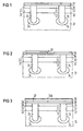
- a highly n + -doped buried layer 32 made of single-crystal silicon is produced on a substrate 31 made of p-doped monocrystalline silicon.
- a lower n-doped layer 33 made of single-crystal silicon is applied to the buried layer 32 (see FIG. 1).
- Channel stopper regions 34 and trenches 35 are formed in the substrate 31 according to the technique described in H. Goto, Springer Series in Electronics and Photonics, vol. 27, pp. 61-77.
- the trenches 35 cut through the n-doped layer 33 and the buried layer 32 and, together with the channel stopper regions 34, ensure reliable lateral insulation of adjacent transistors in the substrate.
- the n-doped layer 33 and the filled one Trenches 35 become an oxide layer 36 thermally as the first layer grew up.
- the oxide layer 36 is the second layer a polycrystalline silicon layer 37 is deposited.
- the polycrystalline silicon layer 37 is then z. B. with Boron p-doped.
- the polycrystalline silicon layer 37 is then structured (see FIG. 2). This is followed by a conformal deposition of an SiO 2 layer 38.
- the SiO 2 layer 38 is removed using a global planarizing method such as B. grinding or etching back over epoxy resin on the surface of the polycrystalline silicon layer 37 removed (see FIG. 3).
- the polycrystalline silicon layer 37 and the remnants of the SiO 2 layer 38 then form a common flat surface.
- An SiO 2 layer 39 is deposited thereon and an Si 3 N 4 layer 310 is deposited thereon (see FIG. 3).
- the Si 3 N 4 layer 310 is structured by anisotropic etching.
- a first area 311 and a second area 312 are defined. Both the first region 311 and the second region 312 lie within the trenches 35.
- the first region 311 lies completely above the polycrystalline silicon layer 37.
- the second region 312 lies completely to the side of the polycrystalline silicon layer 37.
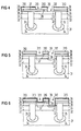
- anisotropic etching which attacks SiO 2 and is selective to silicon, the first region 311 is transferred into the SiO 2 layer 39 and the second region 312 into the SiO 2 layer 39, the SiO 2 layer 38 and the SiO 2 layer 36.
- the surface of the polycrystalline silicon layer 37 is exposed in the first region.
- the surface of the n-doped layer 33 which consists of monocrystalline silicon, is exposed (see FIG. 4). Since the etching is selective to the silicon, the polycrystalline silicon layer 37 and the n-doped silicon layer 33 act as an etching stop.
- the polycrystalline Silicon layer 37 structured.
- the one underneath works Oxide layer 36 as an etch stop.
- the n-doped layer 33 is structured in the second area 312 . It arises Caustic trench, at the bottom of which the surface of the buried Layer 32 is exposed. The depth of the etching trench is about the duration of the anisotropic silicon etching is set (see Fig. 5).
- Si 3 N 4 layer 313 is then deposited conformally over the entire surface (see FIG. 6).
- the Si 3 N 4 layer 313 is etched back by anisotropic etching selectively to silicon and SiO 2 , so that flank coverings 3131 on the exposed, vertical flanks of the Si 3 N 4 layer 310, the SiO 2 layer 39, and the polycrystalline silicon layer 37, the oxide layer 36 and the n-doped layer 33 arise (see FIG. 7).
- an isotropic, isotropic etching step that is selective for silicon and Si 3 N 4 , the oxide layer 36 is removed in the first region 311. The surface of the n-doped layer 33 is exposed.
- undercuts 314 are generated under the polycrystalline silicon layer 37. The depth of the undercuts 314 is adjusted over the etch duration. This etching does not cause any changes in the second region 312, since it does not attack silicon and Si 3 N 4 (see FIG. 7).
- Selective epitaxy is applied to the exposed surface of the n-doped layer 33 in the first region 311 and at the exposed surface of buried layer 32 in the second Area 312 each generated a single-crystal area 315.
- the single-crystal region 315 also grows the exposed surfaces of the polycrystalline layer 37 in the area of undercuts 314.
- the single-crystal region 315 in the first region 311 forms a basis for a finished bipolar transistor. Therefore, the single crystal region 315 is z. B. p-doped with a dopant concentration of about 1 ⁇ 10 18 cm 3 boron.
- the layer thickness here is in the range between 50 and 100 nm.
- Another possibility is to implement the single-crystalline region 315 doped with boron / germanium. The germanium content in silicon is around 20 to 40 atomic percent. In this case, a heterostructure base is formed.
- Another possibility is to grow the single-crystal region 315 with a low n-doping with a dopant concentration of approximately 1 ⁇ 10 16 cm 3 As.
- the single-crystalline region 315 then represents a continuation of a collector formed by the n-doped layer 33. In this case, the base is introduced by subsequent, unmasked implantation of boron.
- the Si 3 N 4 layer 310 and the flank coverings 3131 which served as etch protection for the layers underneath during the laterally acting isotropic SiO 2 etching (see FIG. 8), can remain on the structure or be removed.
- the first option has the advantage of saving process steps, while the latter option has the advantage that stresses caused by Si 3 N 4 are avoided.
- the polycrystalline silicon layer 317 is then anisotropically selectively etched back to the silicon oxide, with flank coverings 3171 (spacers) being produced (see FIG. 10).
- the oxide layer 316 acts as an etch stop.
- the exposed parts of the oxide layer 316 are then selectively removed wet-chemically to the silicon.
- the production of the flank coverings 3171 in this way by the deposition of first an oxide and then a polycrystalline silicon layer has the advantage over the production of a pure oxide spacer that there is no aftertreatment for the removal of polymers which are caused by SiO 2 dry etching on silicon substrates when realizing an oxide spacer arise, is necessary. This avoids the silicon attack during this polymer removal, which always takes place on the surface of the single-crystal region.
- a conformal deposition of a polycrystalline silicon layer 318 follows.
- the polycrystalline silicon layer 318 is deposited in such a thickness that both in the first region 311 and in the second region 312 the space between the opposite flank coverings 3171 is completely filled.
- the polycrystalline silicon layer 318 is n + doped. This is done e.g. B. by arsenic implantation or arsenic-doped deposition.
- the polycrystalline silicon layer 318 is etched back selectively to silicon oxide in an anisotropic etching step such that the height of the upper edge of the remaining polysilicon 3181 in the first region 311 and in the second region 312 approximately corresponds to the height of the upper edge of the polycrystalline layer 37 (see FIG. 11 ).
- the remaining polysilicon 3181 in the first region 311 forms an emitter connection, from which the emitter is formed by out-diffusion.
- the remaining polycrystalline silicon 3181 in the second region 312 forms a collector connection, which is connected via the buried layer 32, which acts as a buried collector connection, to the n-doped layer 33, which acts as a collector.
- the polycrystalline layer 37 forms the base connection, which is connected in the region of the undercuts 314 to the single-crystalline region 315 which forms the base in the first region 311. Since side wall defects and facets of the single-crystal region 315 lie in the region of the undercuts 314 and since high doping is achieved in this region by diffusion out of the base connection 37, these crystal defects are harmless for the finished bipolar transistor. According to a photolithographic definition (not shown), a base contact window 319 is opened by anisotropic etching in the SiO 2 layer 39, which extends through the SiO 2 layer 39 onto the polycrystalline silicon layer 37, which forms the base connection.
- the base contact window 319, the first area 311 and the second area 312 filled with tungsten is done e.g. B. by selective deposition or conformal Deposition followed by anisotropic etching back. Thereby complete planarity of the bipolar transistor is established (see Fig. 12).
- the structure is then with a passivation layer 321.
- contact holes are opened in a known manner and with metallizations 322 for connection as the base connection acting polycrystalline silicon layer 37, the as 3181 and polycrystalline silicon of the polycrystalline silicon acting as collector connection 3181 provided.
- the resulting bipolar transistor is only five Realized photo techniques, the first level of metallization is expected.
- the bipolar transistor has one Self-adjustment both with regard to the emitter / base and with regard to Base / collector on.
- the area that the base collector capacity defined is identical to that Area that determines the current flow through the collector. This Geometry represents the optimum with a minimal base collector capacity is achieved.
- the collector connection of the Bipolar transistor is made via a trench contact, which the The advantage is that the connection of the buried layer 32, the serves as a buried collector connection without significant The structure is exposed to high temperatures.
- the bipolar transistor has very high packing densities.
- MOS transistor has the advantage of being self-aligned To be source / drain and gate. Because the canal area is secluded the possibilities of delta-doped open up Profiles or hetero-junction profiles using SiGe.
Landscapes
- Bipolar Transistors (AREA)
- Thin Film Transistor (AREA)
- Insulated Gate Type Field-Effect Transistor (AREA)
- Metal-Oxide And Bipolar Metal-Oxide Semiconductor Integrated Circuits (AREA)
- Element Separation (AREA)
Description
- Fig. 1 bis Fig. 12
- zeigt Schritte eines Verfahrens zur Herstellung eines Bipolartransistors.
Claims (8)
- Verfahren zur Herstellung eines Bipolartransistors mit folgenden Schritten:a) in einem Substrat (31) aus einem einkristallinen Halbleitermaterial wird ein Kollektor (33) gebildet,b) auf dem Substrat (31) wird eine erste Schicht (36) aus SiO2 erzeugt, die selektiv zu dem Substrat (31) ätzbar ist,c) auf der ersten Schicht (36) wird eine zweite Schicht (37) aus polykristallinem Silizium erzeugt, zu der die erste Schicht (36) selektiv ätzbar ist,d) die zweite Schicht (37) wird so dotiert und strukturiert, daß sie einen Basisanschluß bildet,e) es wird ganzflächig und konform eine vierte Schicht (38) abgeschieden, die dieselben Ätzeigenschaften wie die erste Schicht (36) aufweist,f) die vierte Schicht (38) wird planarisiert, so daß die Oberfläche der zweiten Schicht (37) freigelegt wird,g) es wird eine Maske (310) erzeugt, die einen ersten Bereich (311) für Emitter, Basis und Kollektor und seitlich davon einen zweiten Bereich (312) für einen Kollektoranschluß definiert,h) in einem zu Silizium selektiven, anisotropen Ätzschritt wird die Oberfläche der zweiten Schicht (37) im ersten Bereich (311) und die Oberfläche des Substrats (31) im zweiten Bereich (312) freigelegt,i) in einem zu Siliziumoxid selektiven, anisotropen Ätzschritt wird im ersten Bereich (311) die zweite Schicht (37) entfernt und im zweiten Bereich (312) ein Ätzgraben in die Oberfläche des Substrats (33) erzeugt, dessen Tiefe über die Dauer des Ätzschritts gesteuert wird,j) mindestens die Flanken der zweiten Schicht werden mit einer dritten Schicht (310, 3131) bedeckt, an deren Oberfläche bei einer selektiven Epitaxie keine Keimbildung stattfindet und die den Ätzungen der ersten Schicht widersteht,k) die erste Schicht (36) wird so strukturiert, daß die Oberfläche des Substrats (11, 21, 31) im ersten Bereich freigelegt wird,l) in einem zum Substrat (31), zur zweiten Schicht (37) und zur dritten Schicht (310, 313) selektiven, isotropen Ätzschritt wird die Oberfläche des Substrats (31) innerhalb einer Unterätzung (314) der ersten Schicht (36) unter die zweite Schicht (37) freigelegt,m) mittels selektiver Epitaxie wird auf der freiliegenden Oberfläche des Substrats (31) im ersten Bereich (311) ein einkristallines Gebiet (315) erzeugt,n) in dem einkristallinen Gebiet (315) wird eine Basis gebildet,o) oberhalb der Basis (315) wird ein Emitter gebildet.
- Verfahren nach Anspruch 1 mit folgenden Schritten:a) nach der selektiven Epitaxie wird ganzflächig und konform eine Oxidschicht (316) und darauf ganzflächig und konform eine erste polykristalline Siliziumschicht (317) abgeschieden,b) in einem zu Siliziumoxid selektivem anisotropen Ätzschritt wird die erste polykristalline Siliziumschicht (317) so zurückgeätzt, daß an den senkrechten Flanken des ersten Bereichs (311) und des zweiten Bereichs (312) Flankenbedeckungen (3171) entstehen,c) die freiliegende Oxidschicht (316) wird selektiv zum Silizium naßchemisch entfernt.
- Verfahren nach Anspruch 2 mit folgenden Schritten:a) nach der Bildung der Flankenbedeckungen (3171) und der Freilegung der Siliziumoberfläche im ersten Bereich (311) und im zweiten Bereich (312) wird ganzflächig und konform eine zweite polykristalline Schicht (318) in einer solchen Dicke erzeugt, daß der erste Bereich (311) und der zweite Bereich (312) davon im wesentlichen aufgefüllt sind,b) in einem anisotropen Ätzschritt wird die zweite polykristalline Schicht (318) soweit zurückgeätzt, daß die Höhe des im ersten Bereich (311) und im zweiten Bereich (312) verbleibenden Teils der zweiten polykristallinen Schicht (3181) im wesentlichen der Höhe der als Basisanschluß wirkenden zweiten Schicht (37) entspricht.
- Verfahren nach einem der Ansprüche 1 bis 3,
bei dem das einkristalline Gebiet (314) durch Zugabe von Dotierstoff enthaltenden Verbindungen bei der selektiven Epitaxie in situ dotiert wird. - Verfahren nach einem der Ansprüche 1 bis 4,
bei dem ein Substrat (31) aus einkristallinem Silizium verwendet wird. - Verfahren nach Anspruch 5,
bei dem das einkristalline Gebiet (314) aus Si1-xGex mit x zwischen 0,2 und 0,4 gebildet wird. - Verfahren nach einem der Ansprüche 1 bis 6,
bei dem die dritte Schicht (310, 3131) nach der selektiven Epitaxie vollständig entfernt wird. - Verfahren nach einem der Ansprüche 1 bis 7,
bei dem die dritte Schicht (310, 3131) aus Si3N4 und die vierte Schicht (38) aus SiO2 gebildet werden.
Priority Applications (1)
| Application Number | Priority Date | Filing Date | Title |
|---|---|---|---|
| EP97114782A EP0809279B1 (de) | 1991-09-23 | 1992-08-19 | Verfahren zur Herstellung eines MOS-Transistors |
Applications Claiming Priority (2)
| Application Number | Priority Date | Filing Date | Title |
|---|---|---|---|
| DE4131619 | 1991-09-23 | ||
| DE4131619 | 1991-09-23 |
Related Child Applications (1)
| Application Number | Title | Priority Date | Filing Date |
|---|---|---|---|
| EP97114782A Division EP0809279B1 (de) | 1991-09-23 | 1992-08-19 | Verfahren zur Herstellung eines MOS-Transistors |
Publications (3)
| Publication Number | Publication Date |
|---|---|
| EP0535350A2 EP0535350A2 (de) | 1993-04-07 |
| EP0535350A3 EP0535350A3 (en) | 1993-09-08 |
| EP0535350B1 true EP0535350B1 (de) | 1998-04-08 |
Family
ID=6441263
Family Applications (2)
| Application Number | Title | Priority Date | Filing Date |
|---|---|---|---|
| EP97114782A Expired - Lifetime EP0809279B1 (de) | 1991-09-23 | 1992-08-19 | Verfahren zur Herstellung eines MOS-Transistors |
| EP92114161A Expired - Lifetime EP0535350B1 (de) | 1991-09-23 | 1992-08-19 | Verfahren zur Herstellung eines seitlich begrenzten, einkristallinen Gebietes in einem Bipolartransistor |
Family Applications Before (1)
| Application Number | Title | Priority Date | Filing Date |
|---|---|---|---|
| EP97114782A Expired - Lifetime EP0809279B1 (de) | 1991-09-23 | 1992-08-19 | Verfahren zur Herstellung eines MOS-Transistors |
Country Status (4)
| Country | Link |
|---|---|
| US (3) | US5326718A (de) |
| EP (2) | EP0809279B1 (de) |
| JP (1) | JPH05206460A (de) |
| DE (2) | DE59209978D1 (de) |
Cited By (2)
| Publication number | Priority date | Publication date | Assignee | Title |
|---|---|---|---|---|
| DE19958062C2 (de) * | 1999-12-02 | 2002-06-06 | Infineon Technologies Ag | Verfahren zur Herstellung eines Bipolartransistors und Verfahren zur Herstellung einer integrierten Schaltungsanordnung mit einem solchen Bipolartransistor |
| DE10231407B4 (de) * | 2002-07-11 | 2007-01-11 | Infineon Technologies Ag | Bipolartransistor |
Families Citing this family (33)
| Publication number | Priority date | Publication date | Assignee | Title |
|---|---|---|---|---|
| DE4314906C2 (de) * | 1993-05-05 | 1996-10-31 | Siemens Ag | Halbleiterbauelement mit Stromanschlüssen für hohe Integrationsdichte |
| US5532188A (en) * | 1994-03-30 | 1996-07-02 | Wright; Peter J. | Global planarization of multiple layers |
| US5994718A (en) * | 1994-04-15 | 1999-11-30 | National Semiconductor Corporation | Trench refill with selective polycrystalline materials |
| JP2720793B2 (ja) * | 1994-05-12 | 1998-03-04 | 日本電気株式会社 | 半導体装置の製造方法 |
| US5484737A (en) * | 1994-12-13 | 1996-01-16 | Electronics & Telecommunications Research Institute | Method for fabricating bipolar transistor |
| US5668025A (en) * | 1995-02-28 | 1997-09-16 | Sgs-Thomson Microelectronics, Inc. | Method of making a FET with dielectrically isolated sources and drains |
| US6420764B1 (en) | 1995-02-28 | 2002-07-16 | Stmicroelectronics, Inc. | Field effect transitor having dielectrically isolated sources and drains and methods for making same |
| US5773328A (en) | 1995-02-28 | 1998-06-30 | Sgs-Thomson Microelectronics, Inc. | Method of making a fully-dielectric-isolated fet |
| WO1997015071A1 (en) * | 1995-10-20 | 1997-04-24 | Philips Electronics N.V. | Manufacture of a semiconductor device with selectively deposited semiconductor zone |
| JP4150076B2 (ja) * | 1996-03-29 | 2008-09-17 | エヌエックスピー ビー ヴィ | 半導体装置の製造方法 |
| KR100218668B1 (ko) * | 1996-12-14 | 1999-09-01 | 권혁준 | 바이폴라 소자의 컬랙터 장치 및 그 제조방법 |
| KR100215841B1 (ko) * | 1997-04-10 | 1999-08-16 | 구본준 | 바이폴라소자 제조방법 |
| US6198114B1 (en) | 1997-10-28 | 2001-03-06 | Stmicroelectronics, Inc. | Field effect transistor having dielectrically isolated sources and drains and method for making same |
| US6180978B1 (en) * | 1997-12-30 | 2001-01-30 | Texas Instruments Incorporated | Disposable gate/replacement gate MOSFETs for sub-0.1 micron gate length and ultra-shallow junctions |
| US6207515B1 (en) * | 1998-05-27 | 2001-03-27 | Taiwan Semiconductor Manufacturing Company | Method of fabricating buried source to shrink chip size in memory array |
| DE19845792A1 (de) * | 1998-09-21 | 2000-03-23 | Inst Halbleiterphysik Gmbh | Verfahren zur Erzeugung einer amorphen oder polykristallinen Schicht auf einem Isolatorgebiet |
| DE19845789A1 (de) * | 1998-09-21 | 2000-03-23 | Inst Halbleiterphysik Gmbh | Bipolartransistor und Verfahren zu seiner Herstellung |
| JP2001068673A (ja) * | 1999-07-21 | 2001-03-16 | Motorola Inc | 半導体装置の形成方法 |
| JP2001118857A (ja) | 1999-10-15 | 2001-04-27 | Matsushita Electronics Industry Corp | 横型バイポーラトランジスタ及びその製造方法 |
| DE10005442A1 (de) | 2000-02-08 | 2001-08-16 | Infineon Technologies Ag | Bipolartransistor |
| EP1152462A1 (de) * | 2000-05-05 | 2001-11-07 | Infineon Technologies AG | Verfahren zur Herstellung eines Bipolartransistors |
| TW512529B (en) | 2000-06-14 | 2002-12-01 | Infineon Technologies Ag | Silicon bipolar transistor, circuit arrangement and method for producing a silicon bipolar transistor |
| US6972472B1 (en) * | 2002-04-02 | 2005-12-06 | Fairchild Semiconductor Corporation | Quasi self-aligned single polysilicon bipolar active device with intentional emitter window undercut |
| US7151035B2 (en) * | 2002-04-16 | 2006-12-19 | Renesas Technology Corp. | Semiconductor device and manufacturing method thereof |
| KR100485177B1 (ko) * | 2002-12-05 | 2005-04-22 | 동부아남반도체 주식회사 | 모스 트랜지스터 및 그 제조 방법 |
| KR100505113B1 (ko) * | 2003-04-23 | 2005-07-29 | 삼성전자주식회사 | 모스 트랜지스터 및 그 제조방법 |
| US6891229B2 (en) * | 2003-04-30 | 2005-05-10 | Freescale Semiconductor, Inc. | Inverted isolation formed with spacers |
| US6924202B2 (en) * | 2003-10-09 | 2005-08-02 | Chartered Semiconductor Manufacturing, Ltd. | Heterojunction bipolar transistor with self-aligned emitter and sidewall base contact |
| US8435873B2 (en) | 2006-06-08 | 2013-05-07 | Texas Instruments Incorporated | Unguarded Schottky barrier diodes with dielectric underetch at silicide interface |
| KR101588852B1 (ko) * | 2008-10-31 | 2016-01-26 | 삼성전자주식회사 | 반도체 소자 및 그 형성방법 |
| DE102016216084B8 (de) | 2016-08-26 | 2021-12-23 | Infineon Technologies Dresden Gmbh | Verfahren zum Herstellen eines Bipolartransistors |
| KR101886324B1 (ko) * | 2016-11-03 | 2018-08-20 | 주식회사 그라피아 | Led 디스플레이 구조체 및 그 제조방법 |
| US11295983B2 (en) | 2020-05-27 | 2022-04-05 | International Business Machines Corporation | Transistor having source or drain formation assistance regions with improved bottom isolation |
Family Cites Families (33)
| Publication number | Priority date | Publication date | Assignee | Title |
|---|---|---|---|---|
| JPS5539677A (en) * | 1978-09-14 | 1980-03-19 | Chiyou Lsi Gijutsu Kenkyu Kumiai | Semiconductor device and its manufacturing |
| JPS577959A (en) * | 1980-06-19 | 1982-01-16 | Toshiba Corp | Semiconductor device |
| US4324038A (en) * | 1980-11-24 | 1982-04-13 | Bell Telephone Laboratories, Incorporated | Method of fabricating MOS field effect transistors |
| US4483726A (en) * | 1981-06-30 | 1984-11-20 | International Business Machines Corporation | Double self-aligned fabrication process for making a bipolar transistor structure having a small polysilicon-to-extrinsic base contact area |
| US5296391A (en) * | 1982-03-24 | 1994-03-22 | Nec Corporation | Method of manufacturing a bipolar transistor having thin base region |
| US4554570A (en) * | 1982-06-24 | 1985-11-19 | Rca Corporation | Vertically integrated IGFET device |
| US4529455A (en) * | 1983-10-28 | 1985-07-16 | At&T Bell Laboratories | Method for epitaxially growing Gex Si1-x layers on Si utilizing molecular beam epitaxy |
| US4614564A (en) * | 1984-12-04 | 1986-09-30 | The United States Of America As Represented By The United States Department Of Energy | Process for selectively patterning epitaxial film growth on a semiconductor substrate |
| JPS61164262A (ja) * | 1985-01-17 | 1986-07-24 | Toshiba Corp | 半導体装置 |
| JPS6252963A (ja) * | 1985-09-02 | 1987-03-07 | Fujitsu Ltd | バイポ−ラトランジスタの製造方法 |
| JPH0622238B2 (ja) * | 1985-10-02 | 1994-03-23 | 沖電気工業株式会社 | バイポ−ラ型半導体集積回路装置の製造方法 |
| KR900007686B1 (ko) * | 1986-10-08 | 1990-10-18 | 후지쓰 가부시끼가이샤 | 선택적으로 산화된 실리콘 기판상에 에피택셜 실리콘층과 다결정 실리콘층을 동시에 성장시키는 기상 증착방법 |
| US4832837A (en) * | 1987-04-13 | 1989-05-23 | Frederick Loren D | Apparatus for augmenting separation of oil and water |
| US4757029A (en) * | 1987-05-04 | 1988-07-12 | Motorola Inc. | Method of making vertical field effect transistor with plurality of gate input cnnections |
| DE3825701A1 (de) * | 1987-07-29 | 1989-02-09 | Toshiba Kawasaki Kk | Verfahren zur herstellung eines bipolaren transistors |
| US5296087A (en) * | 1987-08-24 | 1994-03-22 | Canon Kabushiki Kaisha | Crystal formation method |
| US4786615A (en) * | 1987-08-31 | 1988-11-22 | Motorola Inc. | Method for improved surface planarity in selective epitaxial silicon |
| US4818713A (en) * | 1987-10-20 | 1989-04-04 | American Telephone And Telegraph Company, At&T Bell Laboratories | Techniques useful in fabricating semiconductor devices having submicron features |
| KR890011103A (ko) * | 1987-12-04 | 1989-08-12 | 미다 가쓰시게 | 반도체 집적회로장치의 제조방법 |
| JP2728671B2 (ja) * | 1988-02-03 | 1998-03-18 | 株式会社東芝 | バイポーラトランジスタの製造方法 |
| FR2629637B1 (fr) * | 1988-04-05 | 1990-11-16 | Thomson Csf | Procede de realisation d'une alternance de couches de materiau semiconducteur monocristallin et de couches de materiau isolant |
| FR2629636B1 (fr) * | 1988-04-05 | 1990-11-16 | Thomson Csf | Procede de realisation d'une alternance de couches de materiau semiconducteur monocristallin et de couches de materiau isolant |
| US5204276A (en) * | 1988-12-06 | 1993-04-20 | Kabushiki Kaisha Toshiba | Method of manufacturing semiconductor device |
| US5024957A (en) * | 1989-02-13 | 1991-06-18 | International Business Machines Corporation | Method of fabricating a bipolar transistor with ultra-thin epitaxial base |
| JPH0744186B2 (ja) * | 1989-03-13 | 1995-05-15 | 株式会社東芝 | 半導体装置の製造方法 |
| US5008207A (en) * | 1989-09-11 | 1991-04-16 | International Business Machines Corporation | Method of fabricating a narrow base transistor |
| DE58909884D1 (de) * | 1989-09-22 | 2002-02-14 | Infineon Technologies Ag | CMOS-kompatibler Bipolartransistor mit verringerter Kollektor/Substrat-Kapazität und Verfahren zu dessen Herstellung |
| JPH03209833A (ja) * | 1989-12-01 | 1991-09-12 | Hewlett Packard Co <Hp> | 先進的エピタキシャル堆積技術を利用したSi/SiGe異種接合バイポーラトランジスタ及びその製造方法 |
| US5126285A (en) * | 1990-07-02 | 1992-06-30 | Motorola, Inc. | Method for forming a buried contact |
| US5028557A (en) * | 1990-08-27 | 1991-07-02 | Taiwan Semiconductor Manufacturing Co., Ltd. | Method of making a reverse self-aligned BIMOS transistor integrated circuit |
| KR920017269A (ko) * | 1991-02-21 | 1992-09-26 | 김광호 | 다결정실리콘 재충전(refill)법을 이용한 Laterally Graded Emitter(LGE)구조의 바이폴라 트랜지스터 제조방법 |
| US5198375A (en) * | 1992-03-23 | 1993-03-30 | Motorola Inc. | Method for forming a bipolar transistor structure |
| US5340754A (en) * | 1992-09-02 | 1994-08-23 | Motorla, Inc. | Method for forming a transistor having a dynamic connection between a substrate and a channel region |
-
1992
- 1992-08-19 EP EP97114782A patent/EP0809279B1/de not_active Expired - Lifetime
- 1992-08-19 DE DE59209978T patent/DE59209978D1/de not_active Expired - Lifetime
- 1992-08-19 DE DE59209271T patent/DE59209271D1/de not_active Expired - Lifetime
- 1992-08-19 EP EP92114161A patent/EP0535350B1/de not_active Expired - Lifetime
- 1992-09-18 JP JP4275293A patent/JPH05206460A/ja active Pending
- 1992-09-23 US US07/950,068 patent/US5326718A/en not_active Expired - Lifetime
-
1994
- 1994-01-24 US US08/185,514 patent/US5422303A/en not_active Expired - Lifetime
-
1995
- 1995-04-03 US US08/379,861 patent/US5498567A/en not_active Expired - Lifetime
Cited By (2)
| Publication number | Priority date | Publication date | Assignee | Title |
|---|---|---|---|---|
| DE19958062C2 (de) * | 1999-12-02 | 2002-06-06 | Infineon Technologies Ag | Verfahren zur Herstellung eines Bipolartransistors und Verfahren zur Herstellung einer integrierten Schaltungsanordnung mit einem solchen Bipolartransistor |
| DE10231407B4 (de) * | 2002-07-11 | 2007-01-11 | Infineon Technologies Ag | Bipolartransistor |
Also Published As
| Publication number | Publication date |
|---|---|
| US5422303A (en) | 1995-06-06 |
| EP0535350A2 (de) | 1993-04-07 |
| DE59209271D1 (de) | 1998-05-14 |
| EP0809279B1 (de) | 2003-02-19 |
| DE59209978D1 (de) | 2003-03-27 |
| EP0535350A3 (en) | 1993-09-08 |
| EP0809279A3 (de) | 1998-08-05 |
| JPH05206460A (ja) | 1993-08-13 |
| US5326718A (en) | 1994-07-05 |
| EP0809279A2 (de) | 1997-11-26 |
| US5498567A (en) | 1996-03-12 |
Similar Documents
| Publication | Publication Date | Title |
|---|---|---|
| EP0535350B1 (de) | Verfahren zur Herstellung eines seitlich begrenzten, einkristallinen Gebietes in einem Bipolartransistor | |
| EP0600276B1 (de) | Verfahren zur Herstellung eines seitlich begrenzten, einkristallinen Gebietes mittels selektiver Epitaxie und dessen Anwendung zur Herstellung eines Bipolartransistors sowie eines MOS-transistors | |
| DE3784958T2 (de) | Seitenwanddistanzschichten zur Spannungsaufnahme und Isolierung von CMOS Schaltungen und Herstellungsverfahren. | |
| EP0000897B1 (de) | Verfahren zum Herstellen von lateral isolierten Siliciumbereichen | |
| DE102005046711B4 (de) | Verfahren zur Herstellung eines vertikalen MOS-Halbleiterbauelementes mit dünner Dielektrikumsschicht und tiefreichenden vertikalen Abschnitten | |
| EP1825504B1 (de) | Vertikaler bipolartransistor | |
| EP1597770A1 (de) | Bipolartransistor mit verbessertem basis-emitter- bergang und verfahren zur herstellung | |
| DE10004067A1 (de) | Verfahren zum Herstellen eines Bipolarelementes und Bipolarelement | |
| DE4102888A1 (de) | Verfahren zur herstellung eines miniaturisierten heterouebergang-bipolartransistors | |
| DE102008001535A1 (de) | Bipolartransistor und Verfahren zur Herstellung desselben | |
| DE4444776C2 (de) | Verfahren zur Herstellung eines Bipolartransistors mit einer selbstjustierenden vertikalen Struktur | |
| EP0684639A1 (de) | Verfahren zur Herstellung eines Bipolartransistors | |
| DE69022832T2 (de) | Verfahren zur Bildung einer Germanium-Schicht und durch diese Schicht hergestellter Heteroübergangs-Bipolartransistor. | |
| EP1138085A2 (de) | Feldeffektgesteuerter transistor und verfahren zu dessen herstellung | |
| EP1145320A1 (de) | Dram-zellenanordnung und verfahren zur deren herstellung | |
| DE102005020410A1 (de) | Transistorstruktur und zugehöriges Herstellungsverfahren | |
| DE102020126638A1 (de) | Diffusionssperrschicht für source/ drain-strukturen zur erhöhung von transistorleistung | |
| EP1129482B1 (de) | Verfahren zur Herstellung von einer DRAM-Zellenanordnung | |
| EP1356527B1 (de) | Bipolartransistor und verfahren zu dessen herstellung | |
| DE102015204411B4 (de) | Transistor und Verfahren zur Herstellung eines Transistors | |
| DE2401380A1 (de) | Verfahren zur herstellung einer duennen einkristallinen siliciumschicht hoher qualitaet auf einer isolierenden substratschicht sowie halbleiteranordnung mit einer duennen hochqualitativen monokristallinen siliciumschicht | |
| DE69637500T2 (de) | Bipolartransistor mit epitaxialer Basis und Verfahren zur Herstellung | |
| DE10337561B4 (de) | Herstellungsverfahren für ein DRAM mit verbessertem Leckstromverhalten | |
| DE10038955C2 (de) | Verfahren zur Herstellung eines Bipolartransistors | |
| EP1701386A1 (de) | Verfahren zur Integration von zwei Bipolartransistoren in einem Halbleiterkörper, Halbleiteranordnung in einem Halbleiterkörper und Kaskodenschaltung |
Legal Events
| Date | Code | Title | Description |
|---|---|---|---|
| PUAI | Public reference made under article 153(3) epc to a published international application that has entered the european phase |
Free format text: ORIGINAL CODE: 0009012 |
|
| AK | Designated contracting states |
Kind code of ref document: A2 Designated state(s): BE DE FR GB IT |
|
| PUAL | Search report despatched |
Free format text: ORIGINAL CODE: 0009013 |
|
| AK | Designated contracting states |
Kind code of ref document: A3 Designated state(s): BE DE FR GB IT |
|
| 17P | Request for examination filed |
Effective date: 19931105 |
|
| 17Q | First examination report despatched |
Effective date: 19950309 |
|
| GRAG | Despatch of communication of intention to grant |
Free format text: ORIGINAL CODE: EPIDOS AGRA |
|
| GRAG | Despatch of communication of intention to grant |
Free format text: ORIGINAL CODE: EPIDOS AGRA |
|
| GRAH | Despatch of communication of intention to grant a patent |
Free format text: ORIGINAL CODE: EPIDOS IGRA |
|
| GRAH | Despatch of communication of intention to grant a patent |
Free format text: ORIGINAL CODE: EPIDOS IGRA |
|
| GRAA | (expected) grant |
Free format text: ORIGINAL CODE: 0009210 |
|
| DX | Miscellaneous (deleted) | ||
| AK | Designated contracting states |
Kind code of ref document: B1 Designated state(s): BE DE FR GB IT |
|
| REF | Corresponds to: |
Ref document number: 59209271 Country of ref document: DE Date of ref document: 19980514 |
|
| ET | Fr: translation filed | ||
| ITF | It: translation for a ep patent filed | ||
| GBT | Gb: translation of ep patent filed (gb section 77(6)(a)/1977) |
Effective date: 19980609 |
|
| PLBE | No opposition filed within time limit |
Free format text: ORIGINAL CODE: 0009261 |
|
| 26N | No opposition filed | ||
| REG | Reference to a national code |
Ref country code: GB Ref legal event code: IF02 |
|
| PGFP | Annual fee paid to national office [announced via postgrant information from national office to epo] |
Ref country code: DE Payment date: 20101014 Year of fee payment: 19 |
|
| REG | Reference to a national code |
Ref country code: GB Ref legal event code: 732E Free format text: REGISTERED BETWEEN 20110707 AND 20110713 |
|
| REG | Reference to a national code |
Ref country code: FR Ref legal event code: TP Owner name: INFINEON TECHNOLOGIES AG, DE Effective date: 20110922 |
|
| PGFP | Annual fee paid to national office [announced via postgrant information from national office to epo] |
Ref country code: FR Payment date: 20110901 Year of fee payment: 20 Ref country code: GB Payment date: 20110819 Year of fee payment: 20 |
|
| REG | Reference to a national code |
Ref country code: DE Ref legal event code: R081 Ref document number: 59209271 Country of ref document: DE Owner name: INFINEON TECHNOLOGIES AG, DE Free format text: FORMER OWNER: SIEMENS AG, 80333 MUENCHEN, DE Effective date: 20111107 Ref country code: DE Ref legal event code: R081 Ref document number: 59209271 Country of ref document: DE Owner name: INFINEON TECHNOLOGIES AG, DE Free format text: FORMER OWNER: SIEMENS AKTIENGESELLSCHAFT, 80333 MUENCHEN, DE Effective date: 20111107 |
|
| PGFP | Annual fee paid to national office [announced via postgrant information from national office to epo] |
Ref country code: IT Payment date: 20110824 Year of fee payment: 20 Ref country code: BE Payment date: 20110811 Year of fee payment: 20 |
|
| REG | Reference to a national code |
Ref country code: DE Ref legal event code: R071 Ref document number: 59209271 Country of ref document: DE |
|
| REG | Reference to a national code |
Ref country code: DE Ref legal event code: R071 Ref document number: 59209271 Country of ref document: DE |
|
| BE20 | Be: patent expired |
Owner name: *SIEMENS A.G. Effective date: 20120819 |
|
| REG | Reference to a national code |
Ref country code: GB Ref legal event code: PE20 Expiry date: 20120818 |
|
| PG25 | Lapsed in a contracting state [announced via postgrant information from national office to epo] |
Ref country code: GB Free format text: LAPSE BECAUSE OF EXPIRATION OF PROTECTION Effective date: 20120818 Ref country code: DE Free format text: LAPSE BECAUSE OF EXPIRATION OF PROTECTION Effective date: 20120821 |