EP0532025B1 - Dispositif semi-conducteur optique ayant un laser à semi-conducteur et un photodétecteur - Google Patents
Dispositif semi-conducteur optique ayant un laser à semi-conducteur et un photodétecteur Download PDFInfo
- Publication number
- EP0532025B1 EP0532025B1 EP92115573A EP92115573A EP0532025B1 EP 0532025 B1 EP0532025 B1 EP 0532025B1 EP 92115573 A EP92115573 A EP 92115573A EP 92115573 A EP92115573 A EP 92115573A EP 0532025 B1 EP0532025 B1 EP 0532025B1
- Authority
- EP
- European Patent Office
- Prior art keywords
- layer
- semiconductor device
- photodetector
- optical semiconductor
- optical
- Prior art date
- Legal status (The legal status is an assumption and is not a legal conclusion. Google has not performed a legal analysis and makes no representation as to the accuracy of the status listed.)
- Expired - Lifetime
Links
Images


Classifications
-
- H—ELECTRICITY
- H01—ELECTRIC ELEMENTS
- H01S—DEVICES USING THE PROCESS OF LIGHT AMPLIFICATION BY STIMULATED EMISSION OF RADIATION [LASER] TO AMPLIFY OR GENERATE LIGHT; DEVICES USING STIMULATED EMISSION OF ELECTROMAGNETIC RADIATION IN WAVE RANGES OTHER THAN OPTICAL
- H01S5/00—Semiconductor lasers
- H01S5/30—Structure or shape of the active region; Materials used for the active region
-
- H—ELECTRICITY
- H01—ELECTRIC ELEMENTS
- H01L—SEMICONDUCTOR DEVICES NOT COVERED BY CLASS H10
- H01L27/00—Devices consisting of a plurality of semiconductor or other solid-state components formed in or on a common substrate
- H01L27/15—Devices consisting of a plurality of semiconductor or other solid-state components formed in or on a common substrate including semiconductor components with at least one potential-jump barrier or surface barrier specially adapted for light emission
-
- H—ELECTRICITY
- H01—ELECTRIC ELEMENTS
- H01S—DEVICES USING THE PROCESS OF LIGHT AMPLIFICATION BY STIMULATED EMISSION OF RADIATION [LASER] TO AMPLIFY OR GENERATE LIGHT; DEVICES USING STIMULATED EMISSION OF ELECTROMAGNETIC RADIATION IN WAVE RANGES OTHER THAN OPTICAL
- H01S5/00—Semiconductor lasers
- H01S5/02—Structural details or components not essential to laser action
- H01S5/026—Monolithically integrated components, e.g. waveguides, monitoring photo-detectors, drivers
- H01S5/0262—Photo-diodes, e.g. transceiver devices, bidirectional devices
- H01S5/0264—Photo-diodes, e.g. transceiver devices, bidirectional devices for monitoring the laser-output
Claims (12)
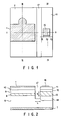
- Dispositif à semiconducteur optique comprenant un substrat semiconducteur (6), un laser à semiconducteur (6, 8, 9, 10) prévu sur le substrat semiconducteur (6) et incluant une structure en forme de bande comportant une couche active (8), une couche de blocage de courant (5, 4, 3, 2) prévue sur le substrat semiconducteur (6) de manière à enterrer le laser à semiconducteur (6, 8, 9, 10), un photodétecteur (14, 13, 12, 11) prévu sur le substrat semiconducteur (6) et une gorge (17) prévue dans le substrat semiconducteur (6) pour définir une surface d'extrémité d'émission du laser à semiconducteur et une surface de détection de lumière du photodétecteur se faisant face l'une l'autre, caractérisé en ce que le photodétecteur présente la même épaisseur et la même composition que celles de la couche de blocage de courant (5, 4, 3, 2).
- Dispositif à semiconducteur optique selon la revendication 1, caractérisé en ce que la couche de blocage de courant (5, 4, 3, 2) et le photodétecteur (14, 13, 12, 11) incluent une couche semiconductrice de type i (4, 13).
- Dispositif à semiconducteur optique selon la revendication 2, caractérisé en ce que la couche semiconductrice de type i (13) du photodétecteur constitue une couche d'absorption de lumière.
- Dispositif à semiconducteur optique selon la revendication 3, caractérisé en ce qu'une épaisseur H de la couche d'absorption de lumière (13) est supérieure à celle de la couche active (8).
- Dispositif à semiconducteur optique selon la revendication 1, caractérisé en ce qu'une première électrode positive (1) est prévue sur le laser à semiconducteur tandis qu'une seconde électrode positive (16) est disposée sur le photodétecteur.
- Dispositif à semiconducteur optique selon la revendication 1, caractérisé en ce qu'une électrode négative (7) est prévue sur le substrat semiconducteur (6) en tant qu'électrode commune.
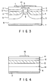
- Dispositif à semiconducteur optique selon la revendication 4, caractérisé en ce que l'épaisseur H de la couche d'absorption de lumière (13) est donnée par H = L tan (θ/2) où L est une largeur de la gorge (17) et θ est un angle de rayonnement d'un faisceau laser émis depuis le laser à semiconducteur.
- Dispositif à semiconducteur optique selon la revendication 5, caractérisé en ce que la première électrode positive (1) et la seconde électrode positive (16) sont agencées de telle sorte qu'une ligne centrale des première et seconde électrodes positives (1, 16) corresponde à un axe optique.
- Dispositif à semiconducteur optique selon la revendication 5, caractérisé en ce qu'une distance l1 entre la surface de détection de lumière et un côté de la seconde électrode positive (16) est inférieure à une distance l3 entre une surface d'extrémité du photodétecteur et un côté opposé de la seconde électrode positive (16).
- Dispositif à semiconducteur optique selon la revendication 1, caractérisé en ce que la surface de détection de lumière du photodétecteur est inclinée selon un angle de 5 à 20 degrés par rapport à la surface d'extrémité d'émission.
- Dispositif à semiconducteur optique selon la revendication 2, caractérisé en ce que la couche semiconductrice de type i (4, 13) présente une énergie de bande interdite inférieure à celle de la couche active (8).
- Dispositif à semiconducteur optique selon la revendication 2, caractérisé en ce que la couche de blocage de courant et le photodétecteur présentent une structure choisie parmi les structures n-p-i-n, n-i-p-n, n-i-p, et n-i-n.
Applications Claiming Priority (2)
| Application Number | Priority Date | Filing Date | Title |
|---|---|---|---|
| JP26048791A JP2980435B2 (ja) | 1991-09-12 | 1991-09-12 | 半導体装置 |
| JP260487/91 | 1991-09-12 |
Publications (2)
| Publication Number | Publication Date |
|---|---|
| EP0532025A1 EP0532025A1 (fr) | 1993-03-17 |
| EP0532025B1 true EP0532025B1 (fr) | 1997-01-02 |
Family
ID=17348651
Family Applications (1)
| Application Number | Title | Priority Date | Filing Date |
|---|---|---|---|
| EP92115573A Expired - Lifetime EP0532025B1 (fr) | 1991-09-12 | 1992-09-11 | Dispositif semi-conducteur optique ayant un laser à semi-conducteur et un photodétecteur |
Country Status (5)
| Country | Link |
|---|---|
| US (1) | US5281829A (fr) |
| EP (1) | EP0532025B1 (fr) |
| JP (1) | JP2980435B2 (fr) |
| KR (1) | KR960005580B1 (fr) |
| DE (1) | DE69216329T2 (fr) |
Families Citing this family (18)
| Publication number | Priority date | Publication date | Assignee | Title |
|---|---|---|---|---|
| JPH0669491A (ja) * | 1992-08-18 | 1994-03-11 | Fujitsu Ltd | 光送受信装置 |
| DE19502252A1 (de) * | 1994-01-26 | 1995-07-27 | Ahlers Horst Dr Ing Habil | Temperatursensor |
| DE19812199C1 (de) * | 1998-03-19 | 1999-11-04 | Siemens Ag | Verfahren zur Herstellung einer Halbleiteranordnung und eine mindestens zwei Halbleiterelemente umfassende Halbleiteranordnung |
| US6137123A (en) * | 1999-08-17 | 2000-10-24 | Honeywell International Inc. | High gain GaN/AlGaN heterojunction phototransistor |
| KR100490921B1 (ko) * | 1999-10-30 | 2005-05-19 | 충남대학교산학협력단 | 순무피클의 제조방법 |
| US6265237B1 (en) * | 1999-12-15 | 2001-07-24 | Lucent Technologies Inc. | In-wafer testing of DFB semiconductor lasers |
| US7009210B2 (en) * | 2000-10-06 | 2006-03-07 | Alphion Corporation | Method and apparatus for bit-rate and format insensitive performance monitoring of lightwave signals |
| US6888171B2 (en) * | 2000-12-22 | 2005-05-03 | Dallan Luming Science & Technology Group Co., Ltd. | Light emitting diode |
| KR20010025701A (ko) * | 2001-01-18 | 2001-04-06 | 임준호 | 생오이를 이용한 피클 제조방법 |
| GB2389957A (en) * | 2002-06-19 | 2003-12-24 | Kamelian Ltd | Automatic power control of a semiconductor optical amplifier |
| JP4134695B2 (ja) * | 2002-11-21 | 2008-08-20 | 住友電気工業株式会社 | 光モジュール |
| KR100493089B1 (ko) * | 2002-12-17 | 2005-06-02 | 삼성전자주식회사 | 집적광학장치 |
| DE10345555A1 (de) | 2003-09-30 | 2005-05-04 | Osram Opto Semiconductors Gmbh | Strahlungsemittierendes und -empfangendes Halbleiterbauelement und Verfahren zu dessen Herstellung |
| KR100750506B1 (ko) * | 2004-12-10 | 2007-08-20 | 한국전자통신연구원 | 광감지기를 구비한 표면방출레이저소자 및 이를 적용한광도파로 소자 |
| JP4706970B2 (ja) * | 2006-02-16 | 2011-06-22 | 古河電気工業株式会社 | フォトニック結晶半導体光増幅器および集積型光半導体素子 |
| JP2009283822A (ja) | 2008-05-26 | 2009-12-03 | Mitsubishi Electric Corp | 半導体レーザ及びその製造方法 |
| DE102009028909A1 (de) | 2009-08-26 | 2011-03-17 | Nanoplus Gmbh Nanosystems And Technologies | Halbleiterlaser mit auf einem Laserspiegel angebrachtem Absorber |
| KR102607820B1 (ko) * | 2022-10-13 | 2023-11-29 | 서미수 | 다종의 야채와 과일을 포함하는 발효 피클 제조 방법 |
Family Cites Families (9)
| Publication number | Priority date | Publication date | Assignee | Title |
|---|---|---|---|---|
| JPS55148482A (en) * | 1979-05-08 | 1980-11-19 | Canon Inc | Semiconductor laser device |
| JPS5831593A (ja) * | 1981-08-18 | 1983-02-24 | Nec Corp | 光集積化素子 |
| DE3280183D1 (de) * | 1981-11-30 | 1990-06-28 | Fujitsu Ltd | Optische halbleiteranordnung. |
| JPS58186986A (ja) * | 1982-04-27 | 1983-11-01 | Kokusai Denshin Denwa Co Ltd <Kdd> | モニタ付分布帰還形半導体レ−ザ |
| JPS61140189A (ja) * | 1984-12-12 | 1986-06-27 | Canon Inc | 半導体レ−ザ |
| JPS61183988A (ja) * | 1985-02-08 | 1986-08-16 | Matsushita Electric Ind Co Ltd | 半導体レ−ザ装置 |
| JPS62145791A (ja) * | 1985-12-20 | 1987-06-29 | Agency Of Ind Science & Technol | 半導体装置 |
| JPS62150795A (ja) * | 1985-12-24 | 1987-07-04 | Mitsubishi Electric Corp | 半導体光素子構造 |
| JPS6360563A (ja) * | 1986-08-29 | 1988-03-16 | Nec Corp | 光電子集積素子 |
-
1991
- 1991-09-12 JP JP26048791A patent/JP2980435B2/ja not_active Expired - Fee Related
-
1992
- 1992-09-09 KR KR1019920016489A patent/KR960005580B1/ko not_active IP Right Cessation
- 1992-09-11 DE DE69216329T patent/DE69216329T2/de not_active Expired - Fee Related
- 1992-09-11 EP EP92115573A patent/EP0532025B1/fr not_active Expired - Lifetime
- 1992-09-11 US US07/944,085 patent/US5281829A/en not_active Expired - Lifetime
Also Published As
| Publication number | Publication date |
|---|---|
| JP2980435B2 (ja) | 1999-11-22 |
| KR930006990A (ko) | 1993-04-22 |
| DE69216329D1 (de) | 1997-02-13 |
| KR960005580B1 (ko) | 1996-04-26 |
| US5281829A (en) | 1994-01-25 |
| EP0532025A1 (fr) | 1993-03-17 |
| JPH0575214A (ja) | 1993-03-26 |
| DE69216329T2 (de) | 1997-05-22 |
Similar Documents
| Publication | Publication Date | Title |
|---|---|---|
| EP0532025B1 (fr) | Dispositif semi-conducteur optique ayant un laser à semi-conducteur et un photodétecteur | |
| US5825047A (en) | Optical semiconductor device | |
| US5838708A (en) | Integration of surface emitting laser and photodiode for monitoring power output of surface emitting laser | |
| JP3141847B2 (ja) | アバランシェフォトダイオード | |
| US4577209A (en) | Photodiodes having a hole extending therethrough | |
| US5130762A (en) | Integrated quantum well feedback structure | |
| JPH05235396A (ja) | 半導体受光装置 | |
| US5568502A (en) | Semiconductor laser device | |
| JPH04111478A (ja) | 受光素子 | |
| US5343054A (en) | Semiconductor light-detection device with recombination rates | |
| US5061977A (en) | Semiconductor photodetector device | |
| EP0260110B1 (fr) | Diode électroluminescente à double hétérostructure | |
| JP2710070B2 (ja) | 半導体受光素子及びこの半導体受光素子を用いた光半導体装置 | |
| JP3111982B2 (ja) | 導波路型半導体光素子 | |
| US5991473A (en) | Waveguide type semiconductor photodetector | |
| US4399448A (en) | High sensitivity photon feedback photodetectors | |
| CA2033246C (fr) | Dispositif optique a semiconducteur | |
| US5309464A (en) | Semiconductor laser and method for manufacturing the same | |
| US5684307A (en) | Semiconductor photodiode having the electrodes formed on the same surface | |
| JPH09135049A (ja) | 表面発光レーザとそのパワー出力を監視するフォトダイオードとの集積化 | |
| JP3286034B2 (ja) | 半導体受光素子 | |
| JP3272060B2 (ja) | 半導体素子 | |
| JPS6218785A (ja) | 半導体素子 | |
| JPS6380590A (ja) | 光出力モニタ付半導体レ−ザ | |
| JPS6133658Y2 (fr) |
Legal Events
| Date | Code | Title | Description |
|---|---|---|---|
| PUAI | Public reference made under article 153(3) epc to a published international application that has entered the european phase |
Free format text: ORIGINAL CODE: 0009012 |
|
| 17P | Request for examination filed |
Effective date: 19920911 |
|
| AK | Designated contracting states |
Kind code of ref document: A1 Designated state(s): DE FR GB |
|
| 17Q | First examination report despatched |
Effective date: 19951120 |
|
| GRAH | Despatch of communication of intention to grant a patent |
Free format text: ORIGINAL CODE: EPIDOS IGRA |
|
| RAP1 | Party data changed (applicant data changed or rights of an application transferred) |
Owner name: KABUSHIKI KAISHA TOSHIBA |
|
| GRAH | Despatch of communication of intention to grant a patent |
Free format text: ORIGINAL CODE: EPIDOS IGRA |
|
| GRAA | (expected) grant |
Free format text: ORIGINAL CODE: 0009210 |
|
| AK | Designated contracting states |
Kind code of ref document: B1 Designated state(s): DE FR GB |
|
| REF | Corresponds to: |
Ref document number: 69216329 Country of ref document: DE Date of ref document: 19970213 |
|
| ET | Fr: translation filed | ||
| PGFP | Annual fee paid to national office [announced via postgrant information from national office to epo] |
Ref country code: GB Payment date: 19970901 Year of fee payment: 6 |
|
| PGFP | Annual fee paid to national office [announced via postgrant information from national office to epo] |
Ref country code: DE Payment date: 19970919 Year of fee payment: 6 |
|
| PLBE | No opposition filed within time limit |
Free format text: ORIGINAL CODE: 0009261 |
|
| STAA | Information on the status of an ep patent application or granted ep patent |
Free format text: STATUS: NO OPPOSITION FILED WITHIN TIME LIMIT |
|
| 26N | No opposition filed | ||
| PG25 | Lapsed in a contracting state [announced via postgrant information from national office to epo] |
Ref country code: GB Free format text: LAPSE BECAUSE OF NON-PAYMENT OF DUE FEES Effective date: 19980911 |
|
| REG | Reference to a national code |
Ref country code: FR Ref legal event code: D6 |
|
| GBPC | Gb: european patent ceased through non-payment of renewal fee |
Effective date: 19980911 |
|
| PG25 | Lapsed in a contracting state [announced via postgrant information from national office to epo] |
Ref country code: DE Free format text: LAPSE BECAUSE OF NON-PAYMENT OF DUE FEES Effective date: 19990701 |
|
| PGFP | Annual fee paid to national office [announced via postgrant information from national office to epo] |
Ref country code: FR Payment date: 20080915 Year of fee payment: 17 |
|
| REG | Reference to a national code |
Ref country code: FR Ref legal event code: ST Effective date: 20100531 |
|
| PG25 | Lapsed in a contracting state [announced via postgrant information from national office to epo] |
Ref country code: FR Free format text: LAPSE BECAUSE OF NON-PAYMENT OF DUE FEES Effective date: 20090930 |