EP0532025B1 - Optical semiconductor device having semiconductor laser and photodetector - Google Patents
Optical semiconductor device having semiconductor laser and photodetector Download PDFInfo
- Publication number
- EP0532025B1 EP0532025B1 EP92115573A EP92115573A EP0532025B1 EP 0532025 B1 EP0532025 B1 EP 0532025B1 EP 92115573 A EP92115573 A EP 92115573A EP 92115573 A EP92115573 A EP 92115573A EP 0532025 B1 EP0532025 B1 EP 0532025B1
- Authority
- EP
- European Patent Office
- Prior art keywords
- layer
- semiconductor device
- photodetector
- optical semiconductor
- optical
- Prior art date
- Legal status (The legal status is an assumption and is not a legal conclusion. Google has not performed a legal analysis and makes no representation as to the accuracy of the status listed.)
- Expired - Lifetime
Links
Images


Classifications
-
- H—ELECTRICITY
- H01—ELECTRIC ELEMENTS
- H01S—DEVICES USING THE PROCESS OF LIGHT AMPLIFICATION BY STIMULATED EMISSION OF RADIATION [LASER] TO AMPLIFY OR GENERATE LIGHT; DEVICES USING STIMULATED EMISSION OF ELECTROMAGNETIC RADIATION IN WAVE RANGES OTHER THAN OPTICAL
- H01S5/00—Semiconductor lasers
- H01S5/30—Structure or shape of the active region; Materials used for the active region
-
- H—ELECTRICITY
- H01—ELECTRIC ELEMENTS
- H01L—SEMICONDUCTOR DEVICES NOT COVERED BY CLASS H10
- H01L27/00—Devices consisting of a plurality of semiconductor or other solid-state components formed in or on a common substrate
- H01L27/15—Devices consisting of a plurality of semiconductor or other solid-state components formed in or on a common substrate including semiconductor components with at least one potential-jump barrier or surface barrier specially adapted for light emission
-
- H—ELECTRICITY
- H01—ELECTRIC ELEMENTS
- H01S—DEVICES USING THE PROCESS OF LIGHT AMPLIFICATION BY STIMULATED EMISSION OF RADIATION [LASER] TO AMPLIFY OR GENERATE LIGHT; DEVICES USING STIMULATED EMISSION OF ELECTROMAGNETIC RADIATION IN WAVE RANGES OTHER THAN OPTICAL
- H01S5/00—Semiconductor lasers
- H01S5/02—Structural details or components not essential to laser action
- H01S5/026—Monolithically integrated components, e.g. waveguides, monitoring photo-detectors, drivers
- H01S5/0262—Photo-diodes, e.g. transceiver devices, bidirectional devices
- H01S5/0264—Photo-diodes, e.g. transceiver devices, bidirectional devices for monitoring the laser-output
Definitions
- the present invention relates to an integrated optical semiconductor device used in optical fiber communication or optical information processing.
- a light source such as a semiconductor laser
- the phase and frequency of light emitted from the semiconductor laser must be controlled with high precision.
- an optical circuit is formed on a substrate by an optical waveguide, and an optical signal must be processed, or a semiconductor optical waveguide and a photodetector must be integrated.
- a photodiode is arranged at a position opposite to the radiation direction of the semiconductor laser to control or monitor the operation of the semiconductor laser.
- a semiconductor laser and a photodiode are independently provided, and they are fixed on a base to be opposed to each other.
- the integrated optical semiconductor device includes a semiconductor laser and a photodiode formed on an insulating semiconductor substrate 25.
- the semiconductor laser consists of an n-type InP clad layer 24, an InGaAsP active layer 23, a p-type InP clad layer 22, a p-type InGaAsP contact layer 21, a p-side electrode 20, and an n-side electrode 26, and the photodiode consists of an InGaAsP layer 30 serving as an light absorption layer, an n-type InP layer 31, a p-type InP layer 29, a p-type InGaAsP contact layer 28, an n-side electrode 32, and a p-side electrode 27. Since this photodiode is formed in the same process as that of the semiconductor laser, the composition of the photodiode is the same as that of the semiconductor laser.
- a positive potential and a negative potential are applied to the n-side electrode 32 and the p-side electrode 27 in the photodiode, respectively.
- a positive potential and a negative potential are applied to the p-side electrode 20 and the n-side electrode 26, respectively, to inject carriers to the active layer 23.
- the semiconductor laser and the photodiode are separated from each other by a groove 33 formed by a dry etching technique such as RIE.
- the photodiode serving as a photodetector, as described above, is made as follows. That is, the semiconductor layers for providing the semiconductor laser are formed on the semiconductor substrate 25 and etched down to the substrate 25 to form the groove 33.
- the photodiode therefore, has the same structure as that of the semiconductor laser.
- the multilayer film including the active layer 23 and the clad layers is formed to provide a stripe-shaped structure, and a current blocking layer is grown on the substrate at both sides of the stripe-shaped structure in parellel with an optical axis.
- the stripe-shaped active region and the surface of the photodiode are covered with an insulating film such as an SiO 2 film or an Si 3 N 4 film. Thereafter, the multilayer film is selectively removed to expose the substrate 25.
- the absorption layer 30 of the photodiode has the same composition as that of the active layer 23 of the semiconductor laser, it has a small absorption coefficient of the laser beam, and the photodiode having a desired sensitivity cannot be obtained.
- the thickness of the absorption layer 30 has the same thickness as that of the active layer 23, and is thin i.e., about 0.1 ⁇ m, it cannot sufficiently receive the laser beam emitted from the semiconductor laser.
- the insulating substrate 25 is used, the electrodes cannot be easily provided because they must be separately provided for elements on the substrate. Therefore, with the above arrangement, an optical semiconductor device having the most advanced functions, mass production, low cost cannot be obtained.
- an object of the present invention to provide an improved optical semiconductor device including a semiconductor laser and a phototransistor which are integrated without using an insulating substrate.
- an optical semiconductor device which comprises a semiconductor substrate, a semiconductor laser, provided on the semiconductor substrate, including a stripe-shaped structure having an active layer, a current blocking layer provided on the semiconductor substrate so as to bury the semiconductor laser, a photodetector, provided on the semiconductor substrate, having the same thickness and composition as those of the current blocking layer, and a groove provided in the semiconductor substrate to define an emitting end surface of the semiconductor laser and a light detection surface of the photodetector opposed to each other.
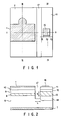
- Fig. 1 is a plan view showing an integrated optical semiconductor device.
- a stripe-shaped semiconductor laser is provided under a p-side electrode 1, and a current blocking layer having a contact layer 2 is provided at both sides of the semiconductor laser.
- the electrode 1 has a projected portion used for bonding.
- the width of the electrode is about 10 ⁇ m to 30 ⁇ m. This width can also be set to be about 200 ⁇ m to 300 ⁇ m.
- a phototransistor photodetector
- n-side electrode 16 of the phototransistor and a contact layer 11 of the n-side electrode 16 are shown.
- Fig. 2 shows a sectional view taken along a line II - II of Fig. 1.
- the semiconductor laser provided on one major surface of a semiconductor substrate 6 includes an active layer 8, a clad layer 9, and a contact layer 10 successively disposed from the lower portion, and the electrode 1 is in contact with the contact layer 10.
- the phototransistor includes a p-type InP layer 14, a light absorption layer 13, an n-type InP layer 12, the contact layer 11, and the electrode 16 successively located from the lower portion.
- a common electrode 7 for the semiconductor laser and the phototransistor is provided on the other major surface of the semiconductor substrate 6.
- the distance between the electrode 7 and the electrode 1, i.e., the thickness of the optical semiconductor device, is about 100 ⁇ m.
- the thickness of the semiconductor laser provided on the semiconductor substrate 6 is about 4 to 5 ⁇ m, and the thickness of the phototransistor is 5 to 6 ⁇ m.
- the thickness of the active layer 8 of the semiconductor laser is about 0.1 ⁇ m, and the thickness of the light absorption layer 13 of the phototransistor is about 2 to 3 ⁇ m in the embodiment. Since the common electrode 7 is formed on the substrate 6, the manufacturing steps of the optical semiconductor device become easy as compared with those of the conventional optical semiconductor device in which electrodes are separately provided to every elements.
- the current blocking layer and the photodetector in the first embodiment are provided by a multilayer semiconductor film having the same structure, and the multilayer semiconductor film has a p-i-n structure. This structure does not include the contact layer of the electrode.
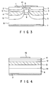
- Fig. 3 shows a sectional view taken along a line III - III of Fig. 1.
- the current blocking layer consists of the same multilayer semiconductor film as to that of the phototransistor, and the current blocking layer has a high-resistance i-type InGaAsP layer 4.
- a light component spontaneously emitted from the active layer leaks to the blocking layer, the amount of the light component is very small, and the light component is reflected by the p-type InP layer of the current blocking layer. For this reason, the absorption of the light component in the i-type layer can be neglected.
- the current blocking layer is provided by a multilayer film that includes a p-type InP layer 5, the i-type InGaAsP layer 4, an n-type InP layer 3, and the n-type InGaAsP contact layer 2.
- the semiconductor laser is provided by the nondoped InGaAsP active layer 8, the p-type InP clad layer 9, and the p-type InGaAsP contact layer 10 on which the Au-Zn electrode 1 is provided.
- the width of the active layer 8 is 1 to 1.5 ⁇ m, and the width of the electrode is 20 to 30 ⁇ m.
- Fig. 4 shows a sectional view taken along a line IV - IV of Fig. 1.
- the phototransistor is obtained by forming the p-type InP layer 14, the i-type InGaAsP light absorption layer 13, the n-type InP layer 12, and the n-type InGaAsP contact layer 11 on the n-type InP substrate 6 having the n-side electrode 7, and the electrode 16 is formed on the contact layer 11.
- the semiconductor laser is separated from the phototransistor by the groove 17 formed by dry etching such as RIE. Since the optical semiconductor device including the semiconductor laser described above can be formed by the same process as that of a conventional buried semiconductor laser, it can be mass-produced.
- the phototransistor since the phototransistor has the photosensitivity of several tens to several hundreds times as compared to a photodiode, functions of monitoring and controlling the semiconductor laser can be greatly improved.
- the electrodes can be formed by a simple process, and the device structure is not complicated, thereby improving workability of wire bonding and the like.
- the n-type InP substrate 6 is used as a semiconductor substrate.
- the nondoped InGaAsP active layer 8, the p-type clad layer 9, and the p-type InGaAs contact layer 10 are sequentially grown on the entire surface of the n-type InP substrate 6 to provide a multilayer film.
- an insulating film (not shown) such as an SiO 2 film and an Si 3 N 4 film is formed on the surface of the multilayer film.
- the surface of the multilayer film is covered with the insulating film in such a manner that the width of the active layer 8 of the semiconductor laser becomes about 1 to 1.5 ⁇ m.
- the multilayer film which is not covered with the insulating film, is selectively etched by chemical etching to provide the stripe-shaped semiconductor laser.
- the thickness of the peripheral portion thereof is decreased.
- the p-type InP layer, the i-type InGaAsP layer, the n-type InP layer, and the n-type InGaAsP layer are sequentially grown on the chemically etched substrate surface to provide the current blocking layer and the phototransistor.
- the groove 17 is formed by dry etching such as RIE to separate the current blocking layer from the phototransistor.
- the current blocking layer consisting of the p-type InP layer 5, the i-type InGaAsP layer 4, the n-type InP layer 3 and the n-type InGaAsP layer 2, and the phototransistor, consisting of the p-type InP layer 14, the i-type InGaAsP layer 13, the n-type InP layer 12 and the n-type InGaAs layer 11, are provided at the same time.
- the electrode 1 consisting of e.g., Au-Zn is formed on the p-type InGaAsP contact layer 10 of the semiconductor laser by electron beam evaporation techniques or sputtering techniques, and the electrode 16 consisting of, e.g., Au-Ge, is formed on the n-type InGaAsP contact layer 11 by the sputtering.
- the electrode 7 consisting of, e.g., Au-Ge, is formed on the opposite surface of the substrate.
- the InP semiconductor substrate is employed, and the InGaAsP semiconductor is used for the i-type layer.
- the present invention is not limited to these materials.
- a GaAs semiconductor substrate can be used.
- GaAlAs, InGaAlP, or GaAlP semiconductors can be used as the i-type layer.
- oscillation light emitted from a semiconductor laser has an energy somewhat lower than that of the band gap energy.
- the band gap can be easily changed by varying the composition ratio. Therefore, when the composition ratio y of the light absorption layer 13 is controlled within a range of 0 to 1 to have an energy gap lower than that of the active layer 8 of the semiconductor laser, the absorption sensitivity of the phototransistor can be increased.
- the composition ratio y of the light absorption layer 13 may be made higher than that of the active layer 8.
- the composition ratio y of the light absorption layer is controlled within a range of 0.55 to 0.8.
- the composition ratio y is increased, the absorption coefficient is increased, but a degree of the light absorption layer 13 which contributes to a photocurrent is decreased due to an increase in absorption and recombination at the end surface of the light absorption layer 13 of the phototransistor. Therefore, the composition ratio y of the light absorption layer 13 is given by 0.8 or less so that a light transmission length becomes about 50 ⁇ m to 500 ⁇ m.
- the carrier concentration of the light absorption layer 13 is controlled to about 2 x 10 16 cm -3 or less.
- the light absorption layer 13 has a light detection surface for receiving light from the semiconductor laser, and the light detection surface is opposed to the active layer of the semiconductor laser, i.e., the i-type layer 8, through the groove 17.
- the thickness of the light absorption layer 13 is preferably given by about 0.1 to 5.0 ⁇ m if the light detection surface receives the light within this range. Therefore, the light reception sensitivity of the phototransistor can be increased to ten times that of a conventional phototransistor. In addition, generation of a dark current can be reduced by rendering an upper limit to the band gap energy.
- the wavelength is given by 1.3 ⁇ m, 1.55 ⁇ m or other wavelength values may be used.
- a reverse bias voltage is applied to the phototransistor, a dark current of, e.g., several ⁇ A, is generated by a leakage current even if no optical signal is applied, thereby reducing the S/N ratio.
- the leakage current at the end surface of the phototransistor is comparatively large. Therefore, in order to decrease the applied voltage in the end surface, one edge of the n-side electrode 16 is spaced apart from one edge of the phototransistor to satisfy a condition of l 3 ⁇ l 1 . That is, as shown in Fig.
- the distance l 3 between the edge of the phototransistor and the edge of the n-side electrode 16 is longer than the distance l 1 between the other edge of the phototransistor opposed to the groove 17 and the other edge of the n-side electrode 16.
- This arrangement is provided because the amount of light absorption is increased at the end surface of the phototransistor opposed to the l 1 side. Therefore, a dark current generated by the phototransistor can be greatly decreased to, e.g., about several tens nA or less.
- the second embodiment of the present invention will be described below with reference to Fig. 5.
- the figure is a plan view showing an optical semiconductor device.
- a stripe-shaped active layer of a semiconductor laser for generating a laser beam is provided under the electrode 1 in parallel therewith. Therefore, the laser beam is emitted in the direction of a photodetector along an optical axis (shown in Fig. 5) that is in parallel with the electrode 1.
- the laser beam is perpendicularly incident to the photodetector, i.e., when the optical axis is perpendicular to the photodetector, the incident laser beam is reflected to increase the reflection rate returned to the laser active layer. Therefore, in order to reduce the return luminous energy, the laser beam is inclined at ⁇ degrees in the embodiment.
- the most efficient angle ⁇ for minimizing the return luminous energy is about 5 to 20 degrees.
- a semiconductor laser of the embodiment has the same structure as that of the first embodiment (Fig. 2).
- a photodetector of the third embodiment has an n-i-p-n structure, unlike the photodetector of the first embodiment.
- the multilayer semiconductor film of the n-i-p-n structure consists of an i-type InGaAsP light absorption layer 13, a p-type InP layer 14, an n-type InP layer 12, and an n-type InGaAsP contact layer 11, on which an electrode 16 is provided.
- the structure is the same as that of the current blocking layer, as in the first and second embodiments.
- An active layer 8 is opposed to the light absorption layer 13 through a groove 17, and the light absorption efficiency of the light absorption layer 13 is equal to those of the first and second embodiments.
- the fourth embodiment of the present invention will be described below with reference to Figs. 7 and 8.
- the structures of semiconductor lasers in Figs. 7 and 8 are the same as that of the first embodiment (Fig. 2).
- a photodetector in Fig. 7 has an n-i-p structure unlike the photodetector in Fig. 2.
- the multilayer semiconductor film of the n-i-p structure consists of an i-type InGaAsP light absorption layer 13, a p-type InP layer 14, and a p-type InGaAsP contact layer 11 on which an electrode 16 is provided.
- the structure is the same as that of the current blocking layer, as in the first, second and third embodiments.
- An active layer 8 is opposed to the light absorption layer 13 through a groove 17, and the light absorption efficiency of the light absorption layer 13 is equal to those of the first, second, and third embodiments.
- the fourth embodiment since a voltage is applied to the photodetecor in a forward direction, a current flows easily. However, since the i-type layer has a high resistance, it may be preferable to apply a low voltage to the photodector.
- a structure in Fig. 8 is almost the same as that of Fig. 7. That is, a photodetector in Fig. 8 has an n-i-n structure.
- the multilayer semiconductor film of the n-i-n structure consists of an i-type InGaAsP light absorption layer 13, an n-type InP layer 12, and an n-type InGaAsP contact layer 11, and an electrode 16 is provided on the contact layer.
- This structure is the same as that of the current blocking layer, as in the first, second and third embodiments.
- the photodetector having the same structure as that of current blocking layer is provided on the same substrate, it is not necessary to use a complicated manufacturing process, and the light absorbing efficiency of the photodetector can be greatly improved.
- the semiconductor laser and the photodetector can be simultaneously formed on the substrate, the optical semiconductor device can be excellently manufactured.
Description
- The present invention relates to an integrated optical semiconductor device used in optical fiber communication or optical information processing.
- In optical fiber communication or optical information processing, a light source such as a semiconductor laser has been generally used. However, in order to establish a desired information system, the phase and frequency of light emitted from the semiconductor laser must be controlled with high precision. For this reason, an optical circuit is formed on a substrate by an optical waveguide, and an optical signal must be processed, or a semiconductor optical waveguide and a photodetector must be integrated. In addition, it has been known that a photodiode is arranged at a position opposite to the radiation direction of the semiconductor laser to control or monitor the operation of the semiconductor laser. In a conventional technique, a semiconductor laser and a photodiode are independently provided, and they are fixed on a base to be opposed to each other.
- In recent years, as shown in GB-A-2 120 457, an optical semiconductor device integrated by forming a laser diode and a photodiode on the same semiconductor substrate has been proposed to obtain the most advanced functions, mass-production, and low cost. The integrated optical semiconductor device, as shown in Fig. 9, includes a semiconductor laser and a photodiode formed on an
insulating semiconductor substrate 25. The semiconductor laser consists of an n-typeInP clad layer 24, an InGaAsPactive layer 23, a p-typeInP clad layer 22, a p-typeInGaAsP contact layer 21, a p-side electrode 20, and an n-side electrode 26, and the photodiode consists of anInGaAsP layer 30 serving as an light absorption layer, an n-type InP layer 31, a p-type InP layer 29, a p-typeInGaAsP contact layer 28, an n-side electrode 32, and a p-side electrode 27. Since this photodiode is formed in the same process as that of the semiconductor laser, the composition of the photodiode is the same as that of the semiconductor laser. A positive potential and a negative potential are applied to the n-side electrode 32 and the p-side electrode 27 in the photodiode, respectively. For operating the semiconductor laser, a positive potential and a negative potential are applied to the p-side electrode 20 and the n-side electrode 26, respectively, to inject carriers to theactive layer 23. The semiconductor laser and the photodiode are separated from each other by a groove 33 formed by a dry etching technique such as RIE. The photodiode serving as a photodetector, as described above, is made as follows. That is, the semiconductor layers for providing the semiconductor laser are formed on thesemiconductor substrate 25 and etched down to thesubstrate 25 to form the groove 33. A part of the semiconductor layers separated by the groove 33 is then used as the photodiode. The photodiode, therefore, has the same structure as that of the semiconductor laser. In the semiconductor laser, the multilayer film including theactive layer 23 and the clad layers is formed to provide a stripe-shaped structure, and a current blocking layer is grown on the substrate at both sides of the stripe-shaped structure in parellel with an optical axis. In order to provide the current blocking layer, after the multilayer film is provided, the stripe-shaped active region and the surface of the photodiode are covered with an insulating film such as an SiO2 film or an Si3N4 film. Thereafter, the multilayer film is selectively removed to expose thesubstrate 25. Semiconductor layers are grown on the exposedsemiconductor substrate 25 to form a current blocking layer. Finally, the electrodes are provided to complete the integrated semiconductor device. However, with the above arrangement, since theabsorption layer 30 of the photodiode has the same composition as that of theactive layer 23 of the semiconductor laser, it has a small absorption coefficient of the laser beam, and the photodiode having a desired sensitivity cannot be obtained. In addition, since the thickness of theabsorption layer 30 has the same thickness as that of theactive layer 23, and is thin i.e., about 0.1 µm, it cannot sufficiently receive the laser beam emitted from the semiconductor laser. Furthermore, since theinsulating substrate 25 is used, the electrodes cannot be easily provided because they must be separately provided for elements on the substrate. Therefore, with the above arrangement, an optical semiconductor device having the most advanced functions, mass production, low cost cannot be obtained. - It is, therefore, an object of the present invention to provide an improved optical semiconductor device including a semiconductor laser and a phototransistor which are integrated without using an insulating substrate.
- It is another object of the present invention to provide an optical semiconductor device including a phototransistor having an improved light detection performance.
- It is still another object of the present invention to provide an integrated optical semiconductor device capable of providing a current blocking layer of a semiconductor laser and a phototransistor on the same substrae by the same process.
- According to an aspect of the present invention, there is provided an optical semiconductor device, which comprises a semiconductor substrate, a semiconductor laser, provided on the semiconductor substrate, including a stripe-shaped structure having an active layer, a current blocking layer provided on the semiconductor substrate so as to bury the semiconductor laser, a photodetector, provided on the semiconductor substrate, having the same thickness and composition as those of the current blocking layer, and a groove provided in the semiconductor substrate to define an emitting end surface of the semiconductor laser and a light detection surface of the photodetector opposed to each other.
- This invention can be more fully understood from the following detailed description when taken in conjunction with the accompanying drawings, in which:
- Fig. 1 is a plan view showing an optical semiconductor device according to a first embodiment of the present invention;
- Fig. 2 is a sectional view showing the optical semiconductor device taken along a line II - II in Fig. 1;
- Fig. 3 is a sectional view showing the optical semiconductor device taken along a line III - III in Fig. 1;
- Fig. 4 is a sectional view showing the optical semiconductor device taken along a line IV - IV in Fig. 1;
- Fig. 5 is a plan view showing an optical semiconductor device according to a second embodiment of a present invention;
- Fig. 6 is a sectional view showing an optical semiconductor device according to a third embodiment of the present invention;
- Figs. 7 and 8 are sectional views showing an optical semiconductor device according to a fourth embodiment of the present invention; and
- Fig. 9 is a sectional view showing a conventional optical semiconductor device.
- Embodiments of the present invention will be described below with reference to the accompanying drawings.
- Note that the same reference numerals denote the same parts in all drawings.
- The first embodiment will be described below with reference to Figs. 1 to 4. Fig. 1 is a plan view showing an integrated optical semiconductor device. In the integrated optical semiconductor device, a stripe-shaped semiconductor laser is provided under a p-
side electrode 1, and a current blocking layer having acontact layer 2 is provided at both sides of the semiconductor laser. Theelectrode 1 has a projected portion used for bonding. The width of the electrode is about 10 µm to 30 µm. This width can also be set to be about 200 µm to 300 µm. A phototransistor (photodetector) is provided so as to be opposed to the stripe-shaped semiconductor laser and the current blocking layer through agroove 17. In Fig. 1, an n-side electrode 16 of the phototransistor and acontact layer 11 of the n-side electrode 16 are shown. Fig. 2 shows a sectional view taken along a line II - II of Fig. 1. The semiconductor laser provided on one major surface of asemiconductor substrate 6 includes anactive layer 8, aclad layer 9, and acontact layer 10 successively disposed from the lower portion, and theelectrode 1 is in contact with thecontact layer 10. On the contrary, the phototransistor includes a p-type InP layer 14, alight absorption layer 13, an n-type InP layer 12, thecontact layer 11, and theelectrode 16 successively located from the lower portion. Acommon electrode 7 for the semiconductor laser and the phototransistor is provided on the other major surface of thesemiconductor substrate 6. The distance between theelectrode 7 and theelectrode 1, i.e., the thickness of the optical semiconductor device, is about 100 µm. The thickness of the semiconductor laser provided on thesemiconductor substrate 6 is about 4 to 5 µm, and the thickness of the phototransistor is 5 to 6 µm. The thickness of theactive layer 8 of the semiconductor laser is about 0.1 µm, and the thickness of thelight absorption layer 13 of the phototransistor is about 2 to 3 µm in the embodiment. Since thecommon electrode 7 is formed on thesubstrate 6, the manufacturing steps of the optical semiconductor device become easy as compared with those of the conventional optical semiconductor device in which electrodes are separately provided to every elements. The current blocking layer and the photodetector in the first embodiment are provided by a multilayer semiconductor film having the same structure, and the multilayer semiconductor film has a p-i-n structure. This structure does not include the contact layer of the electrode. - Fig. 3 shows a sectional view taken along a line III - III of Fig. 1. The current blocking layer consists of the same multilayer semiconductor film as to that of the phototransistor, and the current blocking layer has a high-resistance i-
type InGaAsP layer 4. Although a light component spontaneously emitted from the active layer leaks to the blocking layer, the amount of the light component is very small, and the light component is reflected by the p-type InP layer of the current blocking layer. For this reason, the absorption of the light component in the i-type layer can be neglected. The current blocking layer is provided by a multilayer film that includes a p-type InP layer 5, the i-type InGaAsP layer 4, an n-type InP layer 3, and the n-typeInGaAsP contact layer 2. On the contrary, the semiconductor laser is provided by the nondoped InGaAsPactive layer 8, the p-typeInP clad layer 9, and the p-typeInGaAsP contact layer 10 on which the Au-Zn electrode 1 is provided. The width of theactive layer 8 is 1 to 1.5 µm, and the width of the electrode is 20 to 30 µm. - Fig. 4 shows a sectional view taken along a line IV - IV of Fig. 1. The phototransistor is obtained by forming the p-
type InP layer 14, the i-type InGaAsPlight absorption layer 13, the n-type InP layer 12, and the n-typeInGaAsP contact layer 11 on the n-type InP substrate 6 having the n-side electrode 7, and theelectrode 16 is formed on thecontact layer 11. The semiconductor laser is separated from the phototransistor by thegroove 17 formed by dry etching such as RIE. Since the optical semiconductor device including the semiconductor laser described above can be formed by the same process as that of a conventional buried semiconductor laser, it can be mass-produced. In addition, since the phototransistor has the photosensitivity of several tens to several hundreds times as compared to a photodiode, functions of monitoring and controlling the semiconductor laser can be greatly improved. The electrodes can be formed by a simple process, and the device structure is not complicated, thereby improving workability of wire bonding and the like. - A method of making the optical semiconductor device will be described below. The n-
type InP substrate 6 is used as a semiconductor substrate. The nondoped InGaAsPactive layer 8, the p-type cladlayer 9, and the p-typeInGaAs contact layer 10 are sequentially grown on the entire surface of the n-type InP substrate 6 to provide a multilayer film. Thereafter, an insulating film (not shown) such as an SiO2 film and an Si3N4 film is formed on the surface of the multilayer film. In this case, the surface of the multilayer film is covered with the insulating film in such a manner that the width of theactive layer 8 of the semiconductor laser becomes about 1 to 1.5 µm. Thereafter, the multilayer film, which is not covered with the insulating film, is selectively etched by chemical etching to provide the stripe-shaped semiconductor laser. At this time, since the surface of the substrate is also etched, the thickness of the peripheral portion thereof is decreased. Thereafter, the p-type InP layer, the i-type InGaAsP layer, the n-type InP layer, and the n-type InGaAsP layer are sequentially grown on the chemically etched substrate surface to provide the current blocking layer and the phototransistor. Thegroove 17 is formed by dry etching such as RIE to separate the current blocking layer from the phototransistor. By the above steps, the current blocking layer, consisting of the p-type InP layer 5, the i-type InGaAsP layer 4, the n-type InP layer 3 and the n-type InGaAsP layer 2, and the phototransistor, consisting of the p-type InP layer 14, the i-type InGaAsP layer 13, the n-type InP layer 12 and the n-type InGaAs layer 11, are provided at the same time. After the insulating film is removed from the semiconductor laser, theelectrode 1 consisting of e.g., Au-Zn is formed on the p-typeInGaAsP contact layer 10 of the semiconductor laser by electron beam evaporation techniques or sputtering techniques, and theelectrode 16 consisting of, e.g., Au-Ge, is formed on the n-typeInGaAsP contact layer 11 by the sputtering. Finally, theelectrode 7 consisting of, e.g., Au-Ge, is formed on the opposite surface of the substrate. - In the first embodiment, the InP semiconductor substrate is employed, and the InGaAsP semiconductor is used for the i-type layer. However, the present invention is not limited to these materials. For example, a GaAs semiconductor substrate can be used. In this case, GaAℓAs, InGaAℓP, or GaAℓP semiconductors can be used as the i-type layer.
- In general, oscillation light emitted from a semiconductor laser has an energy somewhat lower than that of the band gap energy. When the
light absorption layer 13 for receiving the light is composed of a composition of InxGa1-xAsyP1-y, the band gap can be easily changed by varying the composition ratio. Therefore, when the composition ratio y of thelight absorption layer 13 is controlled within a range of 0 to 1 to have an energy gap lower than that of theactive layer 8 of the semiconductor laser, the absorption sensitivity of the phototransistor can be increased. In order to obtain thelight absorption layer 13 having a band gap energy lower than that of the oscillation light emitted from the semiconductor laser, the composition ratio y of thelight absorption layer 13 may be made higher than that of theactive layer 8. In this embodiment, since the oscillation wavelength is 1.3 µm, the composition ratio y of the light absorption layer is controlled within a range of 0.55 to 0.8. As the composition ratio y is increased, the absorption coefficient is increased, but a degree of thelight absorption layer 13 which contributes to a photocurrent is decreased due to an increase in absorption and recombination at the end surface of thelight absorption layer 13 of the phototransistor. Therefore, the composition ratio y of thelight absorption layer 13 is given by 0.8 or less so that a light transmission length becomes about 50 µm to 500 µm. In addition, since thelight absorption layer 13 must have a high resistance so that a sufficient electric field is applied thereto, the carrier concentration of thelight absorption layer 13 is controlled to about 2 x 1016 cm-3 or less. Thelight absorption layer 13 has a light detection surface for receiving light from the semiconductor laser, and the light detection surface is opposed to the active layer of the semiconductor laser, i.e., the i-type layer 8, through thegroove 17. A thickness H of thelight absorption layer 13 depends on the radiation angle of laser beam and the width of thegroove 17, and the thickness H can be expressed by H = Ltan(θ/2). In this case, L represents the width of thegroove 17, and θ represents a radiation angle when the intensity of the oscillation light emitted from the semiconductor laser is a half value. Since about 60 to 70% of light emitted from theactive layer 8 can be received by the light detection surface at a radiation angle of about ±40 degrees, the thickness of thelight absorption layer 13 is preferably given by about 0.1 to 5.0 µm if the light detection surface receives the light within this range. Therefore, the light reception sensitivity of the phototransistor can be increased to ten times that of a conventional phototransistor. In addition, generation of a dark current can be reduced by rendering an upper limit to the band gap energy. In the first embodiment, although the wavelength is given by 1.3 µm, 1.55 µm or other wavelength values may be used. - In addition, although a reverse bias voltage is applied to the phototransistor, a dark current of, e.g., several µA, is generated by a leakage current even if no optical signal is applied, thereby reducing the S/N ratio. In the first embodiment, the leakage current at the end surface of the phototransistor is comparatively large. Therefore, in order to decrease the applied voltage in the end surface, one edge of the n-
side electrode 16 is spaced apart from one edge of the phototransistor to satisfy a condition of ℓ3 ≧ ℓ1. That is, as shown in Fig. 1, the distance ℓ3 between the edge of the phototransistor and the edge of the n-side electrode 16 is longer than the distance ℓ1 between the other edge of the phototransistor opposed to thegroove 17 and the other edge of the n-side electrode 16. This arrangement is provided because the amount of light absorption is increased at the end surface of the phototransistor opposed to the ℓ1 side. Therefore, a dark current generated by the phototransistor can be greatly decreased to, e.g., about several tens nA or less. - The second embodiment of the present invention will be described below with reference to Fig. 5. The figure is a plan view showing an optical semiconductor device. A stripe-shaped active layer of a semiconductor laser for generating a laser beam is provided under the
electrode 1 in parallel therewith. Therefore, the laser beam is emitted in the direction of a photodetector along an optical axis (shown in Fig. 5) that is in parallel with theelectrode 1. However, when the laser beam is perpendicularly incident to the photodetector, i.e., when the optical axis is perpendicular to the photodetector, the incident laser beam is reflected to increase the reflection rate returned to the laser active layer. Therefore, in order to reduce the return luminous energy, the laser beam is inclined at ω degrees in the embodiment. The most efficient angle φ for minimizing the return luminous energy is about 5 to 20 degrees. - The third embodiment of the present invention will be described below with reference to Fig. 6. A semiconductor laser of the embodiment has the same structure as that of the first embodiment (Fig. 2). A photodetector of the third embodiment has an n-i-p-n structure, unlike the photodetector of the first embodiment. The multilayer semiconductor film of the n-i-p-n structure consists of an i-type InGaAsP
light absorption layer 13, a p-type InP layer 14, an n-type InP layer 12, and an n-typeInGaAsP contact layer 11, on which anelectrode 16 is provided. The structure is the same as that of the current blocking layer, as in the first and second embodiments. Anactive layer 8 is opposed to thelight absorption layer 13 through agroove 17, and the light absorption efficiency of thelight absorption layer 13 is equal to those of the first and second embodiments. - The fourth embodiment of the present invention will be described below with reference to Figs. 7 and 8. The structures of semiconductor lasers in Figs. 7 and 8 are the same as that of the first embodiment (Fig. 2). A photodetector in Fig. 7 has an n-i-p structure unlike the photodetector in Fig. 2. The multilayer semiconductor film of the n-i-p structure consists of an i-type InGaAsP
light absorption layer 13, a p-type InP layer 14, and a p-typeInGaAsP contact layer 11 on which anelectrode 16 is provided. The structure is the same as that of the current blocking layer, as in the first, second and third embodiments. Anactive layer 8 is opposed to thelight absorption layer 13 through agroove 17, and the light absorption efficiency of thelight absorption layer 13 is equal to those of the first, second, and third embodiments. In the fourth embodiment, since a voltage is applied to the photodetecor in a forward direction, a current flows easily. However, since the i-type layer has a high resistance, it may be preferable to apply a low voltage to the photodector. A structure in Fig. 8 is almost the same as that of Fig. 7. That is, a photodetector in Fig. 8 has an n-i-n structure. The multilayer semiconductor film of the n-i-n structure consists of an i-type InGaAsPlight absorption layer 13, an n-type InP layer 12, and an n-typeInGaAsP contact layer 11, and anelectrode 16 is provided on the contact layer. This structure is the same as that of the current blocking layer, as in the first, second and third embodiments. - As described above, in the optical semiconductor device according to the present invention, since the photodetector having the same structure as that of current blocking layer is provided on the same substrate, it is not necessary to use a complicated manufacturing process, and the light absorbing efficiency of the photodetector can be greatly improved. In addition, since the semiconductor laser and the photodetector can be simultaneously formed on the substrate, the optical semiconductor device can be excellently manufactured.
Claims (12)
- An optical semiconductor device comprising a semiconductor substrate (6), a semiconductor laser (6, 8, 9, 10) provided on the semiconductor substrate (6) and including a stripe-shaped structure having an active layer (8), a current blocking layer (5, 4, 3, 2) provided on the semiconductor substrate (6) so as to bury the semiconductor laser (6, 8, 9, 10),
a photodetector (14, 13, 12, 11) provided on the semiconductor substrate (6), and a groove (17) provided in the semiconductor substrate (6) to define an emitting end surface of the semiconductor laser and a light detection surface of the photodetector opposed to each other,
characterized in that the photodetector has the same thickness and composition as the current blocking layer (5, 4, 3, 2). - The optical semiconductor device according to claim 1,
characterized in that the current blocking layer (5, 4, 3, 2) and the photodetector (14, 13, 12, 11) include an i-type semiconductor layer (4, 13). - The optical semiconductor device according to claim 2,
characterized in that the i-type semiconductor layer (13) of the photodetector provides a light absorption layer. - The optical semiconductor device according to claim 3,
characterized in that a thickness H of the light absorption layer (13) is greater than the active layer (8). - The optical semiconductor device according to claim 1,
characterized in that a first positive electrode (1) is provided on the semiconductor laser, while a second positive electrode (16) is disposed on the photodetector. - The optical semiconductor device according to claim 1,
characterized in that a negative electrode (7) is provided on the semiconductor substrate (6) as a common electrode. - The optical semiconductor device according to claim 4,
characterized in that the thickness H of the light absorption layer (13) is given by H = L tan(θ/2) where L is a width of the groove (17), and θ is a radiation angle of a laser beam emitted from the semiconductor laser. - The optical semiconductor device according to claim 5,
characterized in that the first positive electrode (1) and the second positive electrode (16) are arranged such that a center line of the first and second positive electrodes (1, 16) corresponds to an optical axis. - The optical semiconductor device according to claim 5,
characterized in that a distance ℓ1 between the light detection surface and one side of the second positive electrode (16) is shorter than a distance ℓ3 between an end surface of the photodetector and an opposite side of the second positive electrode (16). - The optical semiconductor device according to claim 1,
characterized in that the light detection surface of the photodetector is inclined at an angle of 5 to 20 degrees with respect to the emitting end surface. - The optical semiconductor device according to claim 2,
characterized in that the i-type semiconductor layer (4, 13) has a band gap energy lower than that of the active layer (8). - The optical semiconductor device according to claim 2,
characterized in that the current blocking layer and the photodetector have a structure selected from n-p-i-n, n-i-p-n, n-i-p, and n-i-n structures.
Applications Claiming Priority (2)
| Application Number | Priority Date | Filing Date | Title |
|---|---|---|---|
| JP26048791A JP2980435B2 (en) | 1991-09-12 | 1991-09-12 | Semiconductor device |
| JP260487/91 | 1991-09-12 |
Publications (2)
| Publication Number | Publication Date |
|---|---|
| EP0532025A1 EP0532025A1 (en) | 1993-03-17 |
| EP0532025B1 true EP0532025B1 (en) | 1997-01-02 |
Family
ID=17348651
Family Applications (1)
| Application Number | Title | Priority Date | Filing Date |
|---|---|---|---|
| EP92115573A Expired - Lifetime EP0532025B1 (en) | 1991-09-12 | 1992-09-11 | Optical semiconductor device having semiconductor laser and photodetector |
Country Status (5)
| Country | Link |
|---|---|
| US (1) | US5281829A (en) |
| EP (1) | EP0532025B1 (en) |
| JP (1) | JP2980435B2 (en) |
| KR (1) | KR960005580B1 (en) |
| DE (1) | DE69216329T2 (en) |
Families Citing this family (18)
| Publication number | Priority date | Publication date | Assignee | Title |
|---|---|---|---|---|
| JPH0669491A (en) * | 1992-08-18 | 1994-03-11 | Fujitsu Ltd | Optical transmission device |
| ATE174118T1 (en) * | 1994-01-26 | 1998-12-15 | Horst Ahlers | TEMPERATURE SENSOR |
| DE19812199C1 (en) * | 1998-03-19 | 1999-11-04 | Siemens Ag | Method for producing a semiconductor arrangement and a semiconductor arrangement comprising at least two semiconductor elements |
| US6137123A (en) * | 1999-08-17 | 2000-10-24 | Honeywell International Inc. | High gain GaN/AlGaN heterojunction phototransistor |
| KR100490921B1 (en) * | 1999-10-30 | 2005-05-19 | 충남대학교산학협력단 | Manufacturing process for pickled turnip |
| US6265237B1 (en) * | 1999-12-15 | 2001-07-24 | Lucent Technologies Inc. | In-wafer testing of DFB semiconductor lasers |
| US7009210B2 (en) * | 2000-10-06 | 2006-03-07 | Alphion Corporation | Method and apparatus for bit-rate and format insensitive performance monitoring of lightwave signals |
| US6888171B2 (en) * | 2000-12-22 | 2005-05-03 | Dallan Luming Science & Technology Group Co., Ltd. | Light emitting diode |
| KR20010025701A (en) * | 2001-01-18 | 2001-04-06 | 임준호 | Process for preparing pickel of raw cucumbers |
| GB2389957A (en) * | 2002-06-19 | 2003-12-24 | Kamelian Ltd | Automatic power control of a semiconductor optical amplifier |
| JP4134695B2 (en) * | 2002-11-21 | 2008-08-20 | 住友電気工業株式会社 | Optical module |
| KR100493089B1 (en) * | 2002-12-17 | 2005-06-02 | 삼성전자주식회사 | Integrated optical device |
| DE10345555A1 (en) | 2003-09-30 | 2005-05-04 | Osram Opto Semiconductors Gmbh | Radiation emitting and receiving semiconductor component comprises a radiation producing region having a composition which is different from a radiation absorbing region |
| KR100750506B1 (en) * | 2004-12-10 | 2007-08-20 | 한국전자통신연구원 | Surface emitting laser device included lighting sensor and the waveguide device thereof |
| JP4706970B2 (en) * | 2006-02-16 | 2011-06-22 | 古河電気工業株式会社 | Photonic crystal semiconductor optical amplifier and integrated optical semiconductor device |
| JP2009283822A (en) | 2008-05-26 | 2009-12-03 | Mitsubishi Electric Corp | Semiconductor laser and manufacturing method thereof |
| DE102009028909A1 (en) * | 2009-08-26 | 2011-03-17 | Nanoplus Gmbh Nanosystems And Technologies | Semiconductor laser with an absorber mounted on a laser mirror |
| KR102607820B1 (en) * | 2022-10-13 | 2023-11-29 | 서미수 | Method of producing fermented pickles including many kinds of vegetables and fruits |
Family Cites Families (9)
| Publication number | Priority date | Publication date | Assignee | Title |
|---|---|---|---|---|
| JPS55148482A (en) * | 1979-05-08 | 1980-11-19 | Canon Inc | Semiconductor laser device |
| JPS5831593A (en) * | 1981-08-18 | 1983-02-24 | Nec Corp | Light integrating element |
| EP0080945B1 (en) * | 1981-11-30 | 1990-05-23 | Fujitsu Limited | Optical semiconductor device |
| JPS58186986A (en) * | 1982-04-27 | 1983-11-01 | Kokusai Denshin Denwa Co Ltd <Kdd> | Distributed feedback semiconductor laser with monitor |
| JPS61140189A (en) * | 1984-12-12 | 1986-06-27 | Canon Inc | Semiconductor laser |
| JPS61183988A (en) * | 1985-02-08 | 1986-08-16 | Matsushita Electric Ind Co Ltd | Semiconductor laser device |
| JPS62145791A (en) * | 1985-12-20 | 1987-06-29 | Agency Of Ind Science & Technol | Semiconductor device |
| JPS62150795A (en) * | 1985-12-24 | 1987-07-04 | Mitsubishi Electric Corp | Structure of semiconductor optical element |
| JPS6360563A (en) * | 1986-08-29 | 1988-03-16 | Nec Corp | Optoelectronic integrated element |
-
1991
- 1991-09-12 JP JP26048791A patent/JP2980435B2/en not_active Expired - Fee Related
-
1992
- 1992-09-09 KR KR1019920016489A patent/KR960005580B1/en not_active IP Right Cessation
- 1992-09-11 US US07/944,085 patent/US5281829A/en not_active Expired - Lifetime
- 1992-09-11 DE DE69216329T patent/DE69216329T2/en not_active Expired - Fee Related
- 1992-09-11 EP EP92115573A patent/EP0532025B1/en not_active Expired - Lifetime
Also Published As
| Publication number | Publication date |
|---|---|
| KR930006990A (en) | 1993-04-22 |
| KR960005580B1 (en) | 1996-04-26 |
| US5281829A (en) | 1994-01-25 |
| DE69216329T2 (en) | 1997-05-22 |
| JP2980435B2 (en) | 1999-11-22 |
| JPH0575214A (en) | 1993-03-26 |
| EP0532025A1 (en) | 1993-03-17 |
| DE69216329D1 (en) | 1997-02-13 |
Similar Documents
| Publication | Publication Date | Title |
|---|---|---|
| EP0532025B1 (en) | Optical semiconductor device having semiconductor laser and photodetector | |
| US5825047A (en) | Optical semiconductor device | |
| US5838708A (en) | Integration of surface emitting laser and photodiode for monitoring power output of surface emitting laser | |
| JP3141847B2 (en) | Avalanche photodiode | |
| US4577209A (en) | Photodiodes having a hole extending therethrough | |
| US5130762A (en) | Integrated quantum well feedback structure | |
| JPH05235396A (en) | Semiconductor photoreceptor | |
| US5568502A (en) | Semiconductor laser device | |
| JPH04111478A (en) | Light-receiving element | |
| US5343054A (en) | Semiconductor light-detection device with recombination rates | |
| US5061977A (en) | Semiconductor photodetector device | |
| EP0260110B1 (en) | A double heterostructure light emitting diode | |
| JP2710070B2 (en) | Semiconductor light receiving element and optical semiconductor device using this semiconductor light receiving element | |
| JP3111982B2 (en) | Waveguide type semiconductor optical device | |
| US5991473A (en) | Waveguide type semiconductor photodetector | |
| US4399448A (en) | High sensitivity photon feedback photodetectors | |
| CA2033246C (en) | Optical semiconductor device | |
| US5684307A (en) | Semiconductor photodiode having the electrodes formed on the same surface | |
| JPH09135049A (en) | Integration of surface-luminescence-laser with photodiode for monitoring its power output | |
| JP3286034B2 (en) | Semiconductor light receiving element | |
| JP3272060B2 (en) | Semiconductor element | |
| JPS6218785A (en) | Semiconductor element | |
| JPS6380590A (en) | Semiconductor laser with optical output monitor | |
| JPS6133658Y2 (en) | ||
| JPH09298338A (en) | Quantum well crystalline body and semiconductor laser |
Legal Events
| Date | Code | Title | Description |
|---|---|---|---|
| PUAI | Public reference made under article 153(3) epc to a published international application that has entered the european phase |
Free format text: ORIGINAL CODE: 0009012 |
|
| 17P | Request for examination filed |
Effective date: 19920911 |
|
| AK | Designated contracting states |
Kind code of ref document: A1 Designated state(s): DE FR GB |
|
| 17Q | First examination report despatched |
Effective date: 19951120 |
|
| GRAH | Despatch of communication of intention to grant a patent |
Free format text: ORIGINAL CODE: EPIDOS IGRA |
|
| RAP1 | Party data changed (applicant data changed or rights of an application transferred) |
Owner name: KABUSHIKI KAISHA TOSHIBA |
|
| GRAH | Despatch of communication of intention to grant a patent |
Free format text: ORIGINAL CODE: EPIDOS IGRA |
|
| GRAA | (expected) grant |
Free format text: ORIGINAL CODE: 0009210 |
|
| AK | Designated contracting states |
Kind code of ref document: B1 Designated state(s): DE FR GB |
|
| REF | Corresponds to: |
Ref document number: 69216329 Country of ref document: DE Date of ref document: 19970213 |
|
| ET | Fr: translation filed | ||
| PGFP | Annual fee paid to national office [announced via postgrant information from national office to epo] |
Ref country code: GB Payment date: 19970901 Year of fee payment: 6 |
|
| PGFP | Annual fee paid to national office [announced via postgrant information from national office to epo] |
Ref country code: DE Payment date: 19970919 Year of fee payment: 6 |
|
| PLBE | No opposition filed within time limit |
Free format text: ORIGINAL CODE: 0009261 |
|
| STAA | Information on the status of an ep patent application or granted ep patent |
Free format text: STATUS: NO OPPOSITION FILED WITHIN TIME LIMIT |
|
| 26N | No opposition filed | ||
| PG25 | Lapsed in a contracting state [announced via postgrant information from national office to epo] |
Ref country code: GB Free format text: LAPSE BECAUSE OF NON-PAYMENT OF DUE FEES Effective date: 19980911 |
|
| REG | Reference to a national code |
Ref country code: FR Ref legal event code: D6 |
|
| GBPC | Gb: european patent ceased through non-payment of renewal fee |
Effective date: 19980911 |
|
| PG25 | Lapsed in a contracting state [announced via postgrant information from national office to epo] |
Ref country code: DE Free format text: LAPSE BECAUSE OF NON-PAYMENT OF DUE FEES Effective date: 19990701 |
|
| PGFP | Annual fee paid to national office [announced via postgrant information from national office to epo] |
Ref country code: FR Payment date: 20080915 Year of fee payment: 17 |
|
| REG | Reference to a national code |
Ref country code: FR Ref legal event code: ST Effective date: 20100531 |
|
| PG25 | Lapsed in a contracting state [announced via postgrant information from national office to epo] |
Ref country code: FR Free format text: LAPSE BECAUSE OF NON-PAYMENT OF DUE FEES Effective date: 20090930 |