EP0488166B1 - Prägemetallform und Verfahren zu ihrer Herstellung - Google Patents
Prägemetallform und Verfahren zu ihrer Herstellung Download PDFInfo
- Publication number
- EP0488166B1 EP0488166B1 EP91120182A EP91120182A EP0488166B1 EP 0488166 B1 EP0488166 B1 EP 0488166B1 EP 91120182 A EP91120182 A EP 91120182A EP 91120182 A EP91120182 A EP 91120182A EP 0488166 B1 EP0488166 B1 EP 0488166B1
- Authority
- EP
- European Patent Office
- Prior art keywords
- layer
- information
- conductive layer
- plating
- substrate
- Prior art date
- Legal status (The legal status is an assumption and is not a legal conclusion. Google has not performed a legal analysis and makes no representation as to the accuracy of the status listed.)
- Expired - Lifetime
Links
- 229910052751 metal Inorganic materials 0.000 title claims description 41
- 239000002184 metal Substances 0.000 title claims description 41
- 238000004049 embossing Methods 0.000 title claims description 37
- 238000004519 manufacturing process Methods 0.000 title claims description 21
- 239000000758 substrate Substances 0.000 claims description 62
- 229920002120 photoresistant polymer Polymers 0.000 claims description 35
- 230000003287 optical effect Effects 0.000 claims description 25
- 238000000034 method Methods 0.000 claims description 20
- 238000005530 etching Methods 0.000 claims description 8
- 238000002310 reflectometry Methods 0.000 claims description 6
- 238000010521 absorption reaction Methods 0.000 claims description 3
- 238000009713 electroplating Methods 0.000 claims 9
- 239000011248 coating agent Substances 0.000 claims 1
- 238000000576 coating method Methods 0.000 claims 1
- 239000010410 layer Substances 0.000 description 91
- 238000007747 plating Methods 0.000 description 31
- 239000011521 glass Substances 0.000 description 9
- 230000007547 defect Effects 0.000 description 6
- 238000007796 conventional method Methods 0.000 description 5
- 239000012790 adhesive layer Substances 0.000 description 4
- 239000008151 electrolyte solution Substances 0.000 description 4
- 239000000853 adhesive Substances 0.000 description 3
- 230000001070 adhesive effect Effects 0.000 description 3
- 230000006835 compression Effects 0.000 description 3
- 238000007906 compression Methods 0.000 description 3
- 238000002347 injection Methods 0.000 description 3
- 239000007924 injection Substances 0.000 description 3
- 238000004544 sputter deposition Methods 0.000 description 3
- CSCPPACGZOOCGX-UHFFFAOYSA-N Acetone Chemical compound CC(C)=O CSCPPACGZOOCGX-UHFFFAOYSA-N 0.000 description 2
- 230000003247 decreasing effect Effects 0.000 description 2
- 238000001312 dry etching Methods 0.000 description 2
- 230000000694 effects Effects 0.000 description 2
- 238000005868 electrolysis reaction Methods 0.000 description 2
- 239000012535 impurity Substances 0.000 description 2
- 239000000463 material Substances 0.000 description 2
- 150000002739 metals Chemical class 0.000 description 2
- 238000005498 polishing Methods 0.000 description 2
- 229910000737 Duralumin Inorganic materials 0.000 description 1
- 239000002253 acid Substances 0.000 description 1
- 229910045601 alloy Inorganic materials 0.000 description 1
- 239000000956 alloy Substances 0.000 description 1
- 230000015572 biosynthetic process Effects 0.000 description 1
- 239000000919 ceramic Substances 0.000 description 1
- 230000002349 favourable effect Effects 0.000 description 1
- 230000006870 function Effects 0.000 description 1
- 238000005304 joining Methods 0.000 description 1
- 238000000465 moulding Methods 0.000 description 1
- 239000004033 plastic Substances 0.000 description 1
- 238000006116 polymerization reaction Methods 0.000 description 1
- 238000003825 pressing Methods 0.000 description 1
- 230000010076 replication Effects 0.000 description 1
- 230000004044 response Effects 0.000 description 1
- 239000002904 solvent Substances 0.000 description 1
- 239000010935 stainless steel Substances 0.000 description 1
- 229910001220 stainless steel Inorganic materials 0.000 description 1
- 239000000126 substance Substances 0.000 description 1
- 238000001039 wet etching Methods 0.000 description 1
Images


Classifications
-
- B—PERFORMING OPERATIONS; TRANSPORTING
- B29—WORKING OF PLASTICS; WORKING OF SUBSTANCES IN A PLASTIC STATE IN GENERAL
- B29D—PRODUCING PARTICULAR ARTICLES FROM PLASTICS OR FROM SUBSTANCES IN A PLASTIC STATE
- B29D17/00—Producing carriers of records containing fine grooves or impressions, e.g. disc records for needle playback, cylinder records; Producing record discs from master stencils
- B29D17/005—Producing optically read record carriers, e.g. optical discs
-
- G—PHYSICS
- G11—INFORMATION STORAGE
- G11B—INFORMATION STORAGE BASED ON RELATIVE MOVEMENT BETWEEN RECORD CARRIER AND TRANSDUCER
- G11B7/00—Recording or reproducing by optical means, e.g. recording using a thermal beam of optical radiation by modifying optical properties or the physical structure, reproducing using an optical beam at lower power by sensing optical properties; Record carriers therefor
- G11B7/24—Record carriers characterised by shape, structure or physical properties, or by the selection of the material
- G11B7/26—Apparatus or processes specially adapted for the manufacture of record carriers
-
- Y—GENERAL TAGGING OF NEW TECHNOLOGICAL DEVELOPMENTS; GENERAL TAGGING OF CROSS-SECTIONAL TECHNOLOGIES SPANNING OVER SEVERAL SECTIONS OF THE IPC; TECHNICAL SUBJECTS COVERED BY FORMER USPC CROSS-REFERENCE ART COLLECTIONS [XRACs] AND DIGESTS
- Y10—TECHNICAL SUBJECTS COVERED BY FORMER USPC
- Y10S—TECHNICAL SUBJECTS COVERED BY FORMER USPC CROSS-REFERENCE ART COLLECTIONS [XRACs] AND DIGESTS
- Y10S425/00—Plastic article or earthenware shaping or treating: apparatus
- Y10S425/81—Sound record
Definitions
- the present invention relates to an embossing metal mold for transferring a fine concave and convex pattern of information to the surface of an optical disk substrate for recording/reproducing the information optically, and also to a manufacturing method thereof.
- optical disks Since one bit which is a unit of information signals can be stored in a size of 1 ⁇ m or less on an optical disk substrate, optical disks have been remarkably appreciated as high density and larger capacity media.
- a substrate of such an optical disk there are known three types in accordance with purposes, i.e., a substrate for an read-only optical disk, a substrate for an write once optical disk, and a substrate for an erasable optical disk.
- Such optical disk substrates are mass-produced in such a manner that a concave and convex pattern corresponding to information is transferred thereto by a stamper, on which the concave and convex pattern corresponding to information is formed, in the injection mold method, the compression mold method or the 2P (Photo-Polymerization) method.
- a conventional stamper is manufactured in the following manner: a photo resist layer 3 is formed on a glass substrate 13; a concave and convex pattern corresponding to information is formed on the photo resist layer 3 as a result of exposure to laser light 4 for recording which is modulated by information signals, and development; a master disk thus produced is then baked at 140°C; a conductive layer 1 which is a metallic layer of Ni or the like is formed on the surface of the photo resist layer 3; an Ni electric-plating layer 2 is formed on the conductive layer 1 which functions as an electrode; the layers 1, 2 and 3 are peeled from the glass substrate 13; and the photo resist layer 3 is removed (see Fig. 2).
- the thickness of the stamper used in the injection mold method and the compression mold method is concerned with the durability of the stamper with respect to a pressure of several tens tons/cm 2 , a heat cycle of 100°C to 300°C and so forth in the molding process.
- the thickness of the stamper is small, its strength for pressure is insufficient, and the durability against the pressure is accordingly inadequate.
- the thickness of the stamper is large, non-uniform internal strain is generated due to the heat cycle, thereby causing cracks in it. With such a stamper, therefore, it is impossible to produce a large number of substrates.
- the stamper preferably has a thickness of about 300 ⁇ m in general.
- the Ni electric-plating process employed for manufacturing the stamper is a method in which a master disk is placed in an electrolytic solution of Ni sulfaminate acid so as to form an Ni electric-plating layer thereon according to the electrolysis method.
- An important factor in the Ni electric-plating process is that the plating treatment is carried out under such plating conditions that no stress is generated in the Ni electric-plating layer. It is because, if any stress exists, the Ni electric-plating layer will be bent. However, if the plating treatment is repeated many times under the same conditions which will not cause any stress, the electrolytic solution will change in quality, and some stress may exist in the Ni electric-plating layer.
- the stress in the Ni electric-plating layer is larger than adhesive strength between substances existing between the glass substrate and the Ni electric-plating layer, peeling phenomena are observed between the Ni electric-plating layer and the conductive layer or between the conductive layer and the photo resist layer or between the photo resist layer and the glass substrate, or the like (in fact, most of peeling phenomena occur between the photo resist layer and the glass substrate).
- the electrolytic solution enters peeled portions of these layers. This electrolytic solution contaminates the surface of the conductive layer and that of the Ni electric-plating layer, so that pits and projections are left on the surface of the stamper. These pits and projections, which are different from those corresponding to information signals, are defects and result in errors.
- the conventional technique has a problem that it can not provide stampers as reliably and in as short turn around time as the developing industries demand.
- United States Patent Publication 4729940 discloses the manufacturing of a master for the replication of optical disks where an Ni electroless layer is formed on a substrate and a Cu layer is formed on the Ni layer and a photoresist is formed on the Cu layer. The joining of different metals - Ni layer and Cu layer - is not complete between said layers and it is hard to obtain a stamper of high quality.
- WO Patent Publication 8606203 discloses the steps of making a glass tool such as mold with featured surfaces. Glass, however, is not appropriate for pressure stampers.
- European Patent Publication 0155000 discloses a method for manufacturing an optical memory element where the substrate is also glass and thus unsuitable for a pressure stamper.
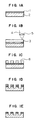
- Figs. 1A to 1E illustrate manufacturing steps of an embossing metal mold according to the present invention.
- a mirror-like substrate which provides a substrate for the embossing metal mold comprises a conductive layer 1 and an Ni electric-plating layer 2, and the mirror-like substrate is formed by Ni electric-plating after the formation of a conductive layer on a master disk on which a pattern corresponding to information is not yet formed.
- the thickness of the Ni electric-plating layer 2 is about 300 ⁇ m [Fig. 1A].
- the mirror-like substrate is coated with a positive photo resist layer 3, and the photo resist layer 3 is exposed to light of laser 4 which is modulated by information signals and focused by a lens 5.
- a concave and convex pattern corresponding to information 6 is formed in the photo resist layer 3 [Fig. 1B, Fig. 1C].
- the photo resist layer 3 is removed by a solvent such as acetone, or O 2 asher.
- a solvent such as acetone, or O 2 asher.
- portions not to be etched are coated with the photo resist layer 3 so as to perform etching of the pattern corresponding to information 6 alone. After removal of the photo resist layer 3, therefore, only pits and projections corresponding to the pattern corresponding to information 6 are formed on the surface of the stamper. Thus, the stamper of the embossing metal mold of high quality without defects can be produced.
- the embossing metal mold described above time required for manufacturing the stamper can be shortened.
- the pattern corresponding to information 6 can be formed on the conductive layer 1 of the mirror-like substrate by dry etching in several minutes, and also, it takes several minutes to remove the remaining photo resist layer 3.
- the embossing metal mold of the present invention can be produced in one hour and a half.
- Pits and projections of the pattern corresponding to information 6 are usually shaped to have a level difference of ⁇ /4n ( ⁇ : a laser wavelength of an read-out optical head, n: a refractive index of the substrate), which is about 140 nm.
- ⁇ /4n a laser wavelength of an read-out optical head
- n a refractive index of the substrate
- the thickness of the conductive layer 1 is made not less than 140 nm so that pits and projections of the pattern corresponding to information 6 will be formed in the conductive layer 1 alone.
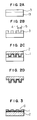
- Fig. 4A and Fig. 4B illustrate second measures for solving the above-mentioned problem.
- the embossing metal mold having projections in the conductive layer 1 and pits in the Ni electric-plating layer 2 [Fig. 4A] is further subjected to etching treatment unit1 the conductive layer 1 is removed.
- etching treatment unit1 the conductive layer 1 is removed.
- the embossing metal mold in which pits and projections of the pattern corresponding to information 6 are only formed in the Ni electric-plating layer 2 [Fig. 4B].
- optical disk substrates of high quality without defects can be mass-produced similarly.
- Fig. 5 illustrates a mirror-like substrate of low reflectivity.
- the above problem can be solved, as shown in Fig. 5, by forming the surface of the mirror-like substrate into an oxidized layer 7 by O 2 asher or the like in order to reduce the reflectivity to 50% or less after said removing process of said photoresist layer.
- O 2 asher or the like When a photo resist layer is formed on such a mirror-like substrate and exposed to light of information signals, the configuration of a pattern corresponding to information will be free from the above problem and can be worked with accuracy. The S/N of reproduced signals will be also improved.
- the auto-focus control range of the lens 5 is ⁇ 50 ⁇ m. Consequently, working of a patttern corresponding to information can be conducted accurately so long as the flatness of the surface of the mirror-like substrate is 20 ⁇ m or less. However, since the thickenss of the mirror-like substrate is as small as about 300 ⁇ m, it is difficult to maintain the flatness of 20 ⁇ m or less at the time of exposure.
- a method of maintaining the flatness of the surface of the mirror-like substrate at 20 ⁇ m or less will now be described referring to a flat mirror-like substrate of Fig. 6.
- a mirror-like substrate is secured, by an adhesive layer 9, on a supporting plate 8 which is processed accurately to have a surface flatness of 10 ⁇ m or less.
- the flatness of the surface of the mirror-like substrate can be made not more than 20 ⁇ m.
- the flatness can be improved more effectively by pressing the surface of the mirror-like substrate shown in Fig. 6 when the adhesive layer 9 is cured.
- the supporting plate 8 is made of a metal such as Al, Ni and Fe, an alloy of these metals such as stainless steel and duralumin or glass, ceramic, plastic or the like.
- the supporting plate 8 may have any thickness so long as it can be machined accurately to have a surface flatness of 10 ⁇ m or less.
- an embossing metal mold can be obtained. This peeling operation follows either the step of forming a pattern corresponding to information on a photo resist layer or the etching step of the pattern corresponding to information.
- a structure of a mirror-like substrate which facilitates peeling operation is shown in Fig. 7.
- a first Ni electric-plating layer 2 is formed on a conductive layer 1, and a peeling assist layer 10 is formed on the rear surface of the first Ni electric-plating layer 2.
- the peeling assist layer 10 is, for example, an oxidized layer by O 2 asher or the like.
- a second Ni electric-plating layer 12 is formed on the peeling assist layer 10.
- the flat mirror-like substrate is manufactured, and an embossing metal mold is obtained by peeling operation between the first and second Ni electric-plating layers 2 and 12.
- the peeling operation is easily done if the adhesive strength of the peeling assist layer 10 is made weaker than that of the adhesive layer 9. Since the second Ni electric-plating layer 12 is not used in an apparatus of manufacturing optical disk substrates, its thickness may be 300 ⁇ m, more or less.
- etching is employed in a method of forming the convexes or concaves corresponding to information instead of electric-plating which requires process time of several hours.
- time for manufacturing the stamper can be greatly shortened in comparison with the conventional technique. Therefore, many kinds of stampers can be prepared in short turn around time.
- Fig. 8 illustrates results of evaluating the roughness of conventional stampers and that of the embossing metal mold of the present invention on the basis of the output signal level of an read-out optical head.
- the output signal level is a relative intensity noise (RIN).
- Reference numeral I represents a conventional stamper with Ni electric-plating.
- Reference numeral II represents a conventional stamper having a flat plate made of a metal (Ni) which is polished with accuracy.
- Reference numeral III represents the embossing metal mold of the invention.
- the former is smaller than the latter by 3dB, and accordingly, the roughness of the mold III is smaller than that of the stamper I. It is because the mold III has the surface to which the undeveloped photo resist surface has been transferred while the stamper I has the surface to which the developed photo resist surface has been transferred. The photo resist surface is slightly melted by the development even if it is unexposed. Consequently, the roughness of the photo resist surface which is melted becomes larger than that of the undeveloped surface.
- the RIN of the stamper II is larger than that of the mold III by 21dB, and accordingly, the roughness of the stamper II is larger than that of the stamper III. It is because, even if the flat metallic (Ni) plate is polished accurately, polishing of the plate can not be performed uniformly owing to impurities which the plate material may contain, so that the plate will not be well polished in some small regions, thereby not making the roughness small.
- the roughness can be made adequately small, and consequently, optical disk substrates having high S/N can be produced.
- the concave and convex pattern corresponding to information is formed on the embossing metal mold by etching, so that the surface of the embossing metal mold will not be contaminated even if the conditions of the treatment are somewhat changed, and that the mold will have less defects, thus producing optical disk substrates of high quality.
Landscapes
- Engineering & Computer Science (AREA)
- Mechanical Engineering (AREA)
- Manufacturing & Machinery (AREA)
- Manufacturing Optical Record Carriers (AREA)
- Moulds For Moulding Plastics Or The Like (AREA)
Claims (11)
- Prägemetallstempel mit einer leitenden Schicht (1) und einer Ni-Schicht (2), bei dem die Dicke wenigstens der leitenden Schicht (1) verändert wird, um konkave und konvexe Bereiche entsprechend einer Information zu erzeugen,
dadurch gekennzeichnet,
daß die Ni-Schicht (2) eine Elektroplattier-Ni-Schicht ist und die leitende Schicht (1) aus Ni besteht. - Prägemetallstempel nach Anspruch 1,
der weiter eine oxidierte Schicht (7) auf der Oberfläche der leitenden Schicht (1) aufweist, deren Reflektivität 50 % oder weniger ist. - Prägemetallstempel nach Anspruch 1,
bei dem eine Antireflektionsschicht oder eine Absorptionsschicht auf der Oberfläche der leitenden Schicht (1) gebildet ist. - Prägemetallstempel nach Anspruch 1,
bei dem eine Trägerplatte (8) mit der hinteren Oberfläche der Elektroplattier-Ni-Schicht (2) ohne ein der Information (6) entsprechendes Muster verbunden ist. - Prägemetallstempel nach Anspruch 4,
bei dem eine zweite Elektroplattier-Ni-Schicht (12) auf der entgegengesetzten Seite der an die leitende Schicht (1) angrenzenden Elektroplattier-Ni-Schicht (2)-Oberfläche mit einer dazwischen eingefügten Abschälhilfsschicht gebildet ist. - Verfahren zur Herstellung eines Prägemetallstempels, der beim Übertragen von einer Information entsprechenden konkaven und konvexen Bereichen auf die Oberflächen optischer Scheibensubstrate verwendet wird und der eine leitende Schicht (1) und eine Ni-Schicht (2) oder eine Ni-Schicht (2) aufweist,
dadurch gekennzeichnet, daß das Verfahren die Schritte aufweist:- Herstellen einer Elektroplattier-Ni-Schicht (2) und einer leitenden Schicht (1) auf der Elektroplattier-Ni-Schicht,- Überziehen der leitenden Schicht (1) mit Photoresist (3),- Bilden der der Information entsprechenden konkaven und konvexen Bereiche auf der Photoresistschicht (3),- Übertragen der der Information entsprechenden konkaven und konvexen Bereiche auf die Oberfläche der leitenden Schicht (1) oder der Elektroplattier-Ni-Schicht (2) durch Ätzen, und- Entfernen der Photoresistschicht (3). - Herstellungsverfahren nach Anspruch 6,
bei dem die Oberfläche der leitenden Schicht (1) oxidiert wird, bis ihre Reflektivität 50 % oder weniger wird. - Herstellungsverfahren nach Anspruch 6,
bei dem eine Antireflektionsschicht oder eine Absorptionsschicht auf der Oberfläche der leitenden Schicht (1) gebildet wird. - Herstellungsverfahren nach Anspruch 6,
bei dem eine Trägerplatte (8) mit der hinteren Oberfläche des spiegelartigen Substrats ohne Informationsmuster verbunden wird und dann ein der Information (6) entsprechendes Muster auf der Oberfläche des Substrats gebildet wird. - Herstellungsverfahren nach Anspruch 9,
bei dem nach Bilden der leitenden Schicht (1) und der Elektroplattier-Ni-Schicht (2) eine Abschälhilfsschicht (10) und eine zweite Elektroplattier-Ni-Schicht (12) gebildet werden. - Stempelherstellungsverfahren nach Anspruch 6,
bei dem die leitende Schicht (1) aus Ni besteht.
Applications Claiming Priority (2)
| Application Number | Priority Date | Filing Date | Title |
|---|---|---|---|
| JP337075/90 | 1990-11-30 | ||
| JP2337075A JPH04205936A (ja) | 1990-11-30 | 1990-11-30 | 転写用成形媒体およびその製造方法 |
Publications (3)
| Publication Number | Publication Date |
|---|---|
| EP0488166A2 EP0488166A2 (de) | 1992-06-03 |
| EP0488166A3 EP0488166A3 (en) | 1992-12-23 |
| EP0488166B1 true EP0488166B1 (de) | 1997-01-29 |
Family
ID=18305200
Family Applications (1)
| Application Number | Title | Priority Date | Filing Date |
|---|---|---|---|
| EP91120182A Expired - Lifetime EP0488166B1 (de) | 1990-11-30 | 1991-11-26 | Prägemetallform und Verfahren zu ihrer Herstellung |
Country Status (4)
| Country | Link |
|---|---|
| US (1) | US5338178A (de) |
| EP (1) | EP0488166B1 (de) |
| JP (1) | JPH04205936A (de) |
| DE (1) | DE69124477T2 (de) |
Families Citing this family (13)
| Publication number | Priority date | Publication date | Assignee | Title |
|---|---|---|---|---|
| JP2868682B2 (ja) * | 1992-05-15 | 1999-03-10 | シャープ株式会社 | 光ディスク |
| FR2701152B1 (fr) * | 1993-02-03 | 1995-03-10 | Digipress Sa | Procédé de fabrication d'un disque maître pour la réalisation d'une matrice de pressage notamment de disques optiques, matrice de pressage obtenue par ce procédé et disque optique obtenu à partir de cette matrice de pressage. |
| WO1994020288A1 (en) * | 1993-03-05 | 1994-09-15 | Ict Axxicon B.V. | Mould for manufacturing disc-shaped information carriers |
| US5759457A (en) * | 1995-02-24 | 1998-06-02 | Matsushita Electric Industrial Co., Ltd. | Method for manufacturing an optical element |
| DE19642088A1 (de) * | 1996-10-12 | 1998-04-16 | Bosch Gmbh Robert | Verfahren zur Herstellung eines mikrostrukturierten Körpers, eines Gußrahmens und eines integriert-optischen Bauteils |
| DE19935558B4 (de) * | 1999-07-30 | 2010-11-25 | Nawotec Gmbh | Verfahren zur Erzeugung von Strukturen in einem Substrat im Nanometerbereich |
| DE10039208A1 (de) | 2000-08-10 | 2002-04-18 | Fraunhofer Ges Forschung | Verfahren zur Herstellung eines Werkzeugs, das zur Schaffung optisch wirksamer Oberflächenstrukturen im sub-mum Bereich einsetzbar ist, sowie ein diesbezügliches Werkzeug |
| PL217904B1 (pl) | 2000-10-05 | 2014-09-30 | Dow Global Technologies Inc | Sposób wytwarzania trwałej dyspersji polimeru w poliolu i zastosowanie trwałej dyspersji |
| JP3656591B2 (ja) | 2001-06-28 | 2005-06-08 | ソニー株式会社 | 光学記録媒体製造用スタンパの製造方法および光学記録媒体の製造方法 |
| WO2003077239A1 (en) * | 2002-03-11 | 2003-09-18 | Tdk Corporation | Processing method for photoresist master, production method for recording medium-use mater, production method for recording medium, photoresist master, recording medium-use master and recording medium |
| US7282932B2 (en) * | 2004-03-02 | 2007-10-16 | Micron Technology, Inc. | Compliant contact pin assembly, card system and methods thereof |
| TWI367821B (en) * | 2008-11-14 | 2012-07-11 | Au Optronics Corp | Mold and method for manufacturing the same |
| US10020195B2 (en) * | 2014-02-25 | 2018-07-10 | Tokyo Electron Limited | Chemical amplification methods and techniques for developable bottom anti-reflective coatings and dyed implant resists |
Family Cites Families (19)
| Publication number | Priority date | Publication date | Assignee | Title |
|---|---|---|---|---|
| US4259433A (en) * | 1976-10-22 | 1981-03-31 | Fuji Photo Film Co., Ltd. | Method for producing disk-recording plates |
| US4262875A (en) * | 1979-08-17 | 1981-04-21 | Rca Corporation | Information record stampers |
| JPS58158225A (ja) * | 1982-03-15 | 1983-09-20 | Toshiba Corp | 情報記録用基板の製造方法 |
| US4615969A (en) * | 1982-05-28 | 1986-10-07 | Energy Conversion Devices, Inc. | Method and apparatus for making a stamping master for video disk replication |
| US4650735A (en) * | 1982-10-14 | 1987-03-17 | U.S. Philips Corporation | Method of manufacturing a metal matrix and an intermediate product obtained in performing the method |
| EP0155000B1 (de) * | 1984-03-16 | 1991-08-14 | Sharp Kabushiki Kaisha | Verfahren zur Herstellung eines optischen Speicherelements |
| JPS60195749A (ja) * | 1984-03-16 | 1985-10-04 | Fujitsu Ltd | スタンパの製造方法 |
| JPS613339A (ja) * | 1984-06-18 | 1986-01-09 | Hitachi Ltd | 高密度情報記録円板複製用スタンパおよびその製造方法 |
| JPS6168746A (ja) * | 1984-09-04 | 1986-04-09 | インタ−ナショナル ビジネス マシ−ンズ コ−ポレ−ション | 光学記憶デイスクを製造するためのモ−ルド・インサ−トを形成する方法 |
| US4632898A (en) * | 1985-04-15 | 1986-12-30 | Eastman Kodak Company | Process for fabricating glass tooling |
| US4619804A (en) * | 1985-04-15 | 1986-10-28 | Eastman Kodak Company | Fabricating optical record media |
| JPH0648545B2 (ja) * | 1986-01-21 | 1994-06-22 | 共同印刷株式会社 | プリフォーマッティング用ピットのパターンを持った光記録媒体及びその製造方法 |
| US4729940A (en) * | 1986-05-16 | 1988-03-08 | Cbs Inc. | Method of manufacturing master for optical information carrier |
| JP2658023B2 (ja) * | 1986-08-20 | 1997-09-30 | 松下電器産業株式会社 | 平板状情報記録担体の原盤作成方法 |
| US4876042A (en) * | 1987-12-28 | 1989-10-24 | Canon Kabushiki Kaisha | Molding processing using a reproducible molding die |
| JPH07105067B2 (ja) * | 1988-04-28 | 1995-11-13 | キヤノン株式会社 | 情報記録媒体用基板及びその製造方法 |
| US4953385A (en) * | 1988-08-22 | 1990-09-04 | Matsushita Electric Industrial Co., Ltd. | Information storage stamper and method of manufacturing disks using the same |
| JP2564638B2 (ja) * | 1988-12-30 | 1996-12-18 | 太陽誘電株式会社 | コンパクトディスクの製造方法 |
| US5051340A (en) * | 1989-06-23 | 1991-09-24 | Eastman Kodak Company | Master for optical element replication |
-
1990
- 1990-11-30 JP JP2337075A patent/JPH04205936A/ja active Pending
-
1991
- 1991-11-26 DE DE69124477T patent/DE69124477T2/de not_active Expired - Fee Related
- 1991-11-26 EP EP91120182A patent/EP0488166B1/de not_active Expired - Lifetime
- 1991-11-27 US US07/800,455 patent/US5338178A/en not_active Expired - Fee Related
Also Published As
| Publication number | Publication date |
|---|---|
| EP0488166A3 (en) | 1992-12-23 |
| JPH04205936A (ja) | 1992-07-28 |
| EP0488166A2 (de) | 1992-06-03 |
| US5338178A (en) | 1994-08-16 |
| DE69124477D1 (de) | 1997-03-13 |
| DE69124477T2 (de) | 1997-06-26 |
Similar Documents
| Publication | Publication Date | Title |
|---|---|---|
| US6814897B2 (en) | Method for manufacturing a molding tool used for substrate molding | |
| US6207247B1 (en) | Method for manufacturing a molding tool used for sustrate molding | |
| EP1564735A2 (de) | Verfahren und Gerät zur Herstellung einer Matrize zum Formen von Strukturen von CDs und DVDs | |
| US6874262B2 (en) | Method for manufacturing master substrate used for manufacturing grooved molding substrate, method for manufacturing stamper for manufacturing grooved molding substrate, method for manufacturing grooved molding substrate, grooved molding substrate, memory medium, memory device, and computer | |
| EP0488166B1 (de) | Prägemetallform und Verfahren zu ihrer Herstellung | |
| JPH11501434A (ja) | データ記憶光ディスク用スタンパーを製造するための方法 | |
| JP2754785B2 (ja) | 高密度光ディスクの製造方法 | |
| JPS60170045A (ja) | アドレス,案内溝付光デイスク製造方法 | |
| CA2221723C (en) | Optical card | |
| JP2000280255A (ja) | 原盤の製造方法 | |
| EP0694916A2 (de) | Verfahren zur Herstellung eines Prägestempels | |
| JPH05234153A (ja) | 光ディスクの成形金型とその製造方法 | |
| KR19990030206A (ko) | 광 디스크 제조용 원반을 형성하는 방법 | |
| JPH11333885A (ja) | ファザ―・スタンパ―の大量製造方法 | |
| JP3230313B2 (ja) | 反応性イオンエッチングによるパターニング加工物の製造方法 | |
| JPH05120734A (ja) | 光デイスク及びその製造方法 | |
| KR100686146B1 (ko) | 광 기록 매체 제조방법 | |
| EP0986813B1 (de) | Halbfertigstempel | |
| JPH03156746A (ja) | 光情報記録媒体の製造方法 | |
| JPH06212458A (ja) | 反応性イオンエッチングによるパターニング 加工物の製造方法 | |
| JPH02310027A (ja) | 情報記録媒体用スタンパーの製造方法 | |
| JPH03156747A (ja) | 光情報記録媒体用スタンパーの製造方法 | |
| JPH08180468A (ja) | 光ディスク原盤 | |
| JP2000082242A (ja) | 光ディスクの製造方法及び光ディスク | |
| JPH0250330A (ja) | 光ディスク用スタンパの製造方法 |
Legal Events
| Date | Code | Title | Description |
|---|---|---|---|
| PUAI | Public reference made under article 153(3) epc to a published international application that has entered the european phase |
Free format text: ORIGINAL CODE: 0009012 |
|
| AK | Designated contracting states |
Kind code of ref document: A2 Designated state(s): DE FR GB NL |
|
| PUAL | Search report despatched |
Free format text: ORIGINAL CODE: 0009013 |
|
| AK | Designated contracting states |
Kind code of ref document: A3 Designated state(s): DE FR GB NL |
|
| 17P | Request for examination filed |
Effective date: 19921113 |
|
| 17Q | First examination report despatched |
Effective date: 19950412 |
|
| GRAG | Despatch of communication of intention to grant |
Free format text: ORIGINAL CODE: EPIDOS AGRA |
|
| GRAH | Despatch of communication of intention to grant a patent |
Free format text: ORIGINAL CODE: EPIDOS IGRA |
|
| GRAH | Despatch of communication of intention to grant a patent |
Free format text: ORIGINAL CODE: EPIDOS IGRA |
|
| GRAA | (expected) grant |
Free format text: ORIGINAL CODE: 0009210 |
|
| AK | Designated contracting states |
Kind code of ref document: B1 Designated state(s): DE FR GB NL |
|
| REF | Corresponds to: |
Ref document number: 69124477 Country of ref document: DE Date of ref document: 19970313 |
|
| ET | Fr: translation filed | ||
| PLBE | No opposition filed within time limit |
Free format text: ORIGINAL CODE: 0009261 |
|
| STAA | Information on the status of an ep patent application or granted ep patent |
Free format text: STATUS: NO OPPOSITION FILED WITHIN TIME LIMIT |
|
| 26N | No opposition filed | ||
| PGFP | Annual fee paid to national office [announced via postgrant information from national office to epo] |
Ref country code: FR Payment date: 20001025 Year of fee payment: 10 |
|
| PGFP | Annual fee paid to national office [announced via postgrant information from national office to epo] |
Ref country code: GB Payment date: 20001026 Year of fee payment: 10 |
|
| PGFP | Annual fee paid to national office [announced via postgrant information from national office to epo] |
Ref country code: NL Payment date: 20001030 Year of fee payment: 10 |
|
| PGFP | Annual fee paid to national office [announced via postgrant information from national office to epo] |
Ref country code: DE Payment date: 20001229 Year of fee payment: 10 |
|
| PG25 | Lapsed in a contracting state [announced via postgrant information from national office to epo] |
Ref country code: GB Free format text: LAPSE BECAUSE OF NON-PAYMENT OF DUE FEES Effective date: 20011126 |
|
| REG | Reference to a national code |
Ref country code: GB Ref legal event code: IF02 |
|
| PG25 | Lapsed in a contracting state [announced via postgrant information from national office to epo] |
Ref country code: NL Free format text: LAPSE BECAUSE OF NON-PAYMENT OF DUE FEES Effective date: 20020601 |
|
| PG25 | Lapsed in a contracting state [announced via postgrant information from national office to epo] |
Ref country code: DE Free format text: LAPSE BECAUSE OF NON-PAYMENT OF DUE FEES Effective date: 20020702 |
|
| GBPC | Gb: european patent ceased through non-payment of renewal fee |
Effective date: 20011126 |
|
| PG25 | Lapsed in a contracting state [announced via postgrant information from national office to epo] |
Ref country code: FR Free format text: LAPSE BECAUSE OF NON-PAYMENT OF DUE FEES Effective date: 20020730 |
|
| NLV4 | Nl: lapsed or anulled due to non-payment of the annual fee |
Effective date: 20020601 |
|
| REG | Reference to a national code |
Ref country code: FR Ref legal event code: ST |
|
| REG | Reference to a national code |
Ref country code: FR Ref legal event code: ST |