EP0485151A1 - Dispositif à ondes acoustiques de surface et procédé de fabrication - Google Patents
Dispositif à ondes acoustiques de surface et procédé de fabrication Download PDFInfo
- Publication number
- EP0485151A1 EP0485151A1 EP91310192A EP91310192A EP0485151A1 EP 0485151 A1 EP0485151 A1 EP 0485151A1 EP 91310192 A EP91310192 A EP 91310192A EP 91310192 A EP91310192 A EP 91310192A EP 0485151 A1 EP0485151 A1 EP 0485151A1
- Authority
- EP
- European Patent Office
- Prior art keywords
- metal
- acoustic
- wave device
- pattern
- package
- Prior art date
- Legal status (The legal status is an assumption and is not a legal conclusion. Google has not performed a legal analysis and makes no representation as to the accuracy of the status listed.)
- Granted
Links
Images


Classifications
-
- H—ELECTRICITY
- H03—ELECTRONIC CIRCUITRY
- H03H—IMPEDANCE NETWORKS, e.g. RESONANT CIRCUITS; RESONATORS
- H03H9/00—Networks comprising electromechanical or electro-acoustic devices; Electromechanical resonators
- H03H9/02—Details
- H03H9/05—Holders; Supports
- H03H9/10—Mounting in enclosures
- H03H9/1064—Mounting in enclosures for surface acoustic wave [SAW] devices
- H03H9/1071—Mounting in enclosures for surface acoustic wave [SAW] devices the enclosure being defined by a frame built on a substrate and a cap, the frame having no mechanical contact with the SAW device
-
- H—ELECTRICITY
- H03—ELECTRONIC CIRCUITRY
- H03H—IMPEDANCE NETWORKS, e.g. RESONANT CIRCUITS; RESONATORS
- H03H9/00—Networks comprising electromechanical or electro-acoustic devices; Electromechanical resonators
- H03H9/02—Details
- H03H9/05—Holders; Supports
- H03H9/058—Holders; Supports for surface acoustic wave devices
- H03H9/059—Holders; Supports for surface acoustic wave devices consisting of mounting pads or bumps
-
- H—ELECTRICITY
- H03—ELECTRONIC CIRCUITRY
- H03H—IMPEDANCE NETWORKS, e.g. RESONANT CIRCUITS; RESONATORS
- H03H9/00—Networks comprising electromechanical or electro-acoustic devices; Electromechanical resonators
- H03H9/02—Details
- H03H9/05—Holders; Supports
- H03H9/10—Mounting in enclosures
- H03H9/1064—Mounting in enclosures for surface acoustic wave [SAW] devices
- H03H9/1085—Mounting in enclosures for surface acoustic wave [SAW] devices the enclosure being defined by a non-uniform sealing mass covering the non-active sides of the BAW device
-
- H—ELECTRICITY
- H01—ELECTRIC ELEMENTS
- H01L—SEMICONDUCTOR DEVICES NOT COVERED BY CLASS H10
- H01L2224/00—Indexing scheme for arrangements for connecting or disconnecting semiconductor or solid-state bodies and methods related thereto as covered by H01L24/00
- H01L2224/01—Means for bonding being attached to, or being formed on, the surface to be connected, e.g. chip-to-package, die-attach, "first-level" interconnects; Manufacturing methods related thereto
- H01L2224/10—Bump connectors; Manufacturing methods related thereto
- H01L2224/15—Structure, shape, material or disposition of the bump connectors after the connecting process
- H01L2224/16—Structure, shape, material or disposition of the bump connectors after the connecting process of an individual bump connector
- H01L2224/161—Disposition
- H01L2224/16151—Disposition the bump connector connecting between a semiconductor or solid-state body and an item not being a semiconductor or solid-state body, e.g. chip-to-substrate, chip-to-passive
- H01L2224/16221—Disposition the bump connector connecting between a semiconductor or solid-state body and an item not being a semiconductor or solid-state body, e.g. chip-to-substrate, chip-to-passive the body and the item being stacked
- H01L2224/16225—Disposition the bump connector connecting between a semiconductor or solid-state body and an item not being a semiconductor or solid-state body, e.g. chip-to-substrate, chip-to-passive the body and the item being stacked the item being non-metallic, e.g. insulating substrate with or without metallisation
-
- H—ELECTRICITY
- H01—ELECTRIC ELEMENTS
- H01L—SEMICONDUCTOR DEVICES NOT COVERED BY CLASS H10
- H01L2224/00—Indexing scheme for arrangements for connecting or disconnecting semiconductor or solid-state bodies and methods related thereto as covered by H01L24/00
- H01L2224/01—Means for bonding being attached to, or being formed on, the surface to be connected, e.g. chip-to-package, die-attach, "first-level" interconnects; Manufacturing methods related thereto
- H01L2224/42—Wire connectors; Manufacturing methods related thereto
- H01L2224/47—Structure, shape, material or disposition of the wire connectors after the connecting process
- H01L2224/48—Structure, shape, material or disposition of the wire connectors after the connecting process of an individual wire connector
- H01L2224/4805—Shape
- H01L2224/4809—Loop shape
- H01L2224/48091—Arched
-
- H—ELECTRICITY
- H01—ELECTRIC ELEMENTS
- H01L—SEMICONDUCTOR DEVICES NOT COVERED BY CLASS H10
- H01L2224/00—Indexing scheme for arrangements for connecting or disconnecting semiconductor or solid-state bodies and methods related thereto as covered by H01L24/00
- H01L2224/01—Means for bonding being attached to, or being formed on, the surface to be connected, e.g. chip-to-package, die-attach, "first-level" interconnects; Manufacturing methods related thereto
- H01L2224/42—Wire connectors; Manufacturing methods related thereto
- H01L2224/47—Structure, shape, material or disposition of the wire connectors after the connecting process
- H01L2224/48—Structure, shape, material or disposition of the wire connectors after the connecting process of an individual wire connector
- H01L2224/481—Disposition
- H01L2224/48151—Connecting between a semiconductor or solid-state body and an item not being a semiconductor or solid-state body, e.g. chip-to-substrate, chip-to-passive
- H01L2224/48221—Connecting between a semiconductor or solid-state body and an item not being a semiconductor or solid-state body, e.g. chip-to-substrate, chip-to-passive the body and the item being stacked
- H01L2224/48225—Connecting between a semiconductor or solid-state body and an item not being a semiconductor or solid-state body, e.g. chip-to-substrate, chip-to-passive the body and the item being stacked the item being non-metallic, e.g. insulating substrate with or without metallisation
- H01L2224/48227—Connecting between a semiconductor or solid-state body and an item not being a semiconductor or solid-state body, e.g. chip-to-substrate, chip-to-passive the body and the item being stacked the item being non-metallic, e.g. insulating substrate with or without metallisation connecting the wire to a bond pad of the item
-
- H—ELECTRICITY
- H01—ELECTRIC ELEMENTS
- H01L—SEMICONDUCTOR DEVICES NOT COVERED BY CLASS H10
- H01L2924/00—Indexing scheme for arrangements or methods for connecting or disconnecting semiconductor or solid-state bodies as covered by H01L24/00
- H01L2924/01—Chemical elements
- H01L2924/01039—Yttrium [Y]
-
- H—ELECTRICITY
- H01—ELECTRIC ELEMENTS
- H01L—SEMICONDUCTOR DEVICES NOT COVERED BY CLASS H10
- H01L2924/00—Indexing scheme for arrangements or methods for connecting or disconnecting semiconductor or solid-state bodies as covered by H01L24/00
- H01L2924/01—Chemical elements
- H01L2924/01079—Gold [Au]
-
- H—ELECTRICITY
- H01—ELECTRIC ELEMENTS
- H01L—SEMICONDUCTOR DEVICES NOT COVERED BY CLASS H10
- H01L2924/00—Indexing scheme for arrangements or methods for connecting or disconnecting semiconductor or solid-state bodies as covered by H01L24/00
- H01L2924/30—Technical effects
- H01L2924/301—Electrical effects
- H01L2924/3011—Impedance
-
- H—ELECTRICITY
- H01—ELECTRIC ELEMENTS
- H01L—SEMICONDUCTOR DEVICES NOT COVERED BY CLASS H10
- H01L2924/00—Indexing scheme for arrangements or methods for connecting or disconnecting semiconductor or solid-state bodies as covered by H01L24/00
- H01L2924/30—Technical effects
- H01L2924/301—Electrical effects
- H01L2924/3025—Electromagnetic shielding
Definitions
- the present invention relates to a surface-acoustic-wave device adapted for high frequencies, and particularly to a surface-acoustic-wave device that has preferred performance adapted for use in the field of land mobile radio telephone systems or portable radio telephone systems and can be manufactured by simplified bonding processes to improve reliability and is suitable for mass production.
- a surface-acoustic-wave device such as a surface-acoustic-wave filter, is a three-terminal or four-terminal- type element that has an electrode for input and output formed for instance of Al on a piezoelectric substrate having a large electromechanical coupling coefficient and a relatively small temperature/frequency coefficient, such as a 36° Y-X LiTaO3 monocrystalline substrate.
- interdigital electrodes also called comb electrodes
- Typical devices have one pair of comb electrodes for input and output opposing each other.
- surface-acoustic-wave filters need a low amplitude attenuation (for example, less than or equal to 3 to 5 dB of insertion loss) and high suppression (for example, 24 to 25 dB of attenuation magnitude out of a pass band) in a wide range (for example, wider than or equal to 25 MHz of pass band at a center frequency higher than or equal to 836 MHz).
- Fig. 1 shows the electrode pattern of a conventional surface-acoustic-wave device, which illustrates the surface-acoustic-wave filter with multi-electrode construction (in this example 5 inputs and 4 outputs).
- a device element 1′ has comb electrodes 15 constituting input and output electrodes arranged alternately on a 36° Y-X LiTaO3 monocrystalline piezoelectric substrate.
- the device element is thus of a multi-electrode construction having five stages at the input side and four stages at the output side.
- the signal side electrode terminals are connected respectively to an input terminal pad 11′a and output terminal pad 11′b which are, in turn, connected to external circuits.
- reflectors may be provided at both sides for improving the characteristics.
- the reference numeral 11′c denotes grounding electrode strip pads formed electrically independent of each other.
- the reference numeral 111′ denotes a metal pattern for shielding formed surrounding the periphery of the element except for the input and output terminal pads 11′a and 11′b.
- comb electrodes terminal pad and metal pattern and so forth, are typically formed simultaneously in photo-lithographic technology by deposition of the same metal, such as Al or Al-Cu alloy.
- the illustrated comb electrode is of a so-called normal type normal construction that has an equal overlapping length of comb electrode strips. Width and number of the electrode strips on the drawing should not be considered accurate and are schematic for simplification of the drawing.
- Fig. 2 shows an example of the practical packaging of the conventional surface acoustic wave device.
- the reference numeral 1′ denotes the above-mentioned device element in multi-pole construction.
- the reference numeral 2′ denotes a package that comprises a ceramic-box-type container formed with a metallic wiring pattern 21′ on an intermediate step portion of the inner wall, for example (normally this metallic wiring pattern is formed in a pattern corresponding to that of the terminal pads of the device element 1′, and is connected to a not shown external terminal of the package).
- connection is established between the input terminal pad 11′a and the output terminal pad 11′b (including the grounding metal pattern 111′ for shielding if necessary) of the device element 1′ and the metallic wiring pattern 21′ by means of wires 7.
- the metallic lid plate 20′ is sealed and fitted to complete the surface acoustic wave device, such as the multi-electrode construction of the surface acoustic wave filter.
- surface-acoustic-wave device housing a surface-acoustic-wave device element which includes an electrode formed on a piezoelectric substrate and is mounted in a package, the surface acoustic wave device comprising a metal bump formed on a bonding pad section of the surface-acoustic-wave device element, and contact-connected with a metal pattern of the package.
- the metal pattern may be formed on a lid plate or bottom plate of the package.
- a plurality of metal bumps for grounding may be contact-connected with the metal pattern.
- a continuous raised grounding pattern may be formed along the periphery of the surface of the surface-acoustic-wave device element, on which the electrode is arranged.
- the surface-acoustic-wave device element formed of the grounding bump pattern may be contact-connected with the metal pattern, and the whole element may be coated with a resin. Furthermore, a recess or projection for positioning of the surface-acoustic-wave device element may be provided on the metal pattern.
- the invention is also directed to methods of making such a device, including lift-off methods where a resist pattern complementary to the bumps is formed on the piezoelectric substrate, deposition of one or more metal layers takes place and the resist is then lifted off, leaving the desired pattern of bumps.
- a method for producing a surface-acoustic-wave device comprising the steps of: forming a system of metal contact bumps on a piezoelectric substrate, forming corresponding metal patterns on a package for the substrate , and aligning and assembling the substrate to the package by checking the electrical connection between signal lines and a ground line.
- the metal bump is provided on the terminal pad of the surface acoustic wave device element, it is not necessary to perform wire bonding at packaging thus facilitating installation of the element. Particularly, this is effective for the multi-electrode construction type and can provide a higher reliability.
- the device since it is not necessary to provide a space for wire bonding in the package 2, the device can be made compact. Furthermore, it is simple to perform testing of the connection of the signal lines and grounding lines by means of a tester, and isolation between an input and an output can be improved by providing the grounding metal pattern.
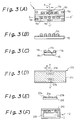
- Fig. 3 shows the first embodiment of the present invention, in (A) to (F) of this figure, a surface acoustic wave device chip, a package and packaging are schematically shown in order.
- the reference numerals 11a and 11b denote metal bumps provided on an input and output terminal pad.
- the reference numerals 11c and 11d denote metal bumps provided on a grounding terminal pad and a grounding pattern.
- the metal bumps are respectively formed of Au, for example.
- Figs. 3(B) and 3(C) are X-X′ and Y-Y′ and are cross sections of the element shown in Fig. 3(A).
- the reference numeral 15 denotes a comb electrode forming the propagation path of an surface acoustic wave.
- Fig. 3(D) shows an example of back side view of a lid plate.
- the reference numeral 20 denotes a ceramic plate formed with input and output metal patterns 21a and 21b and a grounding metal pattern 21c formed of Au layer, for example.
- the Y - Y′ cross section of the lid plate is shown in Fig. 3 (E).
- Fig. 3 (F) is a cross section of the package in the enclosed condition, in which the surface wave device 1 is die bonded on the bottom of a ceramic box shaped container 25.
- Each of the metal bumps 11 on the surface wave device 1 is made in contact with each metal pattern 21 of the lid plate 20 and interconnected therewith by depressing.
- the periphery of the lid plate 20 and the upper edge of the package 2 is bonded with a metal or resin (not shown) for completing a packaging of the element (not shown in the figure).
- the upper part of the comb (propagation area) 15 of the surface acoustic wave is spaced from the lid plate 20 by a distance equal to the height of a bump, thus producing no deterioration of performance.
- external connection terminals are omitted from the illustration.
- the connection of the element can be significantly simplified and is made compact. Also, because of no possibility of wire breakage, it may hold increased yield and reliability.
- Fig. 4 shows the pass band characteristics of an embodiment of the invention
- Fig. 5 shows the pass band characteristics of the conventional surface acoustic wave filter, which are shown for comparison with respect to the case where the identical design of the elements of 7 inputs - 6 outputs are used. There can be seen no noticeable difference. This demonstrates a remarkable advantage to be obtained by implementation of the element and the package according to the present invention, without causing any drawbacks.
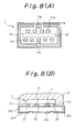
- Fig. 6 shows a second embodiment of the present invention, which is shown clearly with (partially sectioned) an assembling perspective view of the device.
- reference numeral 20′ denotes a lid plate made of a metal, 23 a frame made of ceramic, 21′ a metal pattern formed on an upper end face of the ceramic frame 23, 22 a bottom plate made of ceramic, and 24 a connection terminal to an external circuit.
- the shown embodiment is an example of how to connect the surface acoustic wave device element 1 to the bottom plate 22 via the metal bump 11, the principle and effect of which is similar to those of the foregoing first embodiment.
- Fig. 7 shows a third embodiment of the present invention, which is illustrated clearly by the (partially sectioned) assembling perspective view similar to the former figure.
- the reference numeral 20 ⁇ denotes a cap made of a metal, for example.
- the reference numeral 222 denotes a bonding material of metal or resin for sealing and bonding the cap 20 ⁇ and the bottom plate 22.
- This embodiment is essentially similar in construction to the foregoing second embodiment and can be selectively used therewith depending upon the way of use.
- Fig. 8 shows the fourth embodiment of the present invention.
- Fig. 8 (A) shows a plan view of the element
- 8 (B) shows a cross section of the device.
- the portion enclosed by the broken line represents a propagation path region of the surface acoustic wave formed by the comb electrode 15.
- the reference numeral 111 denotes a grounding bump pattern, formed with line-shaped bulged portions of Au and so forth and extending along the peripheral portion of the element except for the portion of the metal bumps 11a and 11b.
- the shielding ability of the element can be enhanced. Accordingly, when the surface-wave device 1 is connected to the bottom plate 22 provided with the metal pattern 21 (similarly for the lid plate) through the metal bump 11 and the grounding bump pattern 111, resin will not enter the inside of the element even when the outer surrounding is coated by an outer resin layer 3. Also, the characteristics will not be adversely affected even when the cap of metal and so forth is not provided.
- a metal layer may be formed on the surface-acoustic-wave device at the side opposite the operational surface for providing a further enhanced shielding effect.
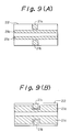
- Fig. 9 shows the fifth embodiment of the present invention.
- 9 (A) and 9 (B) show modifications of the metal pattern 21c on the lid plate (or bottom plate) of the package shown in Fig. 3.
- the grounding metal patterns 21c are separated into input side and output side. This is effective to use when better isolation between the input and output is desired.
- Fig. 10 shows the sixth embodiment of the present invention.
- 200 denotes a recess of 10 to 20 ⁇ m in depth, formed in the metal pattern 21 of the bottom plate (or lid plate 20).
- This recess 200 may be formed solely in the metal pattern 21, or as an alternative may be formed in the ceramic substrate per se located therebelow.
- Figs. 10 (A and B) show the recess 200 formed corresponding to the metal bumps 11 of the surface-wave element 1.
- Figs. 10 (C and D) show an elongated recess 200 used for the grounding metal bump. In either case, since the metal bumps engage with the recess 200, it facilitates the positioning of the element and thus make it stable.
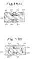
- Fig. 11 (A) shows the seventh embodiment of the present invention. Contrary to the foregoing sixth embodiment, projections 201 of a height of about 20 ⁇ m, for example, are provided on the metal pattern 21. Similar to the recess 200, the projection 201 can be formed solely with the metal pattern 21. It is of course possible to form the projection with the ceramic substrate per se located below the metal pattern. The effect is essentially equivalent to that of the case where the recess 200 of the sixth embodiment is formed.
- Fig. 11(B) shows a modification.
- Fig. 12 shows an example of a process for forming a bump in accordance with the invention, in which the principal steps are illustrated in order.
- the metal bump 11 is formed on the terminal pad of the surface device element 1, it becomes unnecessary to perform wire bonding upon packaging and thus facilitates installation. Particularly, this is effective for the multi-electrode construction type and can provide higher reliability. Also, since it is not necessary to provide a space for wire bonding in the package 2, the device can be made compact. Furthermore, it is simple to perform testing of the connection of the signal lines and grounding lines by means of a tester, and can improve isolation between input and output by providing the grounding metal pattern 21c. Therefore, the invention contributes to making the surface acoustic wave device compact and improving quality and reliability.
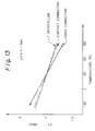
- Figure 13 is a frequency shift vs. temperature characteristic curve.
- Figure 14 is an insertion loss vs. time characteristic curve of an aging test in a 800 MHz band-pass filter.
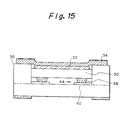
- Figure 15 is an outlined cross-sectional view showing a means for reducing contact resistance of surface-acoustic-wave devices in accordance with the present invention.
- a lid 34 is mounted to a housing in which nitrogen gas is sealed into the surface acoustic wave device 30 via a molding material 32 by means of Au-Sn sealed member 36 and a bump 38 at the bottom end of the package is contact-connected with an electrode 40.
- the contact resistance between the bump 38 and the electrode 40 is nearly equal to zero in the case of high frequency. Because contact between the electrode and the bump is maintained by virtue of an appropriate pressure of the molding member 32 or the lid 34, even if a thin insulating layer of a depth of up to 0.1 ⁇ m at the contacting surface 44 is formed, the electrostatic capacity is more than 10 pF, so in the case of a high frequency of 1GHz, impedance is no longer affected.
- a suitable load might be 200 to 500 gram weight. From experiment, it has been determined that a force of less than 200 gr. weight provides a low reliability and a contact of more than 500 gr. weight leads to destruction of a bump. Durability per bump amounts to several grams weight.
Priority Applications (2)
| Application Number | Priority Date | Filing Date | Title |
|---|---|---|---|
| EP98107844A EP0866552B1 (fr) | 1990-11-05 | 1991-11-05 | Dispositif à ondes acoustiques de surface |
| EP98107845A EP0866553B1 (fr) | 1990-11-05 | 1991-11-05 | Dispositif à ondes acoustiques de surface |
Applications Claiming Priority (2)
| Application Number | Priority Date | Filing Date | Title |
|---|---|---|---|
| JP2299472A JPH04170811A (ja) | 1990-11-05 | 1990-11-05 | 弾性表面波デバイス |
| JP299472/90 | 1990-11-05 |
Related Child Applications (2)
| Application Number | Title | Priority Date | Filing Date |
|---|---|---|---|
| EP98107844A Division EP0866552B1 (fr) | 1990-11-05 | 1991-11-05 | Dispositif à ondes acoustiques de surface |
| EP98107845A Division EP0866553B1 (fr) | 1990-11-05 | 1991-11-05 | Dispositif à ondes acoustiques de surface |
Publications (2)
| Publication Number | Publication Date |
|---|---|
| EP0485151A1 true EP0485151A1 (fr) | 1992-05-13 |
| EP0485151B1 EP0485151B1 (fr) | 1999-05-12 |
Family
ID=17873020
Family Applications (3)
| Application Number | Title | Priority Date | Filing Date |
|---|---|---|---|
| EP98107844A Expired - Lifetime EP0866552B1 (fr) | 1990-11-05 | 1991-11-05 | Dispositif à ondes acoustiques de surface |
| EP91310192A Expired - Lifetime EP0485151B1 (fr) | 1990-11-05 | 1991-11-05 | Dispositif à ondes acoustiques de surface |
| EP98107845A Expired - Lifetime EP0866553B1 (fr) | 1990-11-05 | 1991-11-05 | Dispositif à ondes acoustiques de surface |
Family Applications Before (1)
| Application Number | Title | Priority Date | Filing Date |
|---|---|---|---|
| EP98107844A Expired - Lifetime EP0866552B1 (fr) | 1990-11-05 | 1991-11-05 | Dispositif à ondes acoustiques de surface |
Family Applications After (1)
| Application Number | Title | Priority Date | Filing Date |
|---|---|---|---|
| EP98107845A Expired - Lifetime EP0866553B1 (fr) | 1990-11-05 | 1991-11-05 | Dispositif à ondes acoustiques de surface |
Country Status (4)
| Country | Link |
|---|---|
| US (1) | US5281883A (fr) |
| EP (3) | EP0866552B1 (fr) |
| JP (1) | JPH04170811A (fr) |
| DE (3) | DE69131223T2 (fr) |
Cited By (1)
| Publication number | Priority date | Publication date | Assignee | Title |
|---|---|---|---|---|
| EP0961404B1 (fr) * | 1998-05-29 | 2008-07-02 | Fujitsu Limited | Filtre à ondes acoustiques de surface avec suppression améliorée en dehors d'une bande passante |
Families Citing this family (34)
| Publication number | Priority date | Publication date | Assignee | Title |
|---|---|---|---|---|
| JPH05327394A (ja) * | 1992-05-27 | 1993-12-10 | Japan Radio Co Ltd | 弾性表面波素子のフェースダウン実装用パッケージ |
| US5459368A (en) * | 1993-08-06 | 1995-10-17 | Matsushita Electric Industrial Co., Ltd. | Surface acoustic wave device mounted module |
| JPH07154185A (ja) * | 1993-10-04 | 1995-06-16 | Nec Corp | 弾性表面波装置およびその製造方法 |
| US5939817A (en) * | 1994-09-22 | 1999-08-17 | Nippon Electric Co | Surface acoustic wave device |
| JP2872056B2 (ja) * | 1994-12-06 | 1999-03-17 | 日本電気株式会社 | 弾性表面波デバイス |
| JP3171043B2 (ja) * | 1995-01-11 | 2001-05-28 | 株式会社村田製作所 | 弾性表面波装置 |
| US5760526A (en) * | 1995-04-03 | 1998-06-02 | Motorola, Inc. | Plastic encapsulated SAW device |
| JP3308759B2 (ja) * | 1995-04-10 | 2002-07-29 | 日本電気株式会社 | 弾性表面波装置 |
| JPH08288787A (ja) * | 1995-04-10 | 1996-11-01 | Canon Inc | 弾性表面波素子装置、スペクトラム拡散通信装置およびこれを用いたシステム |
| EP0840369A4 (fr) * | 1995-06-30 | 2001-12-19 | Toshiba Kk | Composant electronique et son procede de fabrication |
| JP3306272B2 (ja) * | 1995-10-20 | 2002-07-24 | 富士通株式会社 | 弾性表面波装置 |
| JPH09232904A (ja) * | 1996-02-28 | 1997-09-05 | Oki Electric Ind Co Ltd | Sawフィルタ用セラミックパッケージ |
| EP0900477B1 (fr) | 1996-05-24 | 2001-07-18 | Epcos Ag | Composant electronique, en particulier composant a ondes acoustiques de surface (composant saw) |
| JPH10150341A (ja) * | 1996-09-19 | 1998-06-02 | Murata Mfg Co Ltd | 1ポート型弾性表面波装置 |
| JP3982876B2 (ja) * | 1997-06-30 | 2007-09-26 | 沖電気工業株式会社 | 弾性表面波装置 |
| US5969461A (en) * | 1998-04-08 | 1999-10-19 | Cts Corporation | Surface acoustic wave device package and method |
| KR100267966B1 (ko) * | 1998-07-24 | 2000-10-16 | 구자홍 | 표면 탄성파 필터의 패키지 구조 |
| EP1017169B1 (fr) * | 1998-12-29 | 2005-03-16 | Kabushiki Kaisha Toshiba | Dispositif à ondes acoustiques de surface |
| JP3351402B2 (ja) * | 1999-04-28 | 2002-11-25 | 株式会社村田製作所 | 電子素子、弾性表面波素子、それらの実装方法、電子部品または弾性表面波装置の製造方法、および、弾性表面波装置 |
| JP2000357937A (ja) * | 1999-06-17 | 2000-12-26 | Murata Mfg Co Ltd | 弾性表面波装置 |
| JP3860364B2 (ja) * | 1999-08-11 | 2006-12-20 | 富士通メディアデバイス株式会社 | 弾性表面波装置 |
| JP3386043B2 (ja) * | 2000-08-09 | 2003-03-10 | 株式会社村田製作所 | 弾性表面波デバイス |
| JP4049239B2 (ja) * | 2000-08-30 | 2008-02-20 | Tdk株式会社 | 表面弾性波素子を含む高周波モジュール部品の製造方法 |
| WO2003063561A1 (fr) * | 2002-01-24 | 2003-07-31 | Mitsubishi Materials Corporation | Carte de circuit imprime, partie electronique a structure blindee et appareil de communications radio |
| KR100455699B1 (ko) * | 2002-10-09 | 2004-11-06 | 주식회사 케이이씨 | 표면 탄성파 필터 장치 |
| JP3913700B2 (ja) | 2003-04-08 | 2007-05-09 | 富士通メディアデバイス株式会社 | 弾性表面波デバイス及びその製造方法 |
| EP1770860A1 (fr) * | 2004-03-18 | 2007-04-04 | Murata Manufacturing Co., Ltd. | Dispositif ondes acoustiques de surface |
| US20060238274A1 (en) * | 2005-04-22 | 2006-10-26 | Ycl Electronics Co., Ltd. | Surface acoustic wave device |
| JP2008306757A (ja) * | 2008-07-29 | 2008-12-18 | Hitachi Media Electoronics Co Ltd | 弾性表面波装置 |
| JP5686943B2 (ja) * | 2008-09-17 | 2015-03-18 | 太陽誘電株式会社 | 弾性波デバイス及びその製造方法 |
| JP5358724B1 (ja) | 2012-06-28 | 2013-12-04 | 太陽誘電株式会社 | 弾性波デバイス内蔵モジュール及び通信装置 |
| JP5825444B2 (ja) * | 2012-09-28 | 2015-12-02 | 株式会社村田製作所 | 弾性波装置及びその製造方法 |
| JP6106404B2 (ja) | 2012-10-30 | 2017-03-29 | 太陽誘電株式会社 | 電子部品モジュール |
| WO2017110308A1 (fr) * | 2015-12-21 | 2017-06-29 | 株式会社村田製作所 | Dispositif à ondes acoustiques |
Citations (3)
| Publication number | Priority date | Publication date | Assignee | Title |
|---|---|---|---|---|
| US4737742A (en) * | 1986-01-28 | 1988-04-12 | Alps Electric Co., Ltd. | Unit carrying surface acoustic wave devices |
| US4864470A (en) * | 1987-08-31 | 1989-09-05 | Pioneer Electronic Corporation | Mounting device for an electronic component |
| EP0367181A2 (fr) * | 1988-10-31 | 1990-05-09 | Hitachi, Ltd. | Dispositif de filtrage à ondes acoustiques de surface |
Family Cites Families (17)
| Publication number | Priority date | Publication date | Assignee | Title |
|---|---|---|---|---|
| NL7003475A (fr) * | 1969-03-28 | 1970-09-30 | ||
| US3885173A (en) * | 1973-10-09 | 1975-05-20 | Magnavox Co | Apparatus and method for coupling an acoustical surface wave device to an electronic circuit |
| JPS5216147A (en) * | 1975-07-30 | 1977-02-07 | Hitachi Ltd | Pacage method for surface elastic wave element |
| US4451753A (en) * | 1979-09-13 | 1984-05-29 | Toshio Ogawa | Piezoelectric device with surface charge shunt |
| JPS577611A (en) * | 1980-06-18 | 1982-01-14 | Fujitsu Ltd | Mounting method for elastic surface wave element |
| JPS5897840A (ja) * | 1981-12-08 | 1983-06-10 | Sharp Corp | ボンデイング方法 |
| US4545610A (en) * | 1983-11-25 | 1985-10-08 | International Business Machines Corporation | Method for forming elongated solder connections between a semiconductor device and a supporting substrate |
| US4949224A (en) * | 1985-09-20 | 1990-08-14 | Sharp Kabushiki Kaisha | Structure for mounting a semiconductor device |
| JPS62173813A (ja) * | 1986-01-28 | 1987-07-30 | Alps Electric Co Ltd | 弾性表面波素子 |
| JPS6331138A (ja) * | 1986-07-24 | 1988-02-09 | Fujitsu Ltd | 半導体装置の製造方法 |
| JPS6488546A (en) * | 1987-09-30 | 1989-04-03 | Fujitsu Ltd | Method for exposing thick film resist |
| JPS6491135A (en) * | 1987-10-02 | 1989-04-10 | Fujitsu Ltd | Method for forming thick film of photoresist |
| JPH02203612A (ja) * | 1989-02-02 | 1990-08-13 | Canon Inc | 弾性表面波素子の製造法 |
| US5006792A (en) * | 1989-03-30 | 1991-04-09 | Texas Instruments Incorporated | Flip-chip test socket adaptor and method |
| US5121299A (en) * | 1989-12-29 | 1992-06-09 | International Business Machines Corporation | Multi-level circuit structure utilizing conductive cores having conductive protrusions and cavities therein |
| JPH046841A (ja) * | 1990-04-24 | 1992-01-10 | Matsushita Electric Works Ltd | 半導体装置の実装構造 |
| US5057969A (en) * | 1990-09-07 | 1991-10-15 | International Business Machines Corporation | Thin film electronic device |
-
1990
- 1990-11-05 JP JP2299472A patent/JPH04170811A/ja active Pending
-
1991
- 1991-11-04 US US07/787,432 patent/US5281883A/en not_active Expired - Lifetime
- 1991-11-05 DE DE69131223T patent/DE69131223T2/de not_active Expired - Fee Related
- 1991-11-05 DE DE69133215T patent/DE69133215T2/de not_active Expired - Fee Related
- 1991-11-05 EP EP98107844A patent/EP0866552B1/fr not_active Expired - Lifetime
- 1991-11-05 DE DE69133231T patent/DE69133231T2/de not_active Expired - Fee Related
- 1991-11-05 EP EP91310192A patent/EP0485151B1/fr not_active Expired - Lifetime
- 1991-11-05 EP EP98107845A patent/EP0866553B1/fr not_active Expired - Lifetime
Patent Citations (3)
| Publication number | Priority date | Publication date | Assignee | Title |
|---|---|---|---|---|
| US4737742A (en) * | 1986-01-28 | 1988-04-12 | Alps Electric Co., Ltd. | Unit carrying surface acoustic wave devices |
| US4864470A (en) * | 1987-08-31 | 1989-09-05 | Pioneer Electronic Corporation | Mounting device for an electronic component |
| EP0367181A2 (fr) * | 1988-10-31 | 1990-05-09 | Hitachi, Ltd. | Dispositif de filtrage à ondes acoustiques de surface |
Non-Patent Citations (2)
| Title |
|---|
| PATENT ABSTRACTS OF JAPAN vol. 14, no. 493 (E-0995)26 October 1990 & JP-A-02 203 612 ( CANON ) 13 August 1990 * |
| PATENT ABSTRACTS OF JAPAN vol. 7, no. 200 (E-196)3 September 1983 & JP-A-58 097 840 ( SHARP ) 10 June 1983 * |
Cited By (1)
| Publication number | Priority date | Publication date | Assignee | Title |
|---|---|---|---|---|
| EP0961404B1 (fr) * | 1998-05-29 | 2008-07-02 | Fujitsu Limited | Filtre à ondes acoustiques de surface avec suppression améliorée en dehors d'une bande passante |
Also Published As
| Publication number | Publication date |
|---|---|
| EP0866553A2 (fr) | 1998-09-23 |
| EP0485151B1 (fr) | 1999-05-12 |
| EP0866552A2 (fr) | 1998-09-23 |
| DE69131223T2 (de) | 1999-09-23 |
| DE69133215T2 (de) | 2003-10-09 |
| EP0866552B1 (fr) | 2003-04-02 |
| DE69133231T2 (de) | 2003-11-13 |
| DE69133215D1 (de) | 2003-04-17 |
| JPH04170811A (ja) | 1992-06-18 |
| EP0866553B1 (fr) | 2003-03-12 |
| US5281883A (en) | 1994-01-25 |
| DE69133231D1 (de) | 2003-05-08 |
| DE69131223D1 (de) | 1999-06-17 |
| EP0866552A3 (fr) | 1999-06-30 |
| EP0866553A3 (fr) | 1999-06-30 |
Similar Documents
| Publication | Publication Date | Title |
|---|---|---|
| EP0866553B1 (fr) | Dispositif à ondes acoustiques de surface | |
| EP1296454B1 (fr) | Elément et dispositif à ondes acoustiques de surface | |
| US6919777B2 (en) | Surface acoustic wave filter device | |
| EP0637871B1 (fr) | Module sur lequel est monté un dispositif à ondes acoustiques de surface | |
| US6566981B2 (en) | Surface acoustic wave device having plural ground conductor films in the housing cavity | |
| EP2043263A1 (fr) | Dispositif à ondes acoustiques de surface pour montage à flip-chip | |
| KR100708793B1 (ko) | 필터 칩 및 필터 장치 | |
| US20010029650A1 (en) | Method of producing surface acoustic wave device | |
| KR100445569B1 (ko) | 플립-칩어셈블리에적합한전기소자의콘택을제조하기위한방법 | |
| JP3887037B2 (ja) | 弾性表面波フィルタ装置 | |
| EP1635456A2 (fr) | Dispositif à ondes acoustiques de surface et procédé de sa fabrication | |
| KR20010041451A (ko) | 탄성표면파소자와 탄성표면파장치 | |
| CN110880921B (zh) | 体声波结构、体声波装置及其制造方法 | |
| CN110663178B (zh) | 电子部件以及具备该电子部件的模块 | |
| US6946929B2 (en) | Surface acoustic wave device having connection between elements made via a conductor not on the piezoelectric substrate | |
| US6972509B2 (en) | Surface acoustic wave device method of manufacturing the same, and electronic component using the same | |
| JP3329175B2 (ja) | 弾性表面波デバイス及びその製造方法 | |
| JPH03284006A (ja) | 弾性表面波デバイス | |
| KR100333805B1 (ko) | 표면 탄성파 필터 | |
| KR100306630B1 (ko) | 복합 표면 탄성파 필터 | |
| KR100368607B1 (ko) | 반도체 패키지 | |
| KR100484078B1 (ko) | 탄성 표면파 장치 및 그 제조 방법과 이것을 이용한 전자부품 | |
| JPH1188108A (ja) | 弾性表面波装置 | |
| JP2000164744A (ja) | 表面波デバイスとそのパッケージ | |
| JP2000165193A (ja) | 弾性表面波フィルタチップおよび弾性表面波フィルタ装置 |
Legal Events
| Date | Code | Title | Description |
|---|---|---|---|
| PUAI | Public reference made under article 153(3) epc to a published international application that has entered the european phase |
Free format text: ORIGINAL CODE: 0009012 |
|
| AK | Designated contracting states |
Kind code of ref document: A1 Designated state(s): DE FR GB |
|
| 17P | Request for examination filed |
Effective date: 19920722 |
|
| 17Q | First examination report despatched |
Effective date: 19941027 |
|
| APAB | Appeal dossier modified |
Free format text: ORIGINAL CODE: EPIDOS NOAPE |
|
| APAD | Appeal reference recorded |
Free format text: ORIGINAL CODE: EPIDOS REFNE |
|
| APAB | Appeal dossier modified |
Free format text: ORIGINAL CODE: EPIDOS NOAPE |
|
| GRAG | Despatch of communication of intention to grant |
Free format text: ORIGINAL CODE: EPIDOS AGRA |
|
| GRAG | Despatch of communication of intention to grant |
Free format text: ORIGINAL CODE: EPIDOS AGRA |
|
| GRAH | Despatch of communication of intention to grant a patent |
Free format text: ORIGINAL CODE: EPIDOS IGRA |
|
| GRAH | Despatch of communication of intention to grant a patent |
Free format text: ORIGINAL CODE: EPIDOS IGRA |
|
| GRAA | (expected) grant |
Free format text: ORIGINAL CODE: 0009210 |
|
| AK | Designated contracting states |
Kind code of ref document: B1 Designated state(s): DE FR GB |
|
| REF | Corresponds to: |
Ref document number: 69131223 Country of ref document: DE Date of ref document: 19990617 |
|
| ET | Fr: translation filed | ||
| PG25 | Lapsed in a contracting state [announced via postgrant information from national office to epo] |
Ref country code: GB Free format text: LAPSE BECAUSE OF NON-PAYMENT OF DUE FEES Effective date: 19991105 |
|
| PLBE | No opposition filed within time limit |
Free format text: ORIGINAL CODE: 0009261 |
|
| STAA | Information on the status of an ep patent application or granted ep patent |
Free format text: STATUS: NO OPPOSITION FILED WITHIN TIME LIMIT |
|
| 26N | No opposition filed | ||
| GBPC | Gb: european patent ceased through non-payment of renewal fee |
Effective date: 19991105 |
|
| APAH | Appeal reference modified |
Free format text: ORIGINAL CODE: EPIDOSCREFNO |
|
| PGFP | Annual fee paid to national office [announced via postgrant information from national office to epo] |
Ref country code: DE Payment date: 20061102 Year of fee payment: 16 |
|
| PGFP | Annual fee paid to national office [announced via postgrant information from national office to epo] |
Ref country code: FR Payment date: 20061108 Year of fee payment: 16 |
|
| PG25 | Lapsed in a contracting state [announced via postgrant information from national office to epo] |
Ref country code: DE Free format text: LAPSE BECAUSE OF NON-PAYMENT OF DUE FEES Effective date: 20080603 |
|
| REG | Reference to a national code |
Ref country code: FR Ref legal event code: ST Effective date: 20080930 |
|
| PG25 | Lapsed in a contracting state [announced via postgrant information from national office to epo] |
Ref country code: FR Free format text: LAPSE BECAUSE OF NON-PAYMENT OF DUE FEES Effective date: 20071130 |