EP0481190B1 - Multiple-clock-cycle subranging analog-to-digital converter - Google Patents
Multiple-clock-cycle subranging analog-to-digital converter Download PDFInfo
- Publication number
- EP0481190B1 EP0481190B1 EP91114027A EP91114027A EP0481190B1 EP 0481190 B1 EP0481190 B1 EP 0481190B1 EP 91114027 A EP91114027 A EP 91114027A EP 91114027 A EP91114027 A EP 91114027A EP 0481190 B1 EP0481190 B1 EP 0481190B1
- Authority
- EP
- European Patent Office
- Prior art keywords
- voltage
- group
- ladder
- coarse
- fine
- Prior art date
- Legal status (The legal status is an assumption and is not a legal conclusion. Google has not performed a legal analysis and makes no representation as to the accuracy of the status listed.)
- Expired - Lifetime
Links
Images


Classifications
-
- H—ELECTRICITY
- H03—ELECTRONIC CIRCUITRY
- H03M—CODING; DECODING; CODE CONVERSION IN GENERAL
- H03M1/00—Analogue/digital conversion; Digital/analogue conversion
- H03M1/06—Continuously compensating for, or preventing, undesired influence of physical parameters
- H03M1/0617—Continuously compensating for, or preventing, undesired influence of physical parameters characterised by the use of methods or means not specific to a particular type of detrimental influence
- H03M1/0675—Continuously compensating for, or preventing, undesired influence of physical parameters characterised by the use of methods or means not specific to a particular type of detrimental influence using redundancy
- H03M1/069—Continuously compensating for, or preventing, undesired influence of physical parameters characterised by the use of methods or means not specific to a particular type of detrimental influence using redundancy by range overlap between successive stages or steps
-
- H—ELECTRICITY
- H03—ELECTRONIC CIRCUITRY
- H03M—CODING; DECODING; CODE CONVERSION IN GENERAL
- H03M1/00—Analogue/digital conversion; Digital/analogue conversion
- H03M1/12—Analogue/digital converters
- H03M1/1205—Multiplexed conversion systems
- H03M1/121—Interleaved, i.e. using multiple converters or converter parts for one channel
- H03M1/1215—Interleaved, i.e. using multiple converters or converter parts for one channel using time-division multiplexing
-
- H—ELECTRICITY
- H03—ELECTRONIC CIRCUITRY
- H03M—CODING; DECODING; CODE CONVERSION IN GENERAL
- H03M1/00—Analogue/digital conversion; Digital/analogue conversion
- H03M1/12—Analogue/digital converters
- H03M1/14—Conversion in steps with each step involving the same or a different conversion means and delivering more than one bit
- H03M1/142—Conversion in steps with each step involving the same or a different conversion means and delivering more than one bit the reference generators for the steps being arranged in a common two-dimensional array
-
- H—ELECTRICITY
- H03—ELECTRONIC CIRCUITRY
- H03M—CODING; DECODING; CODE CONVERSION IN GENERAL
- H03M1/00—Analogue/digital conversion; Digital/analogue conversion
- H03M1/12—Analogue/digital converters
- H03M1/14—Conversion in steps with each step involving the same or a different conversion means and delivering more than one bit
- H03M1/144—Conversion in steps with each step involving the same or a different conversion means and delivering more than one bit the steps being performed sequentially in a single stage, i.e. recirculation type
-
- H—ELECTRICITY
- H03—ELECTRONIC CIRCUITRY
- H03M—CODING; DECODING; CODE CONVERSION IN GENERAL
- H03M1/00—Analogue/digital conversion; Digital/analogue conversion
- H03M1/12—Analogue/digital converters
- H03M1/14—Conversion in steps with each step involving the same or a different conversion means and delivering more than one bit
- H03M1/145—Conversion in steps with each step involving the same or a different conversion means and delivering more than one bit the steps being performed sequentially in series-connected stages
- H03M1/146—Conversion in steps with each step involving the same or a different conversion means and delivering more than one bit the steps being performed sequentially in series-connected stages all stages being simultaneous converters
Definitions
- the present invention pertains to Multiple-clock-cycle subranging analog-to-digital (A/D) converters and more specifically to low error, high speed multiple-clock-cycle subranging A/D converters.
- A/D analog-to-digital
- A/D converters are critical building blocks for many digital signal processing applications.
- flash type A/D converters require a comparator for each division of the reference voltage ladder, i.e. each division representing a most significant bit (MSB) and each division representing a least significant bit (LSB) between each of the MSBs.
- subranging type A/D converters only require a comparator for each MSB and a comparator for each LSB between approximately a single pair of MSBs.
- a plurality of electronic switches are provided to switch the LSB comparators to the portion of the reference voltage ladder which most nearly compares to the unknown voltage being digitized. This substantial reduction in the number of comparators greatly reduces the chip size.
- a multiple-clock-cycle subranging type analog-to-digital converter according to the pre-characterizing portion of claim 1 is known from 1989 IEEE INTERNATIONAL SOLID-STATE CIRCUITS CONFERENCE, DIGEST OF TECHNICAL PAPERS, FIRST EDITION (CAT NO. CH2684-9), NEW YORK, NY, USA, 15-17 FEB. 1989,14-15, 273, XP000066806, Fukushima N et al 'A CMOS 40MHz 8b 105mW Two-Step ADC'.
- the invention provides a multiple-clock-cycle subranging type analog-to-digital converter as claimed in claim 1.
- A/D converter 10 includes a first group of voltage comparators 12 and an encoder 14 for determining the MSB, a second group of voltage comparators 16 and an encoder 18 for determining the LSB, a reference voltage ladder 20 and a network of electronic switches 22 connecting second group of voltage comparators 12 to reference voltage ladder 20.
- the outputs of MSB encoder 14 and LSB encoder 18 are supplied to an MSB correction circuit 24 and the output of circuit 24 is supplied with the output of LSB encoder 18 to an output buffer 26.
- Each individual voltage comparator in first and second groups of voltage comparators 12 and 16 is, preferably, a low noise voltage comparator similar to that described in a co-pending patent application entitled "Voltage Comparator With Sample Hold Circuit", filed on 5th day of July, 1990, serial number 548,529, and assigned to the same assignee.
- any of the well known voltage comparators used in the "flash” and “subranging” A/D converters can be utilized, if desired.
- a simple one-pole single-throw switch is illustrated for each of the electronic switches in network 22, to simplify the drawings, it should be understood that these switches will generally be some type of semiconductor switch, such as the well known transmission gate type of switch.
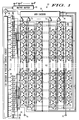
- A/D converter 10 is integrated on a single semiconductor chip generally as laid out schematically in FIG.1 with reference voltage ladder 20, switch network 22 and all of the connecting wiring distributed as illustrated.
- First group of voltage comparators 12 is connected directly to a plurality of coarse steps of reference voltage ladder 20.
- the present embodiment is illustrated as providing a six bit output signal, with three bits representing the MSB and three bits representing the LSB.
- the reference voltage ladder is divided into eight coarse steps designated 000 through 111 and each coarse step is divided into eight fine steps.
- eight fine resistors are positioned between each pair of coarse resistors (a total of 64 resistors) to form the reference ladder.
- a switching system connects the fine resistors to different points in the coarse resistor ladder.
- One of the switches of switching network 22 (a total of 128 switches in this embodiment) is connected to each end of each resistor in reference ladder 20 and to one of the voltage comparators in the second group of voltage comparators 16.
- a control input of each of the switches is connected to a control signal output of MSB encoder 14.
- An input voltage terminal 30 is adapted to have applied thereto an analog signal (unknown voltage) which it is desired to digitize.
- Terminal 30 is connected to one input of each of the voltage comparators in first group 12 and second group 16.
- a first reference voltage terminal 32 is connected to one end of reference voltage ladder 20 and a second reference voltage terminal 34 is connected to the other end of reference voltage ladder 20.
- terminal 32 will have a high potential applied thereto and terminal 34 will have a low potential applied thereto, e.g. ground.
- a plurality of control lines 36 are connected between the output of MSB encoder 14 and the control inputs of the electronic switches.
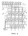
- second group of voltage comparators 16 includes 17 voltage comparators (labelled 16A through 16Q), only nine of which are illustrated in FIG.2.
- reference voltage ladder 20 has eight fine sections. or fine resistors, (A1 through A8, B1 through B8, etc.). Each fine resistor A1 through H8 has two electronic switches associated therewith, each of which has one terminal connected to opposite sides of the fine resistor (except for the five fine resistors adjacent each end of reference ladder 20) and the other terminal connected to the signal input of one of the voltage comparators 16A through 16S.
- the control lines 36 from the output of MSB encoder 14 to the control inputs of the electronic switches are labelled 36A through 36H.
- first group of voltage comparators 12 compare the unknown voltage level (analog signal) on terminal 30 to the eight coarse voltage levels provided by the reference voltage ladder 20 and signals are supplied to MSB encoder 14 indicating which voltage comparator of first group 12 has a reference voltage applied thereto (coarse step) that most nearly approximates the unknown voltage.
- MSB encoder 14 supplies this information to MSB correction circuit 24 and, on the control lines 36, to the control inputs of various electronic switches in network 22.
- the electronic switches which are energized by the control signals from MSB encoder 14 connect the second group of voltage comparators 16 to the fine steps contained within the selected coarse step and to one half of the fine steps in each coarse step adjacent to the selected coarse step.
- the voltage comparator in first group 14 corresponding to this step supplies a control voltage on control line 36C, which activates (closes) all switches connected to line 36C. From FIG.2 it can be seen that every other switch in line 20C (beginning with the first switch on the left) is connected to control line 36C. Thus, first fine resistor C1 in line 20C is connected to voltage comparator 16F, second fine resistor C2 is connected to voltage comparator 16G, etc. until last fine resistor C8 in line 20C is connected to voltage comparator 16L.
- control line 36C is connected to five switches in line 20B associated with the first five fine resistors, B1 through B5, and to five switches in line 20D associated with the last five fine resistors, D4 through D8.
- the switches in line 20B activated by control line 36C connect fine resistor B1 to voltage comparator 16E, fine resistor B2 to voltage comparator 16D, etc., until fine resistor B5 is connected to voltage comparator 16A.
- fine resistors D4 through D8 are connected to voltage comparators 16M through 16Q.
- FIG.3 a graphical representation of the coarse and fine step coverage in prior art A/D converters is illustrated.
- An six bit accuracy A/D converter is illustrated for convenience in comparison.
- the fine steps in the prior art structure extend across the selected coarse step (e.g. 100) and, additionally, for two fine steps on the lower end (110 and 111) and three fine steps on the upper end (001, 010 and 011).
- the coarse voltage comparators indicate that the unknown voltage lies between 100 and 101, because of tolerances and minor noise errors, the actual fine step could be below 100110 or above 101011.
- the fine comparators would not be able to make a comparison on the second clock cycle.
- the MSB comparison can be more than three fine steps away from the actual unknown voltage. As long as the actual signal remains at this level and the MSB portion of the A/D converter indicates a higher or lower coarse step, the output will be in error.
- the present invention includes fine voltage comparators that extend across the selected coarse step and from approximately the center of each adjacent coarse step so that no fine steps are missed, as illustrated in FIG.4. If the first group of voltage comparators 12 and MSB encoder 14 indicate that the unknown voltage supplied to terminal 30 lies between coarse steps 100 and 101, a control signal is supplied to switching network 22 which connects the second group of voltage comparators 16 to fine steps 100100 (voltage comparator 16A) through 101100 (voltage comparator 16Q). Thus, the entire range of fine steps is covered and no errors can occur because of too great a tolerance and/or noise in the MSB portion of the determination.
- FIG.5 another embodiment of the present invention is illustrated in which the entire two-clock-cycle subranging A/D converter operates nearly as fast as a one-clock-cycle flash type of A/D converter.
- components which are similar to those in FIG.1 are designated with similar numbers and a prime is added to indicate the different embodiment.
- a first group of voltage comparators 12' is connected to a reference voltage ladder 20' as described in the first embodiment.
- a second group of voltage comparators 16' is connected to reference voltage ladder 20' by switching network 22', as described in conjunction with the embodiment of FIG.1.
- a third group of voltage comparators 40' is connected to reference voltage ladder 20' by switching network 22' exactly as the second group of voltage comparators 16' is connected.
- Third group of voltage comparators 40' are connected to a second LSB encoder 42' which in turn supplies an output signal to an MSB correction circuit 24' and to an output buffer 26'.
- the timing signals supplied to the third group of voltage comparators 40' are 180 degrees out of phase with the timing signals supplied to the second group of voltage comparators 16'.
- the first and second groups of voltage comparators 12' and 16' sample the unknown voltage applied to input terminal 30' and are autozeroed by the sample.
- the first group of voltage comparators 12' determine an MSB (coarse) reading and, through encoder 14', supply control signals that connect the second group of voltage comparators 16' to the appropriate fine resistors in reference voltage ladder 20'.
- the second group of voltage comparators 16' determines the LSB reading, corrects the MSB reading in MSB correction circuit 24' (if necessary) and supplies a multiple digit output signal to output buffer 26'.
- the first and third groups of voltage comparators 12' and 40' sample the unknown voltage at input terminal 30' and are autozeroed by the second sample.
- the first group of voltage comparators 12' determines an MSB reading for the second sample and, through encoder 14', connects the third group of voltage comparators 40' to the appropriate fine resistors in reference ladder 20'.
- the third group of voltage comparators 40' determines the LSB reading for the second sample, corrects the MSB reading in MSB correction circuit 24' (if necessary) and supplies a multiple digit output signal to output buffer 26'.
- first and second groups of voltage comparators 12' and 16' sample the unknown voltage at input terminal 30' and are autozeroed by the third sample. This procedure continues, with first group of voltage comparators 12' providing an MSB output for each clock pulse and second and third groups of voltage comparators 16' and 40' alternately providing an LSB output on every clock pulse.
- the timing described herein can be accomplished very simply by supplying the same timing signals to the second and third groups of voltage comparators, 16' and 40', respectively, except that all timing signals are inverted before being applied to one of the groups of comparators 16' or 40'.
- a complete digital reading is supplied on every clock pulse (after the first clock pulse) instead of every other clock pulse as in prior art two-clock-cycle subranging A/D converters.
- a reference voltage ladder 50 which includes eight coarse steps and eight fine steps between each coarse step.
- the reference voltage ladder is actually a resistance ladder formed by providing a fine resistor for each fine step thereof, with all of the resistors being connected in a series combination and first and second reference voltages, 52 and 54, connected to opposite ends thereof.
- a first group of voltage comparators 56 is connected to reference voltage ladder 50, one comparator of the group being connected to each coarse step thereof.
- a switching network 60 is connected to reference voltage ladder 50 and to a second group of voltage comparators 62 and a third group of voltage comparators 64.
- second and third groups of voltage comparators 62 and 64 each include a number of comparators equal to twice the number of fine steps in each of the coarse steps of reference voltage ladder 50, to provide the increased accuracy described in conjunction with the embodiment of FIG.1.
- switching network 60 alternately connects either the second or the third group of voltage comparators, 62 or 64, to fine steps of reference voltage ladder 50 which are selected by an MSB encoder 66, as described in conjunction with the embodiment of FIG.5.
- An LSB encoder 70 is connected to receive output signals from second and third groups of voltage comparators 62 and 64.
- LSB encoder 70 is illustrated as a single encoder which provides the functions of two encoders, rather than illustrating two encoders as shown in FIG.5, since a single encoder might be utilized for the dual purpose and simply switched (multiplexed) between groups of voltage comparators.
- the outputs of MSB encoder 66 and LSB encoder(s) 70 are supplied to an upper bit correction circuit 72 and, ultimately, to an output buffer 74.
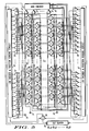
- All of the resistors of reference voltage ladder 50 are positioned on a semiconductor chip in a first common area, basically as shown in FIG.6, rather than being intermixed with switching network 60 as shown in FIG.5. Also, switching network 60 is positioned in a second common area on the semiconductor chip.
- First group of voltage comparators 56 is positioned in a third common area on a different side of reference voltage ladder 50 (the first common area) from switching network 60 (the second common area).
- Second and third groups of voltage comparators 62 and 64 are positioned in a fourth common area on a different side of switching network 60 (the second common area) from reference voltage ladder 50 (the first common area).
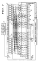
- FIG.7 another embodiment of the present invention is illustrated.
- components which are similar to those in FIG.6 are designated with similar numbers and a prime is added to indicate the different embodiment.
- the resistance ladder forming reference voltage ladder 50' is formed with a coarse section 80' connected between first and second reference voltage inputs 52' and 54'.
- the coarse steps formed by coarse section 80' are connected directly to first group of voltage comparators 56'.
- Resistance ladder 50' also has a fine section 82' connected between first and second reference voltage inputs 52' and 54'.
- the fine steps formed by fine section 82' are selectively connected to second and third groups of voltage comparators 62' and 64' by switching network 60'.
- coarse section 80' Since coarse section 80' is not connected to fine section 82', it may be located physically in a different area of the semiconductor chip or, if it is convenient in the production, it may be located in the first common area with coarse section 80'.
- coarse section 80' and 82' By forming separate coarse and fine sections 80' and 82' in reference voltage ladder 50', loading produced by the operation of the voltage comparators has less effect and the accuracy of reference voltage ladder 50' increases.
- a new and improved multiple-clock-cycle subranging type of A/D converter in which openings in the fine step coverage are eliminated to reduce the number of times that comparisons between the reference voltage ladder and the unknown voltage can not be made.
- the components of the A/D converter are arranged to eliminate the introduction of switching noise into the reference voltage ladder. It will be apparent to those skilled in the art that the described A/D converter will produce fewer errors and is a more accurate subranging A/D converter than prior art structures. It will also be apparent that the present subranging A/D converter can be constructed to operate nearly as fast as a one-clock-cycle flash type of A/D converter.
Landscapes
- Engineering & Computer Science (AREA)
- Theoretical Computer Science (AREA)
- Analogue/Digital Conversion (AREA)
Applications Claiming Priority (2)
| Application Number | Priority Date | Filing Date | Title |
|---|---|---|---|
| US07/583,632 US5099240A (en) | 1990-09-17 | 1990-09-17 | Subranging adc with error correction through increased fine step span and noise reducing layout |
| US583632 | 1990-09-17 |
Publications (3)
| Publication Number | Publication Date |
|---|---|
| EP0481190A2 EP0481190A2 (en) | 1992-04-22 |
| EP0481190A3 EP0481190A3 (en:Method) | 1994-03-02 |
| EP0481190B1 true EP0481190B1 (en) | 1998-12-30 |
Family
ID=24333940
Family Applications (1)
| Application Number | Title | Priority Date | Filing Date |
|---|---|---|---|
| EP91114027A Expired - Lifetime EP0481190B1 (en) | 1990-09-17 | 1991-08-22 | Multiple-clock-cycle subranging analog-to-digital converter |
Country Status (4)
| Country | Link |
|---|---|
| US (1) | US5099240A (en:Method) |
| EP (1) | EP0481190B1 (en:Method) |
| JP (1) | JP2697406B2 (en:Method) |
| DE (1) | DE69130699T2 (en:Method) |
Families Citing this family (24)
| Publication number | Priority date | Publication date | Assignee | Title |
|---|---|---|---|---|
| JPH0522136A (ja) * | 1990-11-16 | 1993-01-29 | Hitachi Ltd | アナログ/デイジタル変換器 |
| JP3107231B2 (ja) * | 1991-02-22 | 2000-11-06 | ソニー株式会社 | アナログデイジタル変換回路 |
| JPH05300020A (ja) * | 1992-04-17 | 1993-11-12 | Mitsubishi Electric Corp | 直並列型a/d変換器 |
| US5296858A (en) * | 1992-05-14 | 1994-03-22 | Advanced Micro Devices, Inc. | Improved two-stage analog-to-digital converter |
| US5341137A (en) * | 1992-11-06 | 1994-08-23 | National Semiconductor Corporation | Analog to digital converter using parallel folder and decoder circuits |
| US5552784A (en) * | 1994-06-30 | 1996-09-03 | Northrop Grumman Corporation | Distortion reduction circuit for analog to digital converter system |
| US5726653A (en) * | 1996-01-22 | 1998-03-10 | Industrial Technology Research Institute | Tri-step analog-to-digital converter |
| JP3597636B2 (ja) * | 1996-05-07 | 2004-12-08 | 株式会社ルネサステクノロジ | サブレンジング型a/d変換器 |
| JPH1013229A (ja) * | 1996-06-20 | 1998-01-16 | Toshiba Ave Corp | 直並列型a/d変換器 |
| US5973632A (en) * | 1998-03-03 | 1999-10-26 | Powerchip Semiconductor Corp. | Sub-range flash analog-to-digital converter |
| JP3887489B2 (ja) * | 1998-06-16 | 2007-02-28 | 富士通株式会社 | 基準電圧発生回路 |
| US6246352B1 (en) * | 1999-07-30 | 2001-06-12 | Texas Instruments Incorporated | Analog-to-digital converter with flush access to digital-to-analog resistor string |
| US6459394B1 (en) * | 2001-05-22 | 2002-10-01 | Cirrus Logic, Inc. | Multi-bank flash ADC array with uninterrupted operation during offset calibration and auto-zero |
| JP3618689B2 (ja) * | 2001-05-31 | 2005-02-09 | イノテック株式会社 | チョッパ型電圧比較器及びそれを用いたアナログデジタル変換器 |
| US6496133B1 (en) * | 2001-07-11 | 2002-12-17 | Texas Instruments Incorporated | Resistor string integrated circuit and method for reduced linearity error |
| US6714886B2 (en) * | 2002-02-13 | 2004-03-30 | Eric C. Sung | System and method of DC calibration of amplifiers |
| US6570523B1 (en) * | 2002-02-13 | 2003-05-27 | Intersil Americas Inc. | Analog to digital converter using subranging and interpolation |
| JP2004289759A (ja) * | 2003-03-25 | 2004-10-14 | Rohm Co Ltd | A/d変換器 |
| US6999019B2 (en) * | 2004-04-08 | 2006-02-14 | The Boeing Company | Subranging analog-to-digital converter with integrating sample-and-hold |
| US7116260B2 (en) * | 2005-01-26 | 2006-10-03 | Raytheon Company | Mismatch shaped analog to digital converter |
| US8049652B2 (en) * | 2009-01-20 | 2011-11-01 | Marvell International Ltd. | Reference pre-charging for two-step subranging ADC architecture |
| TWI452846B (zh) * | 2010-12-16 | 2014-09-11 | Univ Nat Cheng Kung | 分段式類比數位轉換器及其方法 |
| TWI462487B (zh) * | 2011-12-23 | 2014-11-21 | Ind Tech Res Inst | 類比數位轉換裝置及其轉換方法 |
| KR20220159840A (ko) * | 2021-05-26 | 2022-12-05 | 에스케이하이닉스 주식회사 | 전자 장치 및 그 동작 방법 |
Family Cites Families (13)
| Publication number | Priority date | Publication date | Assignee | Title |
|---|---|---|---|---|
| JPS589426A (ja) * | 1981-07-10 | 1983-01-19 | Sony Corp | A/dコンバ−タ |
| AU557017B2 (en) * | 1981-07-21 | 1986-12-04 | Sony Corporation | Analog-to-digital converter |
| JPS58107720A (ja) * | 1981-12-22 | 1983-06-27 | Sony Corp | A/dコンバ−タ |
| JPS61120530A (ja) * | 1984-11-15 | 1986-06-07 | Toshiba Corp | アナログ・デジタル変換器 |
| US4612531A (en) * | 1985-02-12 | 1986-09-16 | Rca Corporation | Intermeshed resistor network for analog to digital conversion |
| US4745393A (en) * | 1985-09-25 | 1988-05-17 | Hitachi, Ltd | Analog-to-digital converter |
| JPS62245722A (ja) * | 1986-04-18 | 1987-10-27 | Hitachi Ltd | 直並列形a/d変換器 |
| US4733217A (en) * | 1986-05-08 | 1988-03-22 | Rca Corporation | Subranging analog to digital converter |
| GB2199710A (en) * | 1986-12-23 | 1988-07-13 | Philips Electronic Associated | Analogue to digital converter |
| JPS63299615A (ja) * | 1987-05-29 | 1988-12-07 | Nec Corp | 直並列型a/d変換器 |
| JPH01106526A (ja) * | 1987-10-19 | 1989-04-24 | Mitsubishi Electric Corp | Ad変換器 |
| JPH01191520A (ja) * | 1988-01-27 | 1989-08-01 | Sony Corp | Ad変換回路 |
| JPH0277931U (en:Method) * | 1988-12-02 | 1990-06-14 |
-
1990
- 1990-09-17 US US07/583,632 patent/US5099240A/en not_active Expired - Lifetime
-
1991
- 1991-08-22 EP EP91114027A patent/EP0481190B1/en not_active Expired - Lifetime
- 1991-08-22 DE DE69130699T patent/DE69130699T2/de not_active Expired - Fee Related
- 1991-09-06 JP JP3254146A patent/JP2697406B2/ja not_active Expired - Fee Related
Also Published As
| Publication number | Publication date |
|---|---|
| EP0481190A2 (en) | 1992-04-22 |
| JP2697406B2 (ja) | 1998-01-14 |
| US5099240A (en) | 1992-03-24 |
| EP0481190A3 (en:Method) | 1994-03-02 |
| DE69130699D1 (de) | 1999-02-11 |
| DE69130699T2 (de) | 1999-07-22 |
| JPH04282919A (ja) | 1992-10-08 |
Similar Documents
| Publication | Publication Date | Title |
|---|---|---|
| EP0481190B1 (en) | Multiple-clock-cycle subranging analog-to-digital converter | |
| CA1283213C (en) | Analog-to-digital converter | |
| US5745067A (en) | Two stage analoge-to-digital converter having unique fine encoding circuitry | |
| US4638303A (en) | Digital-analog converter | |
| JP3115296B2 (ja) | 自己較正a―dおよびd―a変換器 | |
| JP3130528B2 (ja) | ディジタル・アナログ変換器 | |
| WO1992004777A1 (en) | Two stage a/d converter utilizing dual multiplexed converters with a common successive approximation control | |
| EP0590605B1 (en) | Semi-flash A/D converter and A/D converting method | |
| US5194866A (en) | Half-flash analog-to-digital converter using differential comparators and crossover switching | |
| US5617091A (en) | Resistance ladder, D-A converter, and A-D converter | |
| JP3857450B2 (ja) | 逐次比較型アナログ・ディジタル変換回路 | |
| US5581255A (en) | Embedded subranging analog to digital converter | |
| GB2107951A (en) | A two stage a-to-d converter | |
| US6590518B1 (en) | Apparatus and method for an improved subranging ADC architecture using ladder-flip bussing | |
| EP0414593B1 (en) | Digital-to-analog converter having a ladder type resistor network | |
| KR0138775B1 (ko) | 전압추정기를지니는다단계플래시아날로그디지탈변환기 | |
| US5041832A (en) | Dual flash analog-to-digital converter | |
| CN1062404C (zh) | 采用单一转换器模块的双输入模数转换器 | |
| KR100300240B1 (ko) | 직병렬형a/d변환기 | |
| JPH09261060A (ja) | A/dコンバータ | |
| US5206649A (en) | Dual flash analog-to-digital converter | |
| JPS634719A (ja) | A/d変換回路 | |
| KR100287878B1 (ko) | 아날로그/디지탈 컨버터 | |
| JP2980035B2 (ja) | A/d変換回路 | |
| KR100339542B1 (ko) | 고속 아날로그/디지털 변환기 |
Legal Events
| Date | Code | Title | Description |
|---|---|---|---|
| PUAI | Public reference made under article 153(3) epc to a published international application that has entered the european phase |
Free format text: ORIGINAL CODE: 0009012 |
|
| AK | Designated contracting states |
Kind code of ref document: A2 Designated state(s): DE FR GB |
|
| PUAL | Search report despatched |
Free format text: ORIGINAL CODE: 0009013 |
|
| AK | Designated contracting states |
Kind code of ref document: A3 Designated state(s): DE FR GB |
|
| 17P | Request for examination filed |
Effective date: 19940428 |
|
| 17Q | First examination report despatched |
Effective date: 19960327 |
|
| GRAG | Despatch of communication of intention to grant |
Free format text: ORIGINAL CODE: EPIDOS AGRA |
|
| GRAG | Despatch of communication of intention to grant |
Free format text: ORIGINAL CODE: EPIDOS AGRA |
|
| GRAH | Despatch of communication of intention to grant a patent |
Free format text: ORIGINAL CODE: EPIDOS IGRA |
|
| GRAH | Despatch of communication of intention to grant a patent |
Free format text: ORIGINAL CODE: EPIDOS IGRA |
|
| GRAA | (expected) grant |
Free format text: ORIGINAL CODE: 0009210 |
|
| AK | Designated contracting states |
Kind code of ref document: B1 Designated state(s): DE FR GB |
|
| REF | Corresponds to: |
Ref document number: 69130699 Country of ref document: DE Date of ref document: 19990211 |
|
| ET | Fr: translation filed | ||
| PLBE | No opposition filed within time limit |
Free format text: ORIGINAL CODE: 0009261 |
|
| STAA | Information on the status of an ep patent application or granted ep patent |
Free format text: STATUS: NO OPPOSITION FILED WITHIN TIME LIMIT |
|
| 26N | No opposition filed | ||
| PGFP | Annual fee paid to national office [announced via postgrant information from national office to epo] |
Ref country code: GB Payment date: 20010629 Year of fee payment: 11 |
|
| PGFP | Annual fee paid to national office [announced via postgrant information from national office to epo] |
Ref country code: FR Payment date: 20010802 Year of fee payment: 11 |
|
| PGFP | Annual fee paid to national office [announced via postgrant information from national office to epo] |
Ref country code: DE Payment date: 20010831 Year of fee payment: 11 |
|
| REG | Reference to a national code |
Ref country code: GB Ref legal event code: IF02 |
|
| PG25 | Lapsed in a contracting state [announced via postgrant information from national office to epo] |
Ref country code: GB Free format text: LAPSE BECAUSE OF NON-PAYMENT OF DUE FEES Effective date: 20020822 |
|
| PG25 | Lapsed in a contracting state [announced via postgrant information from national office to epo] |
Ref country code: DE Free format text: LAPSE BECAUSE OF NON-PAYMENT OF DUE FEES Effective date: 20030301 |
|
| GBPC | Gb: european patent ceased through non-payment of renewal fee |
Effective date: 20020822 |
|
| PG25 | Lapsed in a contracting state [announced via postgrant information from national office to epo] |
Ref country code: FR Free format text: LAPSE BECAUSE OF NON-PAYMENT OF DUE FEES Effective date: 20030430 |
|
| REG | Reference to a national code |
Ref country code: FR Ref legal event code: ST |