EP0480752B1 - Semiconductor memory device with short circuit identifying means - Google Patents
Semiconductor memory device with short circuit identifying means Download PDFInfo
- Publication number
- EP0480752B1 EP0480752B1 EP91309384A EP91309384A EP0480752B1 EP 0480752 B1 EP0480752 B1 EP 0480752B1 EP 91309384 A EP91309384 A EP 91309384A EP 91309384 A EP91309384 A EP 91309384A EP 0480752 B1 EP0480752 B1 EP 0480752B1
- Authority
- EP
- European Patent Office
- Prior art keywords
- lines
- test
- group
- word
- word lines
- Prior art date
- Legal status (The legal status is an assumption and is not a legal conclusion. Google has not performed a legal analysis and makes no representation as to the accuracy of the status listed.)
- Expired - Lifetime
Links
- 239000004065 semiconductor Substances 0.000 title claims abstract description 19
- 238000012360 testing method Methods 0.000 claims abstract description 85
- 238000000034 method Methods 0.000 claims description 4
- 238000010998 test method Methods 0.000 claims description 2
- 230000004044 response Effects 0.000 abstract 1
- 238000010586 diagram Methods 0.000 description 3
- 239000011159 matrix material Substances 0.000 description 2
- 238000012795 verification Methods 0.000 description 2
- 230000007547 defect Effects 0.000 description 1
- 230000000694 effects Effects 0.000 description 1
- 230000002035 prolonged effect Effects 0.000 description 1
Images
Classifications
-
- G—PHYSICS
- G11—INFORMATION STORAGE
- G11C—STATIC STORES
- G11C29/00—Checking stores for correct operation ; Subsequent repair; Testing stores during standby or offline operation
- G11C29/04—Detection or location of defective memory elements, e.g. cell constructio details, timing of test signals
- G11C29/08—Functional testing, e.g. testing during refresh, power-on self testing [POST] or distributed testing
- G11C29/12—Built-in arrangements for testing, e.g. built-in self testing [BIST] or interconnection details
- G11C29/18—Address generation devices; Devices for accessing memories, e.g. details of addressing circuits
- G11C29/30—Accessing single arrays
- G11C29/34—Accessing multiple bits simultaneously
-
- G—PHYSICS
- G11—INFORMATION STORAGE
- G11C—STATIC STORES
- G11C16/00—Erasable programmable read-only memories
-
- G—PHYSICS
- G11—INFORMATION STORAGE
- G11C—STATIC STORES
- G11C29/00—Checking stores for correct operation ; Subsequent repair; Testing stores during standby or offline operation
- G11C29/04—Detection or location of defective memory elements, e.g. cell constructio details, timing of test signals
- G11C29/50—Marginal testing, e.g. race, voltage or current testing
Definitions
- This invention relates to a semiconductor memory device such as a ROM (Read Only Memory).
- semiconductor memory devices are tested by checking whether the intended data can be obtained for input of a particular address signal, thereby distinguishing between good and bad ones.
- the memory cell area has been further reduced, which in turn has led to an increase in the failure rate attributed to short circuits between adjacent word lines or between adjacent bit lines within the memory array because of processing effects.
- verification of such failure has been accomplished by sequentially reading every address location and thus determining the result.
- EP-A-0 450 632 representing a state of the art under Article 54(3) EPC for the designated states DE, FR, GB, and EP-A-0 223 188 each disclose a semiconductor memory device in which a checkerboard pattern may be written in order to test the operation of the matrix of memory cells.
- this invention provides a semiconductor memory device comprising a set of parallel drive lines connected to respective rows or columns of memory cells, and line test means operable in a line test operation to apply a line test signal via a supply line thereof to a first group of alternate said drive lines, characterised in that the line test means is adapted to test for short circuits between said drive lines and comprises means for measuring a current flowing in said supply line during said test operation due to short circuits between said first group of alternate drive lines and a second group of alternate drive lines.
- this invention provides a method of testing a semiconductor memory device having a plurality of parallel drive lines connected to respective rows or columns of memory cells, the method comprising a test operation in which a test voltage is applied via a supply line to a first group of alternate said drive lines, characterised by testing for short circuits between said drive lines by measuring a current flowing in said supply line due to short circuits between said first group of alternate drive lines and a second group of alternate drive lines.
- a word line test means outputs a high level signal when a test signal is applied and a low level signal when the test signal is not applied.
- a word line drive means drives the respective word lines in the memory cell array, and is connected to the output of the word line test means, so that when driving one group of alternate word lines (either the odd-numbered word lines or the even-numbered word lines), a high level signal is applied to the one group of word lines, and when not driving the one group of word lines, a low level signal is applied to the one group of word lines.
- the same principle is applied for testing for short circuits between adjacent bit lines.
- the invention makes possible achieving the objective of providing a semiconductor memory device in which failures attributed to short circuits between adjacent word lines and/or between adjacent bit lines can be identified in a short period of time.
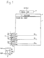
- Figure 1 is a circuit diagram schematically illustrating a first embodiment of the invention.
- Figure 2 is a circuit diagram schematically illustrating a second embodiment of the invention.
- Figure 3 is a circuit diagram schematically illustrating a third embodiment of the invention.
- Figure 1 shows an embodiment of the invention.
- This embodiment is a ROM comprising a memory cell array 1 , a Y-decoder 2 , a sense amplifier 3 , a word line driving unit 4 , and a word line test switch circuit 5 .
- the memory cell array 1 has a large number of memory cells (not shown) which are arranged in a matrix form. Each memory cell is selected when the word line to which the memory cell is connected is driven by the word line driving unit 4 . The data stored in the selected memory cell is output on the bit line (not shown in Figure 1) connected to the memory cell and is transferred through the Y-decoder 2 to the sense amplifier 3 .
- the word line driving unit 4 consists of driving circuits C 0 , C 1 , C 2 , ⁇ which drive the word lines WL 0 , WL 1 , WL 2 , ⁇ , respectively.
- Each of the driving circuits has a PMOS transistor Q 1 and an NMOS transistor Q 2 .
- the source and drain of the PMOS transistor Q 1 are respectively connected to the Vcc level and the drain of the NMOS transistor Q 2 .
- Each respective one of control signals IN 0 , IN 1 , IN 2 , ⁇ is applied to the gates of the transistors Q 1 and Q 2 .
- the source of the NMOS transistor Q 2 is connected to the ground.
- the source of the NMOS transistor Q 2 is connected to the output of the word line test switch circuit 5 .
- the control signals IN 0 , IN 1 , IN 2 , ⁇ are normally set to the Vcc level, keeping the NMOS transistors Q 2 in conduction and therefore holding the respective word lines either at the ground level or at the same level as the output signal of the word line test switch circuit 5 .
- the control signal applied to the driving circuit which drives the word line connected to that memory cell is set low, causing the PMOS transistor Q 1 in that driving circuit to conduct and thereby setting the word line to the Vcc level.
- the word line test switch circuit 5 comprises NMOS transistors Q 3 and Q 4 and an inverter 6 .
- the source of the transistor Q 4 is connected to the ground, and the source of the NMOS transistor Q 3 is connected to the drain of the NMOS transistor Q 4 .
- a test signal TEST is applied to the drain of the NMOS transistor Q 3 .
- An inverted test signal TEST ⁇ is applied directly to the gate of the NMOS transistor Q 4 , and to the gate of the NMOS transistor Q 3 via the inverter 6 .
- the test signal TEST and inverted test signal TEST ⁇ are set at the Vcc and ground levels respectively. Therefore, a high level signal which is given by subtracting the threshold value Vth of the NMOS transistor Q 3 from the Vcc level is output from the circuit 5 in the test mode, while, in non-test mode, a signal of the ground level is output.
- the test signal TEST is set to the Vcc level while holding all the control signals IN 0 , IN 1 , IN 2 , ⁇ applied to the word line driving circuits C 0 , C 1 , C 2 , ⁇ at the Vcc level. This causes the NMOS transistors Q 2 in the driving circuits C 0 , C 1 , C 2 , ⁇ and the NMOS transistor Q 3 in the test switch circuit 5 to be conductive.
- the even-numbered word lines WL 0 , WL 2 , ⁇ are set to the ground level, while on the other hand, the odd-numbered word lines WL 1 , WL 3 , ⁇ are driven high since the output signal of the test switch circuit 5 is set high. Because of the thus provided difference between the potential applied to the even-numbered word lines and that applied to the odd-numbered word lines, it is expected that a current Itw will flow through the output of the test switch circuit 5 if there is any short circuit between adjacent word lines. Therefore, by measuring this current, it is possible to check in a short period of time for failures resulting from word line shorting.
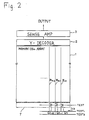
- Figure 2 shows a second embodiment of the invention.
- the embodiment of Figure 2 comprises a memory cell array 1 , a Y-decoder 2 , and a sense amplifier 3 , as in the foregoing embodiment of Figure 1.
- the word lines and the word line driving unit are not shown in Figure 2.
- the sources of the NMOS transistors Q i are connected to the ends of respective bit lines BL i .
- a test signal TEST is coupled to the gates of the NMOS transistors Q i , a signal TEST 1 is coupled to the drains of the transistors connected to the even-numbered bit lines, and a signal TEST 2 is coupled to the drains of the transistors connected to the odd-numbered bit lines.
- test signal TEST In the test mode, all the word lines are placed in a non-selected state, and the test signal TEST is set to the Vcc level, causing all the NMOS transistors Q i to be conductive. Under this condition, the signal TEST 1 is set to a high level and the signal TEST 2 to the ground level, thereby setting the even-numbered bit lines to a high level and the odd-numbered bit lines to the ground level. Therefore, by measuring the current Itb flowing through the signal line for the signal TEST 1 , it is possible to check for short circuits between adjacent bit lines in a short period of time.
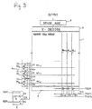
- FIG 3 shows a third embodiment of the invention.
- This embodiment is a ROM having the same configuration as that of the ROM of Figure 1 and provided with the bit line test switch circuit shown in Figure 2.
- the configuration of this embodiment permits the testing for shorts not only between adjacent word lines but also between adjacent bit lines. Furthermore, by combining these two test modes, it is also possible to check for defects in contacts of bit lines and memory cell transistors, the gate oxide film of a memory cell transistor, etc.
Landscapes
- For Increasing The Reliability Of Semiconductor Memories (AREA)
- Read Only Memory (AREA)
- Semiconductor Integrated Circuits (AREA)
- Semiconductor Memories (AREA)
- Dram (AREA)
- Testing Or Measuring Of Semiconductors Or The Like (AREA)
Applications Claiming Priority (2)
| Application Number | Priority Date | Filing Date | Title |
|---|---|---|---|
| JP2274803A JP2647546B2 (ja) | 1990-10-11 | 1990-10-11 | 半導体記憶装置のテスト方法 |
| JP274803/90 | 1990-10-11 |
Publications (3)
| Publication Number | Publication Date |
|---|---|
| EP0480752A2 EP0480752A2 (en) | 1992-04-15 |
| EP0480752A3 EP0480752A3 (en) | 1993-02-24 |
| EP0480752B1 true EP0480752B1 (en) | 1997-02-05 |
Family
ID=17546787
Family Applications (1)
| Application Number | Title | Priority Date | Filing Date |
|---|---|---|---|
| EP91309384A Expired - Lifetime EP0480752B1 (en) | 1990-10-11 | 1991-10-11 | Semiconductor memory device with short circuit identifying means |
Country Status (6)
| Country | Link |
|---|---|
| US (1) | US5331594A (enExample) |
| EP (1) | EP0480752B1 (enExample) |
| JP (1) | JP2647546B2 (enExample) |
| KR (1) | KR960001300B1 (enExample) |
| DE (1) | DE69124562T2 (enExample) |
| TW (1) | TW218935B (enExample) |
Families Citing this family (38)
| Publication number | Priority date | Publication date | Assignee | Title |
|---|---|---|---|---|
| JP2793427B2 (ja) * | 1992-04-08 | 1998-09-03 | 株式会社東芝 | 半導体装置 |
| JP2978329B2 (ja) * | 1992-04-21 | 1999-11-15 | 三菱電機株式会社 | 半導体メモリ装置及びそのビット線の短絡救済方法 |
| DE4223532A1 (de) * | 1992-07-17 | 1994-01-20 | Philips Patentverwaltung | Schaltungsanordnung zum Prüfen der Adressierung wenigstens einer Matrix |
| US5428621A (en) * | 1992-09-21 | 1995-06-27 | Sundisk Corporation | Latent defect handling in EEPROM devices |
| JP3164939B2 (ja) * | 1993-04-27 | 2001-05-14 | 富士通株式会社 | 記憶装置の試験回路を備えた装置 |
| DE69326329T2 (de) * | 1993-06-28 | 2000-04-13 | Stmicroelectronics S.R.L., Agrate Brianza | Speicherzellen-Stromleseverfahren in Mikrosteuergerät |
| JP3354231B2 (ja) * | 1993-09-29 | 2002-12-09 | 三菱電機エンジニアリング株式会社 | 半導体装置 |
| KR950015768A (ko) * | 1993-11-17 | 1995-06-17 | 김광호 | 불휘발성 반도체 메모리 장치의 배선단락 검출회로 및 그 방법 |
| KR0122100B1 (ko) * | 1994-03-10 | 1997-11-26 | 김광호 | 스트레스회로를 가지는 반도체집적회로 및 그 스트레스전압공급방법 |
| KR0135231B1 (ko) * | 1994-08-23 | 1998-04-22 | 김주용 | 고속 테스트 기능을 갖는 메모리 소자 |
| US5610866A (en) * | 1994-10-31 | 1997-03-11 | Sgs-Thomson Microelectronics, Inc. | Circuit structure and method for stress testing of bit lines |
| US5623925A (en) * | 1995-06-05 | 1997-04-29 | Cmed, Inc. | Virtual medical instrument for performing medical diagnostic testing on patients |
| JP3734853B2 (ja) * | 1995-06-27 | 2006-01-11 | 株式会社ルネサステクノロジ | 半導体記憶装置 |
| DE19612441C2 (de) * | 1996-03-28 | 1998-04-09 | Siemens Ag | Schaltungsanordnung mit einer Testschaltung |
| US6072719A (en) | 1996-04-19 | 2000-06-06 | Kabushiki Kaisha Toshiba | Semiconductor memory device |
| US5781557A (en) * | 1996-12-31 | 1998-07-14 | Intel Corporation | Memory test mode for wordline resistive defects |
| FR2771840B1 (fr) * | 1997-11-28 | 2003-06-27 | Sgs Thomson Microelectronics | Memoire rom testable en consommation statique |
| KR19990084215A (ko) * | 1998-04-03 | 1999-12-06 | 윤종용 | 반도체 메모리 장치의 라인-브리지 차단 회로 |
| DE69937559T2 (de) | 1999-09-10 | 2008-10-23 | Stmicroelectronics S.R.L., Agrate Brianza | Nicht-flüchtige Speicher mit Erkennung von Kurzschlüssen zwischen Wortleitungen |
| US6407953B1 (en) | 2001-02-02 | 2002-06-18 | Matrix Semiconductor, Inc. | Memory array organization and related test method particularly well suited for integrated circuits having write-once memory arrays |
| US6388927B1 (en) * | 2001-02-23 | 2002-05-14 | Cypress Semiconductor Corp. | Direct bit line-bit line defect detection test mode for SRAM |
| US6768685B1 (en) | 2001-11-16 | 2004-07-27 | Mtrix Semiconductor, Inc. | Integrated circuit memory array with fast test mode utilizing multiple word line selection and method therefor |
| US6778449B2 (en) * | 2002-07-01 | 2004-08-17 | International Business Machines Corporation | Method and design for measuring SRAM array leakage macro (ALM) |
| US7765153B2 (en) * | 2003-06-10 | 2010-07-27 | Kagi, Inc. | Method and apparatus for verifying financial account information |
| US6992939B2 (en) * | 2004-01-26 | 2006-01-31 | Micron Technology, Inc. | Method and apparatus for identifying short circuits in an integrated circuit device |
| US7053647B2 (en) * | 2004-05-07 | 2006-05-30 | Taiwan Semiconductor Manufacturing Co., Ltd. | Method of detecting potential bridging effects between conducting lines in an integrated circuit |
| KR100902052B1 (ko) * | 2007-08-13 | 2009-06-15 | 주식회사 하이닉스반도체 | 워드 라인 테스트 방법 |
| JP2009076176A (ja) * | 2007-09-25 | 2009-04-09 | Toshiba Corp | 不揮発性半導体記憶装置 |
| TWI534819B (zh) * | 2014-07-31 | 2016-05-21 | 常憶科技股份有限公司 | 於靜態電流測試下檢測全域字元線缺陷 |
| US9330783B1 (en) * | 2014-12-17 | 2016-05-03 | Apple Inc. | Identifying word-line-to-substrate and word-line-to-word-line short-circuit events in a memory block |
| US9390809B1 (en) | 2015-02-10 | 2016-07-12 | Apple Inc. | Data storage in a memory block following WL-WL short |
| US9529663B1 (en) | 2015-12-20 | 2016-12-27 | Apple Inc. | Detection and localization of failures in 3D NAND flash memory |
| US9996417B2 (en) | 2016-04-12 | 2018-06-12 | Apple Inc. | Data recovery in memory having multiple failure modes |
| US10755787B2 (en) | 2018-06-28 | 2020-08-25 | Apple Inc. | Efficient post programming verification in a nonvolatile memory |
| US10762967B2 (en) | 2018-06-28 | 2020-09-01 | Apple Inc. | Recovering from failure in programming a nonvolatile memory |
| US10936455B2 (en) | 2019-02-11 | 2021-03-02 | Apple Inc. | Recovery of data failing due to impairment whose severity depends on bit-significance value |
| US10915394B1 (en) | 2019-09-22 | 2021-02-09 | Apple Inc. | Schemes for protecting data in NVM device using small storage footprint |
| US11550657B1 (en) | 2021-09-01 | 2023-01-10 | Apple Inc. | Efficient programming schemes in a nonvolatile memory |
Family Cites Families (17)
| Publication number | Priority date | Publication date | Assignee | Title |
|---|---|---|---|---|
| JPS57105897A (en) * | 1980-12-23 | 1982-07-01 | Fujitsu Ltd | Semiconductor storage device |
| US4393475A (en) * | 1981-01-27 | 1983-07-12 | Texas Instruments Incorporated | Non-volatile semiconductor memory and the testing method for the same |
| JPS592299A (ja) * | 1982-06-29 | 1984-01-07 | Fujitsu Ltd | フイ−ルドプログラマブル素子 |
| JPS62114200A (ja) * | 1985-11-13 | 1987-05-25 | Mitsubishi Electric Corp | 半導体メモリ装置 |
| US4685086A (en) * | 1985-11-14 | 1987-08-04 | Thomson Components-Mostek Corp. | Memory cell leakage detection circuit |
| JPS62120700A (ja) * | 1985-11-20 | 1987-06-01 | Fujitsu Ltd | 半導体記憶装置 |
| JPS63177400A (ja) * | 1987-01-19 | 1988-07-21 | Hitachi Ltd | 半導体メモリ |
| JP2609211B2 (ja) * | 1987-03-16 | 1997-05-14 | シーメンス・アクチエンゲゼルシヤフト | メモリセルの検査回路装置および方法 |
| JPS63244400A (ja) * | 1987-03-16 | 1988-10-11 | シーメンス・アクチエンゲゼルシヤフト | メモリセルの検査回路装置および方法 |
| JPH01109921A (ja) * | 1987-10-23 | 1989-04-26 | Ricoh Co Ltd | プログラマブルロジックアレイ |
| JPH01134799A (ja) * | 1987-11-20 | 1989-05-26 | Sony Corp | メモリ装置 |
| JPH01243291A (ja) * | 1988-03-25 | 1989-09-27 | Hitachi Ltd | メモリ回路 |
| JPH01276500A (ja) * | 1988-04-27 | 1989-11-07 | Hitachi Ltd | 半導体記憶装置 |
| JPH01296500A (ja) * | 1988-05-23 | 1989-11-29 | Mitsubishi Electric Corp | 半導体記憶装置 |
| JPH02249196A (ja) * | 1989-03-22 | 1990-10-04 | Hitachi Ltd | 半導体記憶装置 |
| JPH03137900A (ja) * | 1989-07-27 | 1991-06-12 | Nec Corp | 不揮発性半導体メモリ |
| JP2601931B2 (ja) * | 1990-04-06 | 1997-04-23 | 株式会社東芝 | 半導体不揮発性メモリ装置 |
-
1990
- 1990-10-11 JP JP2274803A patent/JP2647546B2/ja not_active Expired - Fee Related
-
1991
- 1991-10-09 TW TW080107965A patent/TW218935B/zh active
- 1991-10-10 US US07/776,052 patent/US5331594A/en not_active Expired - Lifetime
- 1991-10-10 KR KR1019910017788A patent/KR960001300B1/ko not_active Expired - Lifetime
- 1991-10-11 DE DE69124562T patent/DE69124562T2/de not_active Expired - Lifetime
- 1991-10-11 EP EP91309384A patent/EP0480752B1/en not_active Expired - Lifetime
Also Published As
| Publication number | Publication date |
|---|---|
| JPH04149900A (ja) | 1992-05-22 |
| JP2647546B2 (ja) | 1997-08-27 |
| EP0480752A2 (en) | 1992-04-15 |
| US5331594A (en) | 1994-07-19 |
| KR960001300B1 (ko) | 1996-01-25 |
| DE69124562D1 (de) | 1997-03-20 |
| DE69124562T2 (de) | 1997-08-14 |
| TW218935B (enExample) | 1994-01-11 |
| EP0480752A3 (en) | 1993-02-24 |
| KR920008768A (ko) | 1992-05-28 |
Similar Documents
| Publication | Publication Date | Title |
|---|---|---|
| EP0480752B1 (en) | Semiconductor memory device with short circuit identifying means | |
| US4779272A (en) | Testable variable-threshold non-volatile semiconductor memory | |
| US5276647A (en) | Static random access memory including stress test circuitry | |
| EP0293339B1 (en) | Nonvolatile memory device with a high number of cycle programming endurance | |
| JP3076606B2 (ja) | 半導体記憶装置およびその検査方法 | |
| US4720818A (en) | Semiconductor memory device adapted to carry out operation test | |
| US5424988A (en) | Stress test for memory arrays in integrated circuits | |
| US3995215A (en) | Test technique for semiconductor memory array | |
| US5124945A (en) | Method and apparatus for verifying the state of a plurality of electrically programmable memory cells | |
| US5265057A (en) | Semiconductor memory | |
| KR100339321B1 (ko) | 복수의메모리셀을가진메모리를구비한전자회로 | |
| JP4088143B2 (ja) | 不揮発性半導体記憶装置及び行線短絡不良検出方法 | |
| US5684741A (en) | Auto-verification of programming flash memory cells | |
| CN1103985A (zh) | 测试静态ram的方法和装置 | |
| EP0509360B1 (en) | Dynamic random access memory device with multiple word line selector used in burn-in test | |
| US4744058A (en) | Semiconductor programmable memory device and method of writing a predetermined pattern to same | |
| US4800332A (en) | Reconfigurable integrated circuit with enhanced testability of memory cell leakage | |
| KR100367191B1 (ko) | 테스트수단을구비한전자회로및메모리셀테스트방법 | |
| EP0492610B1 (en) | Dynamic random access memory | |
| JP3267301B2 (ja) | 検査回路を有する回路装置 | |
| KR0185643B1 (ko) | 반도체 메모리장치의 스트레스 전압 인가장치 | |
| EP0760518B1 (en) | Circuitry and methodology to test single bit failures of integrated circuit memory devices | |
| US5615166A (en) | Semiconductor memory integrated circuit | |
| US5812460A (en) | Nonvolatile semiconductor memory device having test circuit for testing erasing function thereof | |
| KR950004871B1 (ko) | 중복회로가 있는 반도체기억장치 및 그중복회로의 사용여부를 확보하는 검사방법 |
Legal Events
| Date | Code | Title | Description |
|---|---|---|---|
| PUAI | Public reference made under article 153(3) epc to a published international application that has entered the european phase |
Free format text: ORIGINAL CODE: 0009012 |
|
| AK | Designated contracting states |
Kind code of ref document: A2 Designated state(s): DE FR GB IT NL |
|
| PUAL | Search report despatched |
Free format text: ORIGINAL CODE: 0009013 |
|
| AK | Designated contracting states |
Kind code of ref document: A3 Designated state(s): DE FR GB IT NL |
|
| 17P | Request for examination filed |
Effective date: 19930525 |
|
| 17Q | First examination report despatched |
Effective date: 19951208 |
|
| GRAG | Despatch of communication of intention to grant |
Free format text: ORIGINAL CODE: EPIDOS AGRA |
|
| GRAH | Despatch of communication of intention to grant a patent |
Free format text: ORIGINAL CODE: EPIDOS IGRA |
|
| GRAH | Despatch of communication of intention to grant a patent |
Free format text: ORIGINAL CODE: EPIDOS IGRA |
|
| GRAA | (expected) grant |
Free format text: ORIGINAL CODE: 0009210 |
|
| AK | Designated contracting states |
Kind code of ref document: B1 Designated state(s): DE FR GB IT NL |
|
| ITF | It: translation for a ep patent filed | ||
| REF | Corresponds to: |
Ref document number: 69124562 Country of ref document: DE Date of ref document: 19970320 |
|
| ET | Fr: translation filed | ||
| PLBE | No opposition filed within time limit |
Free format text: ORIGINAL CODE: 0009261 |
|
| STAA | Information on the status of an ep patent application or granted ep patent |
Free format text: STATUS: NO OPPOSITION FILED WITHIN TIME LIMIT |
|
| 26N | No opposition filed | ||
| REG | Reference to a national code |
Ref country code: GB Ref legal event code: IF02 |
|
| PGFP | Annual fee paid to national office [announced via postgrant information from national office to epo] |
Ref country code: FR Payment date: 20101020 Year of fee payment: 20 Ref country code: NL Payment date: 20101016 Year of fee payment: 20 |
|
| PGFP | Annual fee paid to national office [announced via postgrant information from national office to epo] |
Ref country code: DE Payment date: 20101006 Year of fee payment: 20 |
|
| PGFP | Annual fee paid to national office [announced via postgrant information from national office to epo] |
Ref country code: IT Payment date: 20101020 Year of fee payment: 20 Ref country code: GB Payment date: 20101006 Year of fee payment: 20 |
|
| REG | Reference to a national code |
Ref country code: DE Ref legal event code: R071 Ref document number: 69124562 Country of ref document: DE |
|
| REG | Reference to a national code |
Ref country code: DE Ref legal event code: R071 Ref document number: 69124562 Country of ref document: DE |
|
| REG | Reference to a national code |
Ref country code: NL Ref legal event code: V4 Effective date: 20111011 |
|
| REG | Reference to a national code |
Ref country code: GB Ref legal event code: PE20 Expiry date: 20111010 |
|
| PG25 | Lapsed in a contracting state [announced via postgrant information from national office to epo] |
Ref country code: NL Free format text: LAPSE BECAUSE OF EXPIRATION OF PROTECTION Effective date: 20111011 |
|
| PG25 | Lapsed in a contracting state [announced via postgrant information from national office to epo] |
Ref country code: GB Free format text: LAPSE BECAUSE OF EXPIRATION OF PROTECTION Effective date: 20111010 |
|
| PG25 | Lapsed in a contracting state [announced via postgrant information from national office to epo] |
Ref country code: DE Free format text: LAPSE BECAUSE OF EXPIRATION OF PROTECTION Effective date: 20111012 |