EP0444201A1 - Procede de production d'un filtre de couleur - Google Patents
Procede de production d'un filtre de couleur Download PDFInfo
- Publication number
- EP0444201A1 EP0444201A1 EP90913534A EP90913534A EP0444201A1 EP 0444201 A1 EP0444201 A1 EP 0444201A1 EP 90913534 A EP90913534 A EP 90913534A EP 90913534 A EP90913534 A EP 90913534A EP 0444201 A1 EP0444201 A1 EP 0444201A1
- Authority
- EP
- European Patent Office
- Prior art keywords
- resist
- light
- black matrix
- insulating
- color filter
- Prior art date
- Legal status (The legal status is an assumption and is not a legal conclusion. Google has not performed a legal analysis and makes no representation as to the accuracy of the status listed.)
- Withdrawn
Links
Images


Classifications
-
- G—PHYSICS
- G03—PHOTOGRAPHY; CINEMATOGRAPHY; ANALOGOUS TECHNIQUES USING WAVES OTHER THAN OPTICAL WAVES; ELECTROGRAPHY; HOLOGRAPHY
- G03F—PHOTOMECHANICAL PRODUCTION OF TEXTURED OR PATTERNED SURFACES, e.g. FOR PRINTING, FOR PROCESSING OF SEMICONDUCTOR DEVICES; MATERIALS THEREFOR; ORIGINALS THEREFOR; APPARATUS SPECIALLY ADAPTED THEREFOR
- G03F7/00—Photomechanical, e.g. photolithographic, production of textured or patterned surfaces, e.g. printing surfaces; Materials therefor, e.g. comprising photoresists; Apparatus specially adapted therefor
- G03F7/0005—Production of optical devices or components in so far as characterised by the lithographic processes or materials used therefor
- G03F7/0007—Filters, e.g. additive colour filters; Components for display devices
-
- G—PHYSICS
- G02—OPTICS
- G02B—OPTICAL ELEMENTS, SYSTEMS OR APPARATUS
- G02B5/00—Optical elements other than lenses
- G02B5/20—Filters
-
- G—PHYSICS
- G02—OPTICS
- G02F—OPTICAL DEVICES OR ARRANGEMENTS FOR THE CONTROL OF LIGHT BY MODIFICATION OF THE OPTICAL PROPERTIES OF THE MEDIA OF THE ELEMENTS INVOLVED THEREIN; NON-LINEAR OPTICS; FREQUENCY-CHANGING OF LIGHT; OPTICAL LOGIC ELEMENTS; OPTICAL ANALOGUE/DIGITAL CONVERTERS
- G02F1/00—Devices or arrangements for the control of the intensity, colour, phase, polarisation or direction of light arriving from an independent light source, e.g. switching, gating or modulating; Non-linear optics
- G02F1/01—Devices or arrangements for the control of the intensity, colour, phase, polarisation or direction of light arriving from an independent light source, e.g. switching, gating or modulating; Non-linear optics for the control of the intensity, phase, polarisation or colour
- G02F1/13—Devices or arrangements for the control of the intensity, colour, phase, polarisation or direction of light arriving from an independent light source, e.g. switching, gating or modulating; Non-linear optics for the control of the intensity, phase, polarisation or colour based on liquid crystals, e.g. single liquid crystal display cells
- G02F1/133—Constructional arrangements; Operation of liquid crystal cells; Circuit arrangements
- G02F1/1333—Constructional arrangements; Manufacturing methods
- G02F1/1335—Structural association of cells with optical devices, e.g. polarisers or reflectors
- G02F1/133509—Filters, e.g. light shielding masks
- G02F1/133512—Light shielding layers, e.g. black matrix
-
- G—PHYSICS
- G02—OPTICS
- G02F—OPTICAL DEVICES OR ARRANGEMENTS FOR THE CONTROL OF LIGHT BY MODIFICATION OF THE OPTICAL PROPERTIES OF THE MEDIA OF THE ELEMENTS INVOLVED THEREIN; NON-LINEAR OPTICS; FREQUENCY-CHANGING OF LIGHT; OPTICAL LOGIC ELEMENTS; OPTICAL ANALOGUE/DIGITAL CONVERTERS
- G02F1/00—Devices or arrangements for the control of the intensity, colour, phase, polarisation or direction of light arriving from an independent light source, e.g. switching, gating or modulating; Non-linear optics
- G02F1/01—Devices or arrangements for the control of the intensity, colour, phase, polarisation or direction of light arriving from an independent light source, e.g. switching, gating or modulating; Non-linear optics for the control of the intensity, phase, polarisation or colour
- G02F1/13—Devices or arrangements for the control of the intensity, colour, phase, polarisation or direction of light arriving from an independent light source, e.g. switching, gating or modulating; Non-linear optics for the control of the intensity, phase, polarisation or colour based on liquid crystals, e.g. single liquid crystal display cells
- G02F1/133—Constructional arrangements; Operation of liquid crystal cells; Circuit arrangements
- G02F1/1333—Constructional arrangements; Manufacturing methods
- G02F1/1345—Conductors connecting electrodes to cell terminals
Definitions
- the present invention relates to a method of producing a color filter having a coloring matter layer prepared by a micellar disruption method, and relates to a resist for a light-shielding film used in this method for forming a black matrix.
- the above dyeing method (1) has a disadvantage in that the resultant filter has poor light resistance.
- the above dispersion method (2) shows a poor productivity due to a complexity of the steps.
- the above printing method (3) is unsuperior in accuracy and light resistance.
- the above electrodeposition method (4) is advantageous since the resultant filter has good light resistance and high heat resistance.
- the resultant filter needs a transparent electrode for forming a coloring matter layer, and also needs, on its surface, an electrode for driving a crystal liquid as is the same case with the above methods (1) to (3).
- Japanese Patent Application Laid-Open Gazette No. 63-243298 discloses a micellar disruption method which comprises forming a transparent electrode in a desired shape on an insulating substrate, and forming a porous hydrophobic coloring matter film on the electrode by a micellar disruption method.
- a light-shielding film is indispensable to make a display device such as a color filter, a liquid crystal display material, an electron display material, and a color display.
- display devices have widely been used in several fields such as a lap-top personal computer, a note type personal computer, an audio equipment, an inside panel for an automotive, a clock, a calculator, a video cassette deck, a facsimile, a communication equipment, a game machine and a measurement equipment.
- a light-shielding film is used as a black matrix to be formed between each of picture elements such as red (R), green (G) and blue (B).
- Such black matrix is used to avoid lowering contrast and color purity due to leaked light.
- each picture element coloring matter layer
- a dispersion method or a dyeing method there have been used a carbon type photo-resist material and a chromium film in many cases.
- the use of the carbon type photo-resist material or the chromium film cannot give an electrode for driving a liquid crystal and an electrode for forming a coloring matter film at the same time due to their conductivity. More specifically, when a black matrix is first formed, using the photo-resist material or the chromium film, on an ITO electrode on which a pattern was formed for forming a coloring matter layer, the ITO electrode will be electrically connected with a right and left side electrodes. Thus, a coloring matter layer cannot be formed by a micellar disruption method and the like.
- the light-shielding film made from the conventional insulating organic dye type photo-resist material is formed by a photo-lithography method by mixing three kinds of photo-resists including dyes for red (R), green (G) and blue (B), or two kinds of photo-resists including dyes of red (R) and blue (B).
- the resultant light-shielding film has poor light-shielding ratio. To obtain a sufficient light-shielding ratio, it is necessary to make film thicker.
- the present invention was made in view of the above situations, and has its object to provide a process for producing a color filter in which a transparent electrode can be used both for forming a coloring matter layer during the color filter preparation and for driving a liquid crystal after the development. Further, it is another object of the present invention to provide a resist for a light-shielding film capable of forming a light-shielding film having an good insulating property and a high light-shielding ratio.
- an insulating black matrix and an electrode contact window belt for taking out an electrode in a part of a color filter are formed at the same time, and then a conductive coloring matter layer is laminated on a transparent electrode by a micellar disruption method.
- a micellar disruption method it is easy to produce a color filter in which an electrode for forming a coloring matter layer can be used also for driving a liquid crystal.
- the resists for light-shielding film of this invention include a resist for a light-shielding film comprising at least one of an insulating organic dye dispersed resist and an insulating transparent resist, and a conductive high light-shielding resist (first resist); a resist for light-shielding film comprising two or more kinds of insulating organic dye dispersed resists (second resist); and a resist for a light-shielding film composed of an insulating transparent resist containing a black organic dye dispersed therein (third resist).
- the resultant light-shielding film preferably has a surface resistance of not less than 107 ⁇ /cm2.
- Fig. 1 is a schematic cross-sectional view of one example of the color filter according to the present invention
- Fig. 2 is a plan view showing a mask for forming a transparent electrode
- Fig. 3 is a plan view showing a mask for forming a black matrix and an electrode contact zone
- Figs. 4 and 5 are cross-sectional views of an electrode contact zone
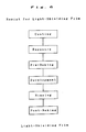
- Fig. 6 is a flow chart showing one example of production steps of a light-shielding film by way of a photo-lithography method.
- 1 denotes a glass substrate
- 2 denotes a transparent electrode
- 3 denotes a black stripe
- 4 denotes a coloring matter
- 5 denotes a coating layer
- 6 denotes an orientation layer.
- a black matrix is first formed over electrodes other than those corresponding to the individual separated colors.
- the material for the black matrix forms insulating layers as electrode contact window belts.
- electrically conductive layers are formed on the matrix so that the electrodes connect within each electrode contact window belt unit, but do not connect with those in different electrode contact window belt units.
- the coloring matter layer is formed by the micellar disruption method.
- a surface of an insulating glass substrate 1 (for example, plates of blue plate glass, non-alkali glass and quartz glass) is sufficiently washed with an alkali aqueous solution or pure water.
- a transparent electrode material layer is formed on one side of the glass substrate 1 by way of a vapor deposition method, a sputtering method, a bio-sol method, a ultra small particle casting method or the like.
- the electrode material layer is subjected to surface oxidation treatment or baking treatment to adjust resistance.
- a resist material (such as UV curable resin) is coated on the electrode material layer by a spin coating method, a dipping method or a casting method.
- the coated substrate is subjected to exposure treatment (for example, UV exposure) using a suitable mask, and the uncured portions of the resist material are washed and removed after development.
- the remaining resist material is cured, and the exposed electrode material is subjected to etching treatment with an etching liquid to remove the resist layer.
- the treated substrate is washed and transparent electrodes 2 (2B, 2G, 2R) corresponding to each of the primary colors are formed.
- a black matrix or stripe 3 is formed on the glass substrate 1 carrying the transparent electrodes 2 by a photo-lithography method as described in detail below.
- the resist for a light-shielding film of the present invention such as a resist material consisting of a UV curable resin and a black dye is coated on the substrate with a spin coater or a roll coater.
- the resist is subjected to exposure treatment with a suitable mask for a black stripe, followed by usual procedures including washing, development, washing and baking.
- electrode contact window belts can be formed in a part of a color filter simultaneously with formation of a black matrix.
- a repeating unit consisting of three electrode lines (shortest line 2B, medium size line 2G, longest line 2R) so that electrode lines 2B, 2G and 2R respectively correspond to these lines 21B, 21G and 21R for the three primary colors of a light, blue (B), green (G) and red (R).
- a black matrix is formed using, for example, a mask 30 as shown in Fig. 3.
- the mask 30 has a pattern 32 for forming electrode contact zones as well as a pattern 31 for forming a black matrix.
- a pattern 32 is composed of patterns for forming three electrode contact window belts, which consist of a pattern 32B for forming an electrode contact window belt for an electrode line (B); a pattern 32G for forming an electrode contact window belt for an electrode line (G); and a pattern 32R for forming an electrode contact window belt for an electrode line (R). It is preferable to use the resist for a light-shielding film according to the present invention to form a black matrix and an insulating layer at the same time.
- Electrode contact zones of a color filter prepared by using the mask 20 and the mask 30 are shown in Figs. 4 and 5.
- Fig. 4 is a cross-sectional view, taken along line IV-IV in the mask 30, of a color filter; and
- Fig. 5 is a cross-sectional view, taken along line V-V in the mask 30, of a color filter.
- the electrode lines 2G and 2R are coated with an insulating layer 41, but the electrode lines 2B are electrically connected with each other through a conductive layer 42.
- the resist for a light-shielding film according to the present invention suitably used for forming the above black matrix, will be described in detail below.
- the first resist of the present invention comprises at least one of an insulating organic dye dispersed resist and an insulating transparent resist, and a conductive high light-shielding resist.
- the insulating organic dye dispersed resists include, for example, a resist in which an insulating organic dye is dispersed, such as an acryl type resist, an epoxy type resist and a polyimide type resist.
- the insulating organic dyes include, for example, perylene type dyes, anthraquinone type dyes, dianthraquinone dyes, azo type dyes, diazo type dyes, quinacridone type dyes, and anthracene type dyes. More specifically, examples of the insulating organic dyes are a perylene dye, quinacridone, Naphthol AS, a shikonin dye, dianthraquinone, Sudan I, II, III or R, bisazo, and benzopyran.
- the blue dyes include, for example, phthalocyanine type dyes, copper phthalocyanine type dyes, indathrone type dyes, indophenol type dyes and cyanine type dyes. More specifically, examples of the blue dyes are metal complexes of phthalocyanine such as chlorinated copper phthalocyanine, chlorinated aluminum phthalocyanine, vanadic acid phthalocyanine, magnesium phthalocyanine, zinc phthalocyanine, iron phthalocyanine, cobalt phthalocyanine; phthalocyanine; merocyanine; and indophenol blue.
- phthalocyanine type dyes such as chlorinated copper phthalocyanine, chlorinated aluminum phthalocyanine, vanadic acid phthalocyanine, magnesium phthalocyanine, zinc phthalocyanine, iron phthalocyanine, cobalt phthalocyanine; phthalocyanine; merocyanine; and indophenol blue.
- organic dye dispersed resist containing a yellow (Y) organic dye, a violet (V) organic dye and the like are available in addition to resists containing a red (R), green (G) or blue (B) organic dye.
- the insulating transparent resists include any transparent resists having an insulating property, for example, UV curable resists. More specifically, the insulating resists include ALONIX (acryl type resin; Manufactured by Toa Gosei, Co.); and TORAY PHOTONIS (Manufactured by Toray, Co.)
- the conductive resists having a high light-shielding property include, for example, a conductive particle dispersed resists which are those resists containing conductive particles dispersed in a acryl type resist, an epoxy type resist and a polyimide type resist.
- examples of the conductive particles are high light-shielding materials such as carbon, chromium oxide and small metal particles.
- the first resist containing the above resists are usually prepared by mixing the above resists. Further, for instance, the first resist can be prepared by dispersing insulating organic dye and conductive high light shielding particles in one of the resist materials. In any preparation methods, it is preferable to mix each dye and conductive particles with a resist so that they are uniformly dispersed in the resist material.
- the mixing ratio can be selected appropriately. However, in the case of using a micellar disruption method, it is preferable to select the mixing ratio so that resultant light-shielding film has a surface resistance of 107 ⁇ /cm2 or more.
- a solvent can be added.
- a mixing equipment which can avoid heat generation, is preferably used to prevent resists from being aggregated.
- the second resist comprises at least two kinds of insulating organic dye dispersed resist.
- the above description for the first resist can be applied to the insulating organic dye dispersed resists for the second resists.
- the preparation methods include, for example, a method comprising mixing two kinds of photo-resist materials, each having one color dye different from each other; and a method comprising mixing two dyes (two colors) with one of resist materials and then dispersing the dyes in the resist material.
- a method comprising mixing two kinds of photo-resist materials, each having one color dye different from each other; and a method comprising mixing two dyes (two colors) with one of resist materials and then dispersing the dyes in the resist material.
- the third resist is an insulating transparent resist containing a black organic dye dispersed therein.
- the above description about the insulating transparent resins can also be applied to the third resist.
- the black organic dyes include, for example, Perillene Black, Aniline Black, and Cyanine Black. Two or more kinds of the black organic dyes can be dispersed in the insulating transparent resist. It is preferable that the black organic dye be uniformly dispersed in the resist.
- first, second and third resists can be positive type or negative type UV curable resists, and can be EB resists, X-ray resists and the like.
- the above first, second or third resist it is preferable to use the above first, second or third resist to form a black matrix with the use of a photo-lithography method.
- Fig. 6 is a flow chart showing steps of production of a light-shielding film by way of a photo-lithography method.
- a coloring matter layer consisting of conductive porous and hydrophobic coloring matter thin film, is formed on a transparent electrode by way of a micelle-electrolytic method.
- conductive porous film means that the film or layer is porous so as to have enough conductance. In other words, the film or layer has conductance to extent that a transparent electrode located under the film or layer can be used for driving a liquid crystal and the like. Thus, the film or layer itself needs not to be conductive.
- micellar disruption method To form the above coloring matter thin film by a micellar disruption method, the following procedures can be used.
- a micelle forming agent comprising ferrocene derivatives and a coloring matter material (hydrophobic coloring matter) are added to an aqueous solvent having a controlled conductance prepared by adding, as necessary, a support electrolyte to water. The mixture is well stirred to obtain a micelle containing the coloring matter material therein.
- the micelle solution is subjected to electrolytic treatment, the micelle moves to an anode.
- the ferrocene derivative contained in the micelle loses an electron, e ⁇ (Fe2+ of the ferrocene is oxidized to Fe3+) on the anode (transparent electrode), and at the same time the micelle is broken.
- e ⁇ Fe2+ of the ferrocene is oxidized to Fe3+
- the oxidized ferrocene derivative moves to a cathode and receives an electron, e ⁇ to reform a micelle. While the micelle formation and breakage are repeated, coloring matter particles are precipitated on the transparent electrode to form a thin film.
- the desired coloring matter thin film is formed in this manner.
- the thus obtained coloring matter thin film has, in general, a thickness of 0.1 to 10.0 ⁇ m, preferably 0.1 to 2.0 ⁇ m. Due to the porous structure of the thin film, the thin film has high conductance. If the film thickness is less than 0.1 ⁇ m, the hue of the coloring matter layer cannot sufficiently be exhibited. If the thickness is more than 10.0 ⁇ m, the film will have low conductance. Thus, the thin film having the above thickness range is preferable.
- the micelle forming agents which can be used in a micellar disruption method are those comprising ferrocene derivatives.
- the ferrocene derivatives include several types, and may be those represented by the general formula [I]: wherein R1 and R2 are independently a C1 ⁇ 6 alkyl group, C1 ⁇ 6 alkoxy group, amino group, dimethylamino group, hydroxyl group, acetylamino group, carboxyl group, methoxycarbonyl group, acetoxy group, aldehyde group or halogen; R3 is hydrogen or a linear or branched C4 ⁇ 18 alkyl group or alkenyl group; R4 and R5 are independently hydrogen or a methyl group; Y is oxygen, an oxycarbonyl group or acyloxy group; a is an integer of 0 to 4; b is an integer of 0 to 4; m is an integer of 1 to 18; and n is a real number of 2.0 to 70.0.
- the C1 ⁇ 6 alkyl groups include a methyl group (CH3) and ethyl group (C2H5); the alkoxy groups include a methoxy group (OCH3) and ethoxy group (OC2H5); halogen includes chlorine, bromine, fluorine and iodine.
- R1 and R2 may be the same as or different from each other. Further, when R1 and R2 independently exist in a plurality of five-membered rings of the ferrocene, a plurality of substituted groups may be the same as or different from each other.
- the general formula [I] include, for example,
- n means a number of a repeating unit which is the above oxyalkylene group.
- the number "n” includes a real number of the repeated oxyalkylene group (thus means average number) as well as an integer of 2.0 to 70.0.
- the ferrocene derivatives which can be used in the micellar disruption method include several ones in addition to those represented by the general formula [I]. Such ferrocene derivatives include ammonium type, pyridine type (PCT International Publication WO 88/07538, etc.) and those described in patent specifications of JP Patent Appln. Nos.
- ferrocene derivatives are capable of effectively dissolving or dispersing hydrophobic substances in an aqueous medium.
- micellar disruption method used in the present invention, a micelle forming agent comprising a ferrocene derivative, a supporting salt, and a hydrophobic organic substance are placed in an aqueous medium and thoroughly dispersed by the use of supersonic waves, a homogenizer, or a stirrer to from a micelle. Thereafter, if necessary, an excessive coloring matter material is removed.
- the micelle solution thus obtained is subjected to electrolytic treatment using the transparent electrode while allowing to stand or somewhat stirring.
- the coloring matter material may be supplementarily added to the micelle solution, or there may be provided a recycle circuit in which the micelle solution in the vicinity of the anode is withdrawn out of the system.
- the concentration of micelle forming agent may be at least the critical micelle concentration, more specifically about 0.1 mM or more.
- concentration of the coloring matter material may be saturated concentration or higher.
- Electrolytic conditions are determined appropriately depending on various circumstances.
- the liquid temperature is 0 to 70 o C, preferably 5 to 40 o C.
- the voltage is not less than oxidation-reduction potential of the ferrocene derivative as micelle forming agent, but not greater than hydrogen generation potential, and more specifically is 0.03 to 1.00 V, preferably 0.15 to 0.7 V.
- the current density is not more than 10 mA/cm2, preferably 50 to 300 A/cm2.
- the reaction proceeds in accordance with the principle of the micellar disruption method.
- Fe2+ is converted into Fe3+ on an anode, leading to the breakdown of the micelle. Particles of a coloring matter material are deposited on the anode.
- Fe3+ oxidized on the anode is reduced to Fe2+, recovering the original micelle and, therefore, a film forming operation can be carried out repeatedly using the same solution.
- Electrolytic treatment as described above forms a thin film composed of the desired coloring matter material on the anode.
- the supporting salt (supporting electrolyte) to be used in the process of the present invention is added, if necessary, in order to control the electrical conductance of the aqueous medium.
- the amount of the supporting salt added is such that the precipitation of coloring matter material dissolved or dispersed is not prevented, and is usually about 0 to 300 times, preferably about 50 to 200 times that of the above micelle forming agents. It is possible to perform the electrolytic treatment without using the supporting salt. In this case, highly pure thin film containing no supporting salt is obtained.
- the type of the supporting salt is not critical as long as capable to control the electric conductance of the aqueous medium without inhibiting the formation of the micelle and the deposition of the above coloring matter material.
- the supporting salts which have widely been used include, for example, sulfuric acid salts (salts of lithium, potassium, sodium, rubidium, aluminum and the like); acetic acid salts (salts of lithium, potassium, sodium, rubidium, beryllium, magnesium, calcium, strontium, barium, aluminum and the like); salts of halogenated compounds (salts of lithium, potassium, sodium, rubidium, magnesium, calcium, aluminum and the like); and water-soluble oxide salts (salts of lithium, potassium, sodium, rubidium, magnesium, calcium, aluminum and the like).
- sulfuric acid salts saltsalts of lithium, potassium, sodium, rubidium, aluminum and the like
- acetic acid salts salts of lithium, potassium, sodium, rubidium, beryllium, magnesium, calcium, strontium, barium, aluminum and the like
- salts of halogenated compounds saltsalts of lithium, potassium, sodium, rubidium, magnesium, calcium, aluminum and the like
- water-soluble oxide salts salts
- the electrode to be used in the process of the present invention is sufficient to be a metal more noble than the oxidation potential (against +0.15V to 0.30V saturated calomel electrode) of ferrocene, or an electrically conductive substance. More specifically, ITO (mixed oxide of indium oxide and tin oxide), tin oxide, electrically conductive organic polymers, and the like can be used.
- the coloring matter materials for forming a coloring matter film include several ones including those exhibiting the three primary colors for light, such as a hydrophobic coloring matter material for red, green or blue.
- the red coloring matter materials include, for example, perylene type dyes, lake dyes, azo type dyes, quinacridone type dyes, anthraquinone type dyes and anthracene type dyes, and more specifically include a perylene dye, lake dyes (Ca, Ba, Sr, Mn), quinacridone, Naphthol AS, a shikonin dye, dianthraquinone, Sudan I, II, III or R, bisazo, and benzopyran, cadmium sulfide type dyes, Fe (III) oxide type dyes.
- the perylene dye and the lake dye are preferred.
- the green coloring matter materials include, for example, halogenated multi-substitued phthalocyanine type dyes, halogenated multi-substituted copper phthalocyanine type dyes and triphenylmethane type basic dyes, and more specifically include chlorinated multi-substituted phthalocyanine, its copper complex and a barium-triphenylmethane dye.
- the blue coloring matter materials include, for example, copper phthalocyanine type dyes, indathrone type dyes, indophenol type dyes and cyanine type dyes, and more specifically include metal complexes of phthalocyanine such as chlorinated copper phthalocyanine, chlorinated aluminum phthalocyanine, vanadic acid phthalocyanine, magnesium phthalocyanine, zinc phthalocyanine, iron phthalocyanine, cobalt phthalocyanine; phthalocyanine; merocyanine; and indophenol blue.
- phthalocyanine such as chlorinated copper phthalocyanine, chlorinated aluminum phthalocyanine, vanadic acid phthalocyanine, magnesium phthalocyanine, zinc phthalocyanine, iron phthalocyanine, cobalt phthalocyanine; phthalocyanine; merocyanine; and indophenol blue.
- any one of red, green and blue hydrophobic coloring matters is first added to an aqueous medium, and the first desired color thin film is formed by the above-mentioned micellar disruption method. Then, the micelle electrolytic treatment is repeatedly carried out using different hydrophobic coloring matter to form coloring matter films for the three primary colors (red, green, blue) on each transparent electrode.
- a top coating material may be coated with a spin coater or a roll coater on the coloring matter layer and a black matrix and dried at 80 to 150 o C for 5 to 60 minutes to form a conductive coating layer.
- the top coating material include, for example, an acryl resin, polyether resin, polyester resin, polyolefin resin, phosphazene resin, or polyphenylene sulfide resin.
- the coating layer allows a surface to be contacted with a liquid crystal to be flat. If the coating layer is prepared from a conductive material, voltage down due to the coating layer can be prevented. Further, transparent conductive particles such as ITO particles can be added to these coating materials.
- an orientation layer as the most upper layer may be formed by coating, for example, a polyamic acid monomer, a polyimide resin oligomer or the like by a spin coater or a roll coater, polymerizing the coated material at 200 to 300 o C for 30 minutes to 2 hours, washing with pure water or the like, and drying the polymerized product (at 60 to 100 o C for 30 minutes to 2 hours or by UV radiation or the like).
- the liquid crystals can be oriented by the orientation layer.
- a glass substrate (NA45; Manufactured by HOYA; size 320 x 300 x 0.5 mm) was washed with 0.1 N NaOH, and washed with pure water until the liquid resistance of the used water became 107 11cm2.
- the washed substrate was placed in a vacuum sputtering equipment and then subjected to sputtering treatment using ITO.
- the surface of the thus formed ITO layer was oxidized in air at 100 o C to adjust the surface resistance to 100 11cm2.
- a resist material (FH-2130; Manufactured by Fuji Hunt Electronics Technology, Co.) was coated over the ITO layer with a roller coater, baked at 80 o C for 5 minutes, subjected to UV radiation (60 seconds) with a 500W high pressure mercury lamp using a stripe mask as shown in Fig. 2.
- width of each line of the mask as shown in Fig. 2 was 90 ⁇ m, and distance between each line was 20 ⁇ m.
- the obtained product was washed with water, and the ITO coated with the resist material was immersed in a developing liquid (HPRD-410; Manufactured by Fuji Hunt Technology, Co.), and then developed for 5 minutes. Further, the obtained product was washed with pure water and then heated to 230 o C for 5 minutes. After sufficiently curing the resist material, the product was immersed in IN ⁇ HCl/IM ⁇ FeCl3 etching liquid to subject the ITO to etching treatment for 20 minutes. After etching, the product was washed with pure water, and the cured resist was removed with the use of a resist removing agent (Microstrip 2001; Manufactured by Fuji Hunt Technology, Co.). Then the product was further washed.
- a resist film was formed on the ITO carried substrate as prepared above, by coating a color resist containing a UV curable polymer and a black dye (Color Resist CK; Manufactured by Fuji Hunt Electronics Technology, Co.) by a spin coating at 3,000 rpm.
- the coated substrate was pre-baked at 80 o C for 5 minutes, and further coated with polyvinyl alcohol as oxygen resist material by spin coating at 400 rpm.
- the resist material was pre-baked at 80 o C for 5 minutes, and subjected to UV radiation with a 500W high pressure mercury lamp using a mask for black stripe as shown in Fig. 3.
- the substrate obtained as above was immersed in the red dye dispersed solution (an electrode contact zone was not immersed), and then micelle electrolytic treatment (0.5V, 25 o C, 30 minutes) was carried out using an electrode contact window belt for an electrode line for a red coloring matter.
- a saturated calomel electrode as reference electrode and an aluminum plate as cathode were used.
- the substrate was washed with pure water, baked at 180 o C for 1 hour to obtain a red coloring matter layer 4R.
- the average film thickness of each coloring matter layer was 0.5 ⁇ m (red), 0.4 ⁇ m (green) and 0.6 ⁇ m (blue), respectively.
- the obtained substrate was coated with a top coating material (OPTOMAR JHR; Manufacture by Nippon Synthetic Rubber) by spin coating at 3,000 rpm, and baked at 80 o C.
- the thus coated substrate was further coated with a N-methylpyrrolidone solution of polyamic acid by spin coating in the same manner, and the coated polyamic acid was polymerized under vacuum atmosphere at 250 o C for 1 hour. After washing with pure water, the washed substrate was dried at 80 o C for 1 hour to obtain a color filter of the present invention having a conductive coating layer 5 (0.2 ⁇ m) and an orientation layer 6 (0.1 ⁇ m).
- the color filter was subjected to sputtering treatment using ITO to form the ITO layer on the oriented layer 6.
- the resistance between this ITO and the ITO formed inside of the color filter was measured by a tester, and the resistance was 105 ⁇ /cm2.
- the insulating resistance between the ITOs was 1013 ⁇ /cm2.
- a glass substrate (NA45; Manufactured by HOYA; size 300 x 300 mm) having a surface resistance of 20 ⁇ /cm2 as an ITO film was coated with a 50 % xylene solution of a UV curable resist material (IC-28/T3; Manufactured by Fuji Hunt Electronics Technology) by spin coating at 1000 rpm. After spin coating, the coated substrate was pre-baked at 80 o C for 15 minutes. And then, this resist/ITO substrate was placed in an exposing equipment.
- IC-28/T3 UV curable resist material
- a mask used had a stripe pattern having a line width of 100 ⁇ m, a gap of 20 ⁇ m and a line length of 155 kN.
- a 2KW high pressure mercury lamp (exposure ability: 10mW/cm2 ⁇ s) was used. The proximity gap was set as 70 ⁇ m.
- the resist was developed with a developing liquid.
- the treated product was rinsed with pure water, and post-baked at 180 o C. And then, the product was subjected to etching treatment using an etching liquid consisting of 1M FeCl3, 1N HCl, 0.1N HNO3, 0.1 Ce(NO3)4. The etching treatment took 40 minutes. After etching, the product was washed with pure water, and the resist was removed by the use of 1N NaOH.
- the ITO electrode in the shape of strip was formed on the glass substrate.
- resist for a light-shielding film prepared by mixing a conductive high light-shielding resist (CK; Manufactured by Fuji Hunt Electronics Technology) and an insulating transparent resist (acryl type resist cellosolve acetate 10% solution; Manufactured by Toa Gosei) at a conductive resist/insulating resist ratio, by weight, of 3:1.
- CK conductive high light-shielding resist
- insulating transparent resist acryl type resist cellosolve acetate 10% solution
- the ITO patterning substrate as prepared above was rotated at 10 rpm, 30 cc of the above resist for a light-shielding film was sprayed thereon. Then, the substrate was subjected to spin coating at 2500 rpm to form an uniform film. The coated substrate was pre-baked at 80 o C for 15 minutes.
- the obtained product was subjected to exposure by an exposing machine having a 2kW high pressure mercury lamp and an alignment function, using a photo-mask for forming a black matrix pattern, while positioning the product. After that, the resist was developed using a color resist developing liquid (CD; diluted 4 times; Manufactured by Fuji Hunt Electronics Technology, Co.) for 30 seconds. The thus obtained product was rinsed with pure water, and then post-baked at 200 o C for 100 minutes. In this manner, the black stripe and the electrode contact window for each electrode line corresponding to each of the three primary colors, were formed at the same time.
- CD color resist developing liquid
- a micelle solution was prepared by adding a micelle forming age of a ferrocene derivative (Manufactured by Dohjin Chemical), LiBr (Manufactured by Wako Pure Chemical) and CROMOPHTHAL A2B (Manufactured by Chiba-Geigy) to 4L of pure water to prepare 2 mM/l solution, 0.1 M/l solution and 10g/l solution.
- the obtained solutions were stirred with a ultrasonic homogenizer for 30 minutes to obtain micelle solutions.
- the substrate prepared as above was immersed in the micelle solution (an electrode contact zone was not immersed).
- a red coloring matter layer for a color filter was formed by connecting an electrode line for a red coloring matter (stripe R) with a potentiostat, and carrying out constant potential electrolytic treatment at 0.5V. After the electrolytic treatment, the obtained product was washed with pure water, and pre-baked with an over at 180 o C.
- a green coloring matter layer and a blue coloring matter layer were formed in this order, using a green dye (Heliogen Green L9361; Manufactured by BASF), and a blue dye (Heliogen Blue B7080; Manufactured by BASF), respectively.
- a green dye Heliogen Green L9361; Manufactured by BASF
- a blue dye Heliogen Blue B7080; Manufactured by BASF
- the black stripe of the thus obtained color filter had a film thickness of 1.7 kN, a light-shielding ratio of 92% and a surface resistance of 109 ⁇ /cm2.
- the color filter was produced in such a way that the formed RGB filter had a thickness within 0.6 to 1.0 ⁇ m and had a relatively flat surface, and that the thin film was not formed on the electrodes other than those for passing electricity. In addition, it was found that the color filter had a resistance of 105 ⁇ /cm2, and that the color filter was an electrically conductive one.
- a resist for a light-shielding film prepared by mixing a conductive high light-shielding resist (CK; Manufactured by Fuji Hunt Electronics Technology), an insulating organic dye (red) dispersed resist (CR; Manufactured by Fuji Hunt Electronics Technology), an insulating organic dye (green) dispersed resist (CG; Manufactured by Fuji Hunt Electronics Technology), and an insulating organic dye (blue) dispersed resist (CB; Manufactured by Fuji Hunt Electronics Technology) at a CK/CR/CG/CB resist ratio, by weight, of 3:1:1:1, and that the rotation speed for spin coating was changed to 2000 rpm during black matrix formation, to produce a color filter.
- CK conductive high light-shielding resist
- CR insulating organic dye
- CG green
- blue blue
- the black matrix had a film thickness of 1.9 kN, and a light-shielding ratio of 93% which was extremely high.
- the black matrix had a surface resistance of 1010 ⁇ /cm2.
- Example 2 The same procedures as used in Example 2 were repeated except that there was used a resist for a light-shielding film prepared by mixing a conductive high light-shielding resist (CK; Manufactured by Fuji Hunt Electronics Technology), and an insulating transparent resist (acryl type resist ARONIX cellosolve acetate 10% solution; Manufactured by Toa Gosei) at a conductive resist/insulating resist ratio, by weight, of 1:1, and that the rotation speed for spin coating was changed to 1000 rpm during black matrix formation, to produce a color filter.
- CK conductive high light-shielding resist
- insulating transparent resist acryl type resist ARONIX cellosolve acetate 10% solution
- the black matrix had a film thickness of 2.3 kN, and a light-shielding ratio of 99%.
- the black matrix had a surface resistance of 109 ⁇ /cm2.
- Example 2 The same procedures as used in Example 2 were repeated except that there was used a resist material for a light-shielding film prepared by mixing a conductive particle dispersed resist (containing chromium oxide as conductive particle); an insulating transparent resist (acryl type resist ARONIX cellosolve acetate 10% solution; Manufactured by Toa Gosei); an insulating organic dye (red) dispersed resist (CR; Manufactured by Fuji Hunt Electronics Technology) and an insulating organic dye (blue) dispersed resist (CB; Manufactured by Fuji Hunt Electronics Technology) at a weight ratio of 1:1.5:5:5, and that the rotation speed for spin coating was changed to 2000 rpm during black matrix formation, to produce a color filter.
- a conductive particle dispersed resist containing chromium oxide as conductive particle
- an insulating transparent resist acryl type resist ARONIX cellosolve acetate 10% solution
- red dispersed resist
- CB insulating organic dye
- the black matrix had a film thickness of 1.9 ⁇ m, and a light-shielding ratio of 97%.
- the black matrix had a surface resistance of 1013 ⁇ /cm2.
- Example 2 The same procedures as used in Example 2 were repeated except that there was used a resist material for a light-shielding film prepared by mixing an insulating organic dye (red) dispersed resist (CR; Manufactured by Fuji Hunt Electronics Technology); an insulating organic dye (blue) dispersed resist (CB; Manufactured by Fuji Hunt Electronics Technology); an insulating organic dye (black) dispersed resist (K0084; containing Perillene Black; Manufactured by BASF); and an insulating transparent resist (acryl type resist ARONIX cellosolve acetate 10% solution; Manufactured by Toa Gosei) at a weight ratio of 15:15:30:40, and that the rotation speed for spin coating was changed to 2000 rpm during black matrix formation, to produce a color filter.
- a resist material for a light-shielding film prepared by mixing an insulating organic dye (red) dispersed resist (CR; Manufactured by Fuji Hunt Electronics Technology); an
- the black matrix had a film thickness of 1.9 ⁇ m, and a light-shielding ratio of 97%.
- the black matrix had a surface resistance of 1013 ⁇ /cm2.
- Example 2 The same procedures as used in Example 2 were repeated except that there was used a resist material for a light-shielding film prepared by mixing an insulating organic dye (K0084; containing Perillene Black; Manufactured by BASF); and an insulating transparent resist (acryl type resist ARONIX cellosolve acetate 10% solution; Manufactured by Toa Gosei) at a weight ratio of 1:1.4, and dispersing the dye in the insulating transparent resist, and that the rotation speed for spin coating was changed to 2000 rpm during black matrix formation, to produce a color filter.
- an insulating organic dye K0084; containing Perillene Black; Manufactured by BASF
- an insulating transparent resist acryl type resist ARONIX cellosolve acetate 10% solution; Manufactured by Toa Gosei
- the black matrix had a film thickness of 1.9 ⁇ m,and a light-shielding ratio of 99%.
- the black matrix had a surface resistance of 1013 ⁇ /cm2.
- Example 2 The same procedures as used in Example 2 were repeated except that there was used a resist material for a light-shielding film prepared by mixing an insulating organic dye (K0084; containing Perillene Black; Manufactured by BASF); and an insulating transparent resist (Toray PHOTONEECE NMP 3% solution; Manufactured by Toray) at a weight ratio of 1:1.5, and dispersing the dye in the insulating transparent resist, and that the rotation speed for spin coating was changed to 2000 rpm during black matrix formation, to produce a color filter.
- K0084 containing Perillene Black
- Toray PHOTONEECE NMP 3% solution Manufactured by Toray
- the black matrix had a film thickness of 1.9 ⁇ m, and a light-shielding ratio of 97%.
- the black matrix had a surface resistance of 1013 ⁇ /cm2.
- Example 2 The same procedures as used in Example 2 were repeated except that there was used a resist material for a light-shielding film prepared by mixing an insulating organic dye (red) dispersed resist (CR; Manufactured by Fuji Hunt Electronics Technology); an insulating organic dye (green) dispersed resist (CG; Manufactured by Fuji Hunt Electronics Technology); and an insulating organic dye (blue) dispersed resist (CB; Manufactured by Fuji Hunt Electronics Technology) at a weight ratio of 1.5:1:1, and that the rotation speed for spin coating was changed to 400 rpm during black matrix formation, to produce a color filter.
- a resist material for a light-shielding film prepared by mixing an insulating organic dye (red) dispersed resist (CR; Manufactured by Fuji Hunt Electronics Technology); an insulating organic dye (green) dispersed resist (CG; Manufactured by Fuji Hunt Electronics Technology); and an insulating organic dye (blue) dispersed resist (CB; Man
- the black matrix had a film thickness of 2.9 ⁇ m, and a light-shielding ratio of 88%.
- the black matrix had a surface resistance of 1013 ⁇ /cm2.
- Example 2 The same procedures as used in Example 2 were repeated except that a conductive transparent resist (CK; Manufactured by Fuji Hunt Electronics Technology) was used as a resist material for a light-shielding film, to produce a color filter.
- CK conductive transparent resist
- the black matrix had a film thickness of 2.4 ⁇ m, a light-shielding ratio of 99% and a surface resistance of 105 ⁇ /cm2.
- a color filter could not be produced since a thin film was formed on the electrodes other than those for passing electricity during the formation of the first coloring matter layer.
- a color filter can be readily produced, which enable a transparent electrode for forming a coloring matter film to be used as a transparent electrode for driving liquid crystals.
- a coloring matter layer is extremely thin and porous, resulting in low potential resistance down effect of an electrode located under the coloring matter layer, the color filter can be used to directly drive liquid crystals.
- the coloring matter layer prepared according to the present invention is superior to that prepared by a conventional method in conductance, heat resistance, chemical resistance, light resistance and the like. By the use of this coloring matter layer, the leveling is easy since the film thickness can be freely adjusted by controlling amount of electricity to be passed.
- the color filters of the present invention can be used as several filters such as a liquid crystal display device, an electrochromic display device, a plasma display panel, spectrograph, CCP device, and a light controller. More specifically, the color filters can be effectively used in several fields such as a lap-top type personal computer, a word processor, a liquid crystal color TV (portable or wall hanging type), an aurora vision, a view finder for a video camera, a watch, a clock, a measurement equipment panel, an inner panel for an automotive, a liquid crystal color filter, a liquid crystal projector, a colored glass and the like.
- the resist for a light-shielding film according to the present invention has excellent properties such as a high insulating property and high light-shielding property. Accordingly, the use of the resist of the present invention gives a light-shielding film having light-shielding ratio which is 50% higher than that prepared using a conventional resist comprising three coloring materials (R, G, B), when comparing resists having the same thickness. Further, the present invention makes it possible to produce an RGB color filter by a micellar disruption method. Thus, after color filter is formed, an electrode for forming a color filter can be used as an electrode for driving liquid crystals.
- a resist for a light-shielding film never bothers anything, and can divide small regions with walls of the resist for the light-shielding film.
- a production of a stable color filter having no exfoliation or spots, can be achieved.
Landscapes
- Physics & Mathematics (AREA)
- Nonlinear Science (AREA)
- General Physics & Mathematics (AREA)
- Optics & Photonics (AREA)
- Mathematical Physics (AREA)
- Chemical & Material Sciences (AREA)
- Crystallography & Structural Chemistry (AREA)
- Optical Filters (AREA)
- Liquid Crystal (AREA)
Abstract
Applications Claiming Priority (4)
| Application Number | Priority Date | Filing Date | Title |
|---|---|---|---|
| JP24108489A JPH0687083B2 (ja) | 1989-09-18 | 1989-09-18 | カラーフィルタ及びその製造方法 |
| JP241084/89 | 1989-09-18 | ||
| JP117131/90 | 1990-05-07 | ||
| JP2117131A JPH0413106A (ja) | 1990-05-07 | 1990-05-07 | 遮光膜用レジスト、該遮光膜用レジストを用いた遮光膜の製造方法および該遮光膜用レジストを用いたカラーフィルタの製造方法 |
Publications (2)
| Publication Number | Publication Date |
|---|---|
| EP0444201A1 true EP0444201A1 (fr) | 1991-09-04 |
| EP0444201A4 EP0444201A4 (en) | 1992-12-30 |
Family
ID=26455306
Family Applications (1)
| Application Number | Title | Priority Date | Filing Date |
|---|---|---|---|
| EP19900913534 Withdrawn EP0444201A4 (en) | 1989-09-18 | 1990-09-13 | Method of producing color filter and resist for light-shielding film used for the method |
Country Status (5)
| Country | Link |
|---|---|
| US (1) | US5248576A (fr) |
| EP (1) | EP0444201A4 (fr) |
| KR (1) | KR100206297B1 (fr) |
| CA (1) | CA2042035A1 (fr) |
| WO (1) | WO1991004505A1 (fr) |
Cited By (2)
| Publication number | Priority date | Publication date | Assignee | Title |
|---|---|---|---|---|
| EP0867748A2 (fr) * | 1997-03-27 | 1998-09-30 | Canon Kabushiki Kaisha | Filtre coloré, sa méthode de fabrication et panneau d'affichage à cristaux liquides l'utilisant |
| WO2010081624A1 (fr) * | 2009-01-19 | 2010-07-22 | Basf Se | Matrice noire pour filtres colorés |
Families Citing this family (25)
| Publication number | Priority date | Publication date | Assignee | Title |
|---|---|---|---|---|
| US5631753A (en) * | 1991-06-28 | 1997-05-20 | Dai Nippon Printing Co., Ltd. | Black matrix base board and manufacturing method therefor, and liquid crystal display panel and manufacturing method therefor |
| JP2672055B2 (ja) * | 1992-05-08 | 1997-11-05 | 信幸 山村 | 液晶表示素子とその製造方法及びこれを使用する表示装置 |
| JP2878039B2 (ja) * | 1992-07-29 | 1999-04-05 | 東京応化工業株式会社 | 感光性樹脂組成物 |
| US5414543A (en) * | 1992-08-24 | 1995-05-09 | Samsung Electronics Co., Ltd. | Method for manufacturing a multiple level liquid crystal display using alternating metal and metal oxide layers |
| KR100230354B1 (ko) * | 1992-11-26 | 1999-11-15 | 윤종용 | 광산란형 액정 표시 장치의 제조 방법 |
| US5501900A (en) * | 1993-03-03 | 1996-03-26 | Dai Nippon Printing Co., Ltd. | Black matrix substrate, and color filter and liquid crystal display device using the same |
| EP0691032A1 (fr) * | 1993-03-11 | 1996-01-10 | Fed Corporation | Structure de tete d'emetteur, dispositif d'emission de champ comprenant cette structure et procede associe |
| JP2950714B2 (ja) * | 1993-09-28 | 1999-09-20 | シャープ株式会社 | 固体撮像装置およびその製造方法 |
| US5908720A (en) * | 1995-10-13 | 1999-06-01 | Tokyo Ohka Kogyo Co., Ltd. | Photosensitive resin composition for forming light shielding films, black matrix formed by the same, and method for the production thereof |
| JP3200552B2 (ja) | 1995-10-26 | 2001-08-20 | 株式会社日立製作所 | アクティブマトリクス型液晶表示装置 |
| US6128057A (en) | 1996-03-08 | 2000-10-03 | Canon Kabushiki Kaisha | LCD with masking member having multiple portions having different characteristics |
| JP3956160B2 (ja) * | 1996-10-11 | 2007-08-08 | ソニー株式会社 | 光学装置及びその製造方法 |
| JPH1184367A (ja) * | 1997-09-03 | 1999-03-26 | Ricoh Co Ltd | プラスチックカラーフィルターの製造方法および該製造方法により製造したカラーフィルター |
| US6410213B1 (en) * | 1998-06-09 | 2002-06-25 | Corning Incorporated | Method for making optical microstructures having profile heights exceeding fifteen microns |
| JP2000009923A (ja) * | 1998-06-17 | 2000-01-14 | Ricoh Co Ltd | 液晶表示用カラーフィルターおよび該カラーフィルターを用いた反射型カラー液晶表示装置 |
| JP2000105386A (ja) * | 1998-07-31 | 2000-04-11 | Sharp Corp | 液晶表示装置およびその製造方法 |
| KR100333416B1 (ko) * | 1999-10-04 | 2002-04-25 | 구자홍 | 전극겸용 칼라필터를 갖는 표시소자 및 그 제조방법 |
| KR100825907B1 (ko) * | 2000-05-13 | 2008-04-28 | 가부시키가이샤 한도오따이 에네루기 켄큐쇼 | 반도체장치 제작방법 |
| TW588571B (en) * | 2002-05-24 | 2004-05-21 | Sanyo Electric Co | Electroluminescence display device |
| KR20050043221A (ko) * | 2003-11-05 | 2005-05-11 | 엘지.필립스 엘시디 주식회사 | 컬러필터 기판 및 그 제조방법 |
| JP4958461B2 (ja) * | 2006-03-30 | 2012-06-20 | 富士フイルム株式会社 | 近赤外吸収色素含有硬化性組成物 |
| US20090185113A1 (en) * | 2008-01-22 | 2009-07-23 | Industrial Technology Research Institute | Color Filter Module and Device of Having the Same |
| JP2013020187A (ja) * | 2011-07-13 | 2013-01-31 | Panasonic Liquid Crystal Display Co Ltd | 液晶表示パネル |
| CN102654695A (zh) * | 2012-03-23 | 2012-09-05 | 京东方科技集团股份有限公司 | 阵列基板及应用其的显示装置 |
| US10061151B2 (en) * | 2014-06-30 | 2018-08-28 | Lg Display Co., Ltd. | Light shielding material and display device including the same |
Citations (3)
| Publication number | Priority date | Publication date | Assignee | Title |
|---|---|---|---|---|
| JPS6023832A (ja) * | 1983-07-19 | 1985-02-06 | Seiko Instr & Electronics Ltd | 多色表面着色体の製造方法 |
| EP0231953A2 (fr) * | 1986-02-07 | 1987-08-12 | Kabushiki Kaisha Toshiba | Résines absorbant la lumière pour dispositif d'affichage, dispositifs d'affichage utilisant la résine, et méthode pour leur fabrication |
| EP0340968A2 (fr) * | 1988-04-30 | 1989-11-08 | Seiko Epson Corporation | Dispositif à couches minces et procédé de fabrication |
Family Cites Families (7)
| Publication number | Priority date | Publication date | Assignee | Title |
|---|---|---|---|---|
| JPS587608A (ja) * | 1981-07-08 | 1983-01-17 | Hitachi Ltd | カラ−フイルタの製造方法 |
| JPS605558A (ja) * | 1984-03-14 | 1985-01-12 | Hitachi Ltd | カラ−固体撮像素子の製造方法 |
| JPH0695163B2 (ja) * | 1984-09-25 | 1994-11-24 | 株式会社精工舎 | カラ−フィルタの製法 |
| JPS62136621A (ja) * | 1985-12-11 | 1987-06-19 | Sumitomo Bakelite Co Ltd | 液晶カラ−表示体用透明導電フイルムの製造方法 |
| JPS63144305A (ja) * | 1986-12-08 | 1988-06-16 | Seiko Instr & Electronics Ltd | 多色表示装置の製造方法 |
| JPS63243298A (ja) * | 1987-03-31 | 1988-10-11 | Idemitsu Kosan Co Ltd | 有機薄膜の製造方法 |
| JP2669826B2 (ja) * | 1987-07-17 | 1997-10-29 | 日本ペイント株式会社 | 着色表示装置の製造方法 |
-
1990
- 1990-09-13 US US07/689,877 patent/US5248576A/en not_active Expired - Fee Related
- 1990-09-13 KR KR1019910700500A patent/KR100206297B1/ko not_active IP Right Cessation
- 1990-09-13 WO PCT/JP1990/001175 patent/WO1991004505A1/fr not_active Application Discontinuation
- 1990-09-13 EP EP19900913534 patent/EP0444201A4/en not_active Withdrawn
- 1990-09-13 CA CA002042035A patent/CA2042035A1/fr not_active Abandoned
Patent Citations (3)
| Publication number | Priority date | Publication date | Assignee | Title |
|---|---|---|---|---|
| JPS6023832A (ja) * | 1983-07-19 | 1985-02-06 | Seiko Instr & Electronics Ltd | 多色表面着色体の製造方法 |
| EP0231953A2 (fr) * | 1986-02-07 | 1987-08-12 | Kabushiki Kaisha Toshiba | Résines absorbant la lumière pour dispositif d'affichage, dispositifs d'affichage utilisant la résine, et méthode pour leur fabrication |
| EP0340968A2 (fr) * | 1988-04-30 | 1989-11-08 | Seiko Epson Corporation | Dispositif à couches minces et procédé de fabrication |
Non-Patent Citations (4)
| Title |
|---|
| CONFERENCE RECORD OF THE 1988 INTERNATIONAL DISPLAY RESEARCH CONFERENCE, San Diego, California, 4th - 6th October 1988, pages 90-93, New York, US; H. KAMAMORI et al.: "Multicolor STN-LCD with self-aligned tricolor filters in a black matrix" * |
| PATENT ABSTRACTS OF JAPAN, vol. 9, no. 144 (P-365)[1867], 19th June 1985; & JP-A-60 023 832 (SEIKO DENSHI KOGYO) 06-02-1985 * |
| PROCEEDINGS OF THE SOCIETY FOR INFORMATION DISPLAY, vol. 28, no. 2, 1987, pages 115-122, New York, US; M. SUGINOYA et al.: "An electrodeposited tri-color filter for use in a full-color LCD" * |
| See also references of WO9104505A1 * |
Cited By (5)
| Publication number | Priority date | Publication date | Assignee | Title |
|---|---|---|---|---|
| EP0867748A2 (fr) * | 1997-03-27 | 1998-09-30 | Canon Kabushiki Kaisha | Filtre coloré, sa méthode de fabrication et panneau d'affichage à cristaux liquides l'utilisant |
| EP0867748A3 (fr) * | 1997-03-27 | 2000-09-06 | Canon Kabushiki Kaisha | Filtre coloré, sa méthode de fabrication et panneau d'affichage à cristaux liquides l'utilisant |
| WO2010081624A1 (fr) * | 2009-01-19 | 2010-07-22 | Basf Se | Matrice noire pour filtres colorés |
| US8669026B2 (en) | 2009-01-19 | 2014-03-11 | Basf Se | Black matrix for colour filters |
| CN102282215B (zh) * | 2009-01-19 | 2016-03-16 | 巴斯夫欧洲公司 | 滤色器用黑色基体 |
Also Published As
| Publication number | Publication date |
|---|---|
| EP0444201A4 (en) | 1992-12-30 |
| KR920701839A (ko) | 1992-08-12 |
| WO1991004505A1 (fr) | 1991-04-04 |
| CA2042035A1 (fr) | 1991-03-19 |
| US5248576A (en) | 1993-09-28 |
| KR100206297B1 (ko) | 1999-07-01 |
Similar Documents
| Publication | Publication Date | Title |
|---|---|---|
| US5248576A (en) | Method of producing color filter using a micellar disruption method | |
| US5420708A (en) | Color filters, including taking out electrodes or post-ito layer | |
| EP0113237B1 (fr) | Procédé de fabrication d'un filtre polychrome et d'un dispositif d'affichage polychrome | |
| EP0202705A1 (fr) | Film en polyimide imagé, dérivé de l'acide polyamide photosensible et cellule d'affichage optique | |
| US5214541A (en) | Method for producing color filter | |
| EP0523245B1 (fr) | Procede de production d'un dispositif d'affichage multicolore | |
| EP0299508A1 (fr) | Production d'un affichage en couleurs | |
| US5185074A (en) | Process for producing color filter | |
| JPH0687084B2 (ja) | カラーフイルタの製造方法 | |
| KR100305443B1 (ko) | 표면에윈도우형및프레임형코팅막이형성된기판의제조방법 | |
| EP0355585A2 (fr) | Procédés de fabrication d'une matière d'affichage en couleur et d'un filtre coloré | |
| JP2659638B2 (ja) | ミセル分散液あるいはミセル可溶化溶液,薄膜およびカラーフィルタの製造方法 | |
| JP3367081B2 (ja) | カラーフィルタの製造方法 | |
| JP3086361B2 (ja) | 薄膜およびカラーフィルタの製造方法 | |
| JPH03102302A (ja) | カラーフィルタ及びその製造方法 | |
| KR960009734B1 (ko) | 컬러표시재료 및 컬러필터의 제조방법 | |
| JPH0481804A (ja) | カラーフィルタの製造方法並びにカラー液晶パネルの製造方法及び駆動方法 | |
| JP2634977B2 (ja) | 薄膜およびカラーフィルターの製造方法 | |
| JPH0235402A (ja) | 導電性複合カラーフィルター及びその製造方法 | |
| JPH0413106A (ja) | 遮光膜用レジスト、該遮光膜用レジストを用いた遮光膜の製造方法および該遮光膜用レジストを用いたカラーフィルタの製造方法 | |
| JP3037511B2 (ja) | カラーフィルタの製造方法 | |
| JPH0413105A (ja) | 遮光膜およびその形成方法 | |
| JP3090521B2 (ja) | 薄膜の製造方法 | |
| JP3521172B2 (ja) | 電極の取り出し方法、薄膜の製造方法及びカラーフィルタ | |
| JP3147979B2 (ja) | 薄膜の製造方法及び該方法を用いたカラーフィルタの製造方法 |
Legal Events
| Date | Code | Title | Description |
|---|---|---|---|
| PUAI | Public reference made under article 153(3) epc to a published international application that has entered the european phase |
Free format text: ORIGINAL CODE: 0009012 |
|
| AK | Designated contracting states |
Kind code of ref document: A1 Designated state(s): AT BE CH DE DK ES FR GB IT LI LU NL SE |
|
| 17P | Request for examination filed |
Effective date: 19910814 |
|
| A4 | Supplementary search report drawn up and despatched |
Effective date: 19921106 |
|
| AK | Designated contracting states |
Kind code of ref document: A4 Designated state(s): AT BE CH DE DK ES FR GB IT LI LU NL SE |
|
| 17Q | First examination report despatched |
Effective date: 19940916 |
|
| STAA | Information on the status of an ep patent application or granted ep patent |
Free format text: STATUS: THE APPLICATION HAS BEEN WITHDRAWN |
|
| 18W | Application withdrawn |
Withdrawal date: 19951107 |