EP0442319A2 - Redundanz-Aufstellung zur Beseitigung von Defekten in einer Speicheranordnung - Google Patents
Redundanz-Aufstellung zur Beseitigung von Defekten in einer Speicheranordnung Download PDFInfo
- Publication number
- EP0442319A2 EP0442319A2 EP91101121A EP91101121A EP0442319A2 EP 0442319 A2 EP0442319 A2 EP 0442319A2 EP 91101121 A EP91101121 A EP 91101121A EP 91101121 A EP91101121 A EP 91101121A EP 0442319 A2 EP0442319 A2 EP 0442319A2
- Authority
- EP
- European Patent Office
- Prior art keywords
- column
- cells
- columns
- address
- redundant
- Prior art date
- Legal status (The legal status is an assumption and is not a legal conclusion. Google has not performed a legal analysis and makes no representation as to the accuracy of the status listed.)
- Granted
Links
Images


Classifications
-
- G—PHYSICS
- G11—INFORMATION STORAGE
- G11C—STATIC STORES
- G11C29/00—Checking stores for correct operation ; Subsequent repair; Testing stores during standby or offline operation
-
- G—PHYSICS
- G11—INFORMATION STORAGE
- G11C—STATIC STORES
- G11C29/00—Checking stores for correct operation ; Subsequent repair; Testing stores during standby or offline operation
- G11C29/70—Masking faults in memories by using spares or by reconfiguring
- G11C29/78—Masking faults in memories by using spares or by reconfiguring using programmable devices
- G11C29/80—Masking faults in memories by using spares or by reconfiguring using programmable devices with improved layout
- G11C29/808—Masking faults in memories by using spares or by reconfiguring using programmable devices with improved layout using a flexible replacement scheme
Definitions
- the present invention relates to semiconductor memory devices and, more particularly, to devices which include repair circuitry for eliminating defects in memory devices.
- an array of memory cells In the fabrication of semiconductor memory devices it is common for an array of memory cells to include one or more defects which prevent the proper performance of the memory circuit. If a type of defect occurs systematically it can often be causally analyzed and designed out. Other defects which are generally not systematic include short circuits between adjacent columns and open circuits within individual columns of memory cells. For analysis purposes the distribution of such defects in a memory device, as well as the distribution of the number of defects among a given production lot, may be considered random so that the yield of good devices in a lot can be modelled according to a Poisson distribution function. Typically, over the period of time that a particular device or family of devices is being produced in a given manufacturing facility the product yield can be improved by removing causes, e.g., particulate matter, of the above-mentioned random defects.
- a redundant circuit scheme may be implemented with a plurality of universal decode circuits connected to the redundant columns.
- appropriate fuses are included for programming individual decoder circuits to be responsive to the addresses of defective memory cells.
- address integrity can be maintained by simply programming redundant column circuits to respond to defective column addresses.
- the address of each defective column is assigned to a redundant column circuit.
- the replacement procedure may require greater complexity in order to maintain the sequential nature of memory output. See U.S. Patent No. 4,598,388 assigned to the assignee of the present invention.
- each data word e.g., possibly 16 or 32 bits wide in a 64 Megabit device, could be stored entirely within one of the blocks so that the entire word can be retrieved from the memory at a given time.
- the blocks in a partitioned array have shorter signal paths, smaller propagation delays and hence faster access times. Further, since only one of many blocks is accessed at a time, the overall device power consumption is also reduced.
- Such partitioning requires that at least some of the support circuitry, which functions to select desired memory locations as well as to sense and maintain data states, be repeated for each data block.
- the concept of internally partitioning a memory array into smaller logical data blocks was introduced, the memory densities were lower than now achievable and repetition of support circuitry for each data block was an acceptable cost in view of the above-noted performance benefits. That is, the resulting increase in chip size over that required for a slower, more power consuming array design was not critical.
- redundancy schemes have consisted of only a few extra rows and columns in order to replace up to a predetermined maximum number of defective elements.
- each logical data block of an internally partitioned memory device included separate address circuitry, the inclusion of sufficient redundant row and column lines within these data blocks did not present difficulties.
- a memory device is formed with a plurality of data blocks having individual input/output paths. Each block comprises an array of memory cells arranged in addressable rows and columns along row lines and column lines. The array is configured in sub-blocks each comprising a plurality of the memory cells.
- the device includes row address circuitry for selecting a row of the memory cells, column address circuitry for selecting a column of the memory cells and address repair circuitry.
- the address repair circuitry is configurable to render a first portion of a first of the columns of cells responsive to the address of a portion of a second of the columns of cells.
- a defect associated with a first column of cells is eliminated by programming a portion of a second column of cells to be responsive to the addresses of a portion of the cells in the first column.
- the address repair circuitry includes at least first and second decoders.
- the first decoder is programmable to render the first portion of the first column of cells responsive to the address of the portion of the second of the columns of cells.
- the second decoder is programmable to render a second portion of the first column of cells responsive to the address of a portion of a third one of the columns of cells.
- the second decoder may be programmed to render a portion of a first of the columns of cells in a second of the data blocks responsive to the address of a portion of a second of the columns of cells in the second data block.
- a memory device is formed with a plurality of logical data blocks each having individual input/output paths.
- One of the blocks comprises an array of memory cells arranged in rows and columns and configured in sub-blocks.
- Each sub-block includes a plurality of memory cells arranged in rows and subcolumns.
- the block also contains row address circuitry for selecting a row of memory cells and column address circuitry for selecting a memory cell in a column which intersects a selected row.
- a second group of memory cells is arranged in a repair column which includes a repair subcolumn for each sub-block of memory cells in the logical data block.
- Address repair circuitry is provided for replacing subcolumns in the array with repair subcolumns.
- the repair circuitry includes a plurality of programmable repair column decoders for selecting a repair subcolumn or a segment of repair subcolumns based on row and column address information.
- portions of redundant columns can be allocated to replace portions of array columns containing defective memory cells.
- a single redundant column can be utilized to replace multiple defects occurring in different columns.
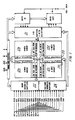
- FIG. 1 illustrates a semiconductor memory device with which the invention may be practiced.
- This exemplary device 10 is a DRAM of the so-called 16 Megabit size, having 224 or 16,777,216 one-transistor storage cells arranged in rows and columns.
- the device is partitioned into four identical logical data blocks 12, individually designated 12a, 12b, 12c and 12d.
- Each block 12 is of the four megabit size, comprising 4,194,304 memory cells arranged in an array of 4,096 rows and 1,024 columns C.
- each data block 12 is partitioned into sixteen sub-blocks 14.
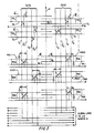
- the portion of a column C within each sub-block 14 is formed as a pair of interdigitated subcolumns SC. See Figure 3.
- 1024 pairs of subcolumns are in each sub-block.
- Banks of sense amplifiers SA border upper and lower opposing sides of each sub-block.
- the partial view of Figure 3 illustrates two adjacent pairs of interdigitated subcolumns SC.
- the first pair comprises subcolumns SC1 and SC2 and the second pair comprises subcolumns SC3 and SC4.
- Each of the pairs of subcolumns is associated with one of two adjacent columns in the sub-block.
- the subcolumns are arranged in a folded bitline configuration.
- each subcolumn SC comprises two bitline segments BL and BL , each containing memory cells and connected to the same sense amplifier SA.
- the two subcolumns within the sub-block 14 that are associated with the same column C are coupled to different sense amplifiers SA on opposing sides of the sub-block 14.
- each bank of sense amplifiers is shared by sub-columns in an adjacent pair of sub-blocks.
- each sub-block 14 there are 256 row or word lines R and 256 column select lines Y S .
- R and 256 column select lines Y S are shown in Figure 3.
- a row line is selectable based on row address information input to a one of sixteen row decoder stage 16 and a one of 256 row decoder stage 18. See Figure 2.
- column address decoders 20 turn on a select line Y S to control read/write data transfer for two columns.
- Path C I/O2 comprises two pairs of data lines D1, D 1 and D2, D 2, each pair providing one bit of information.
- path C I/O2 comprises two pairs of data lines D3, D 3 and D4, D 4.
- Lines D1, D2, D3 and D4 are connected to receive signals from bitline segments BL and lines D 1, D 2, D 3 and D 4, are connected to receive complementary signals from bitline segments BL .
- each pair of bitlines, in the four sub-columns of a sub-block that are associated with a particular select line Y S is paired to one of the data line pairs D i , D i .
- a four-bit wide global data path connects the local paths in each sub-block 14 of a logical data block 12 to the data I/O buffers 21.
- the row decoding arrangement enables simultaneous transfer of data to or from one sub-block 14 in each of the four data blocks 12 at a given time.
- the column select arrangement provides X 4 output from each data block 12.
- the I/O buffers 21 could provide 16 bit parallel I/O.
- row address signals RA0 through RA11 and column address signals CA0 through CA11 are input in conventional time-multiplexed manner being latched into row and column address buffers 22 and 24 according to timing signals RAS and CA S. See Figure 1.
- the first row decoder stage 16 selects one of the 16 sub-blocks in each of the data blocks 12.
- the second row decoder stage 18 selects one of the 256 rows within each selected sub-block based on the remaining 8 bits of row address information RA4 through RA11.
- the decoder circuitry 20 receives eight bits of column address data, A0 through A7, to provide a logic-high signal along one of the 256 select lines Y S in a data block 12.
- the data block provides four bits of data on a pair of 2-bit paths C I/O associated with the accessed sub-block.
- the next two bits of column address data CA8 and CA9 can be applied in any of several well known decoder circuit arrangements to vary the output of the data block from X 1 to X 4.
- each data block 12 includes, in addition to the 4,194,304 cells arranged along 1024 columns C, a predetermined number of redundant columns RC. Data I/O of the memory cells in each column RC is controlled by a redundant column select line.
- Y RS is illustrated in Figure 2.
- the number of redundant columns RC provided in each data block can be sufficient to maximize the yield of a production lot.
- it is desirable that individual data blocks in the device 10 comprise less than five redundant select lines Y RS .
- the redundant columns RC are formed as pairs of redundant sub-columns RSC and a redundant column select line Y RS is connected to access data from each column pair. All of the sub-blocks 14 in a data block 12 include the same number of redundant column selects.
- each pair of redundant columns can be wired to replace one or more portions of a pair of subcolumns in a column C.
- memory cells in each redundant column are arranged along the 4,096 rows of a data block 12 with each cell connected to a different row line so that all cells in a redundant column can be accessed with the row address decoder stages 16 and 18.
- each redundant select line Y RS enables data transfer between each of two constituent subcolumns RSC in a sub-block and a pair of data lines D i , D i associated with each of the paths C I/O1 and C I/O2 .
- a logic-high signal on redundant select Y RS1 connects each pair of folded bitline segments in the two selected redundant sub-columns RSC1 and RSC2 to the pairs of data lines D1, D 1 and D4, D 4.
- a logic high signal on select line Y RS1 will connect the bitline segments of RSC1 to data lines D1 and D 1 and will connect the bitline segments of RSC2 to data lines D4 and D 4.
- column repair decode circuitry can advantageously incorporate a level of row decoding in order to replace defective sections of columns C with equivalent sections of redundant columns RC.
- corresponding sections of columns C and redundant columns RC are responsive to the same level of row decoding.
- a comparator is programmed to replace a subcolumn pair, or a column segment of subcolumn pairs spanning multiple subblocks 14, with a corresponding section of a redundant column.
- Such segmentation is useful for allocating two or more portions of the same redundant column for repair of multiple defects occurring in different column segments, e.g., occurring in sections of memory having different column addresses.
- each pair of column sections which is to be replaced must be identifiable with different row address data.
- a different redundant column RC will be required to replace each of these. Otherwise, as long as sufficient row decoding is provided to associate each of the column sections which is to be replaced with a different section in the repair column, a single redundant column can be segmented to replace all column sections containing the defects in a data block 12.
- one redundant column RC can be used to eliminate defects occurring in multiple columns.
- the feature of decoding row address information in the column repair circuitry increases the number of repairs which can be made with a given number of redundant columns RC. For example, with a one of fifteen comparator decoder (receiving eight bits of column and three bits of row address information) any one of 8 segments in a redundant column RC can be programmed to replace any one of eight corresponding column segments in any of the four data blocks 12. Alternately, with a one of sixteen comparator decoder (receiving eight bits of column and four bits of row address information) the redundant columns RC can be segmented into sixteen sections each corresponding to a different pair of sub-columns SC in a different one of sixteen sub-blocks 14.
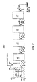
- the column repair decode circuitry includes a plurality of fusible comparator decoders 40.
- the decoder 40 shown schematically in Figure 4, will include a number of input circuits 41 each wired to receive an address signal and its complement.
- the decoder 40 includes n-x input circuits for receiving column address signals and m-y input circuits for receiving row address signals.
- the value of x corresponds to the number of columns C in a data block 12 and the value of y will depend on the desired level of segmentation.
- Each address input circuit 41 includes a fuse F for programming the decoder with the row or column address information needed to substitute one segment of memory cells along one redundant select line Y RS in a data block for a defective segment of memory cells in a column C of the same data block.
- the number of column repairs which can be made on the entire device 10 is equal in count to the total number of comparator decoders.
- any one of a predetermined number of sections within a repair column is addressable in the manner described above to replace a defective section along one of the 256 column select lines in any one of the four data blocks.
- a section in a redundant column is definable with a combination of row address information to replace a defective section in one of the data blocks.
- One of four data block select logic 42 includes a second stage of fusible decoders for identifying the data block to which each decoder 40 is to be dedicated.
- All of the second stage decoders in the logic block 42 include input circuits 41, like those of the decoders 40, receiving column address bits CA10 and CA11 to effect the one of four selection.
- the decoders of block 42 could provide a higher level of selection in order to allocate sections of the redundant columns RC to portions of the data blocks 12. For example, different redundant columns could be assigned to each half of each data block with the decoders in each group SS i wired to turn on the same redundant select line Y RS in each data half block. With this partitioning the second stage of decoders would include fusible circuits for dedicating each decoder 40 within each group SS i to a particular half block.
- the outputs of all the decoders 40 in each segment select group SS i are input to one of N select enable logic circuits 50.
- the select enable logic circuit 50 for that group outputs a logic high signal corresponding to the associated redundant select line Y RSi .
- each select enable logic circuit 50 provides a logic-high signal to one redundant select line Y RS in each data block.
- Figure 5 illustrates for two of the data blocks 12A and 12B combinatorial logic 52 for turning on one of N redundant select lines Y RS based on the output of the data block select logic 42 and the enable logic circuits 50.
- the repairability of a device containing a given number of random defects can be improved by increasing: the aggregate sum of redundant columns; the quantity of decoders to be provided for each redundant column; and the number of sections into which a column C is to be segmented for individual addressing.
- a higher level of repair can be achieved with fewer redundant columns.
- the likelihood of device repairability will be improved by increasing the level of decoding as well as the number of decoders associated with each redundant column select line Y RS .
- Figures 6A through 6E portray an analysis and methodology for improving the level of defect repair for one data block 12 of the device 10. Given a fixed pattern of five defects each figure depicts an exemplary number of individually addressable sections into which a column C can be segmented to effect replacement with a redundant column RC. For simplicity it is assumed that each defect occurs along a different column select line Y S and in a different one of sixteen sub-blocks 14. For each of the five examples illustrated in Figures 6, as many as five redundant select lines Y RS are available to effect repairs.
- each comparator decoder When no row decoding is incorporated in each comparator decoders ( Figure 6A) the number of decoders in each segment select group SS i degenerates to one decoder per redundant select line Y RS .
- the comparator decoders include no row decode circuitry the columns C cannot be segmented into subsections for individual replacement. Therefore all five redundant select lines must be allocated for repair of the five column defects.
- the columns can be segmented in two sections (each section covering eight of the sub-blocks 14) and the segment select groups SS i can include a maximum of two decoders per select line.
- Full repair is implemented with four select lines Y RS and five decoders.
- the comparator decoders perform two bits of row decoding ( Figure 6C) the columns are segmented into four sections (each section covering four of the sub-blocks 14) and the segment select groups SS i each include up to three decoders. With the scheme of Figure 6C three select lines Y RS and five decoders will effect full repair of the data block 12.
- Provision of three row address bits to the comparator decoders segments the columns into eight sections ( Figure 6D) and permits four decoders per select line Y RS . Repair of all five defects will be realized with only two select lines Y RS wherein at least one segment select group SS i includes four decoders.
- the comparator decoders can resolve the columns into sixteen sections (each corresponding to one sub-block 14) with four bits of row address information. When one segment select group includes five comparator decoders all five repairs can be performed with one select line Y RS .
- Figures 7A through 7F illustrate trends in probability of complete repair for various device defect levels as the level of row decoding in the comparator decoders increases from zero to four bits.
- the numbers in brackets, e.g., [2] [2], above each graph indicate the number of decoders 40 assigned to each segment select group SS i .
- a bracketed number is provided for each segment select group.
- Figure 7A illustrates improvements in repairability (as a function of row address inputs to the decoders 40) for an embodiment having two segment select groups and two decoders 40 per segment select group.
- Figure 7B suggests that for the embodiment of three segment select groups, each including two decoders 40, repairability may not improve with a higher degree of segmentation.
- Figures 7D through 7F indicate improved repairability with higher levels of segmentation. The figures illustrate that repairability according to the invention is dependent on device architecture and improvements may not always be obtained. Comparison of Figures 7A, 7D and 7F suggests that device repairability improves as the number of decoders 40 per segment select group and the level of decoding both increase.
- a repair scheme for the entire device could comprise two redundant select lines Y RS each coupled to a different one of two segment select groups SS i .
- the groups SS i would comprise four decoders 40 with all of the decoders receiving four bits of row address information to segment each redundant column into sixteen sections.
- a satisfactory level of repairability may be achievable with other combinations, e.g., three decoders per segment select group SS i with each decoder receiving three bits of row address information.
- the selection of two different repair schemes which exhibit comparable levels of repairability may be based in part on space constraints.
- the determination of an acceptable level of repair should be made in view of yield projections as well as space constraints to avoid over design.
- space constraints and other economies are not critical factors the device can simple incorporate a sufficient number of decoders uniformly distributed among the segment select groups to assure ample repairability.
- a method of maximizing repair efficiency with a given number of redundant select lines in each data block involves assigning multiple decoders to each of the redundant select lines so that each line is capable of replacing multiple defective column portions with redundant column portions that are coupled to the same select line.
- section , portion and segment as used herein with regard to a column C or a redundant column RC, each comprehend less than a full column of memory cells and fewer than all of the memory cells connected along one column select line.
- section , portion and segment define less than a full row of memory cells or fewer than all of the memory cells along a particular row line.
- redundancy schemes can be optimized for space efficiency as well as repairability.
- the desirability of minimizing the geometric size of a redundancy scheme stems from the space consuming nature of fuses which are used to program the decoders 40.
- fuse lines for redundant decoders are significantly wider, e.g., one to two microns on center.
- layouts have spaced fuse lines seven microns on center from adjacent fuse lines or other conductors.
- corresponding sections in the other data blocks could also be replaced by redundant sections that are coupled to the same decoder.
- replacement of a column section along one data block could require replacement of all corresponding column sections in the other data blocks.
- a redundant column section in each of several different data blocks shares a common redundant decoder, the assignment of one of those redundant column sections to a specific address constrains assignment of the other redundant column sections in the other data blocks to the same address. With this address dedication scheme the usefulness of a redundant column section in a particular data block which could otherwise be used to replace a defective column section may appear lost.
- the efficiency of column repair can be further improved upon by incorporating additional information within the comparator decoders, e.g., data block designation, to further define where a defect is located and dedicate a portion of only one redundant column each time a decoder is programmed.
- additional information within the comparator decoders e.g., data block designation
- a segment of a redundant will not be used to replace a good segment of a column C. Rather, an addressed segment of a redundant column will be activated only when the corresponding defective segment of a single column, i.e., in only one data block, is addressed.
- the comparator decoders 40 of Figures 4 and 5 would include additional fusing and address inputs in order to respond to two bits of data block address information (CA10, CA11).
- CA10, CA11 data block address information
- modification repair segments located in different data blocks comprising redundant subcolumns connected to the same select line Y RS and identifiable with the same row address information, can be assigned different column address information so that each may be used to replace a defective column portion having a different column address, i.e., A0 through A7.
Landscapes
- For Increasing The Reliability Of Semiconductor Memories (AREA)
- Dram (AREA)
- Design And Manufacture Of Integrated Circuits (AREA)
Applications Claiming Priority (2)
| Application Number | Priority Date | Filing Date | Title |
|---|---|---|---|
| US479510 | 1990-02-14 | ||
| US07/479,510 US5126973A (en) | 1990-02-14 | 1990-02-14 | Redundancy scheme for eliminating defects in a memory device |
Publications (3)
| Publication Number | Publication Date |
|---|---|
| EP0442319A2 true EP0442319A2 (de) | 1991-08-21 |
| EP0442319A3 EP0442319A3 (en) | 1992-10-14 |
| EP0442319B1 EP0442319B1 (de) | 2005-03-30 |
Family
ID=23904328
Family Applications (1)
| Application Number | Title | Priority Date | Filing Date |
|---|---|---|---|
| EP91101121A Expired - Lifetime EP0442319B1 (de) | 1990-02-14 | 1991-01-29 | Redundanz-Aufstellung zur Beseitigung von Defekten in einer Speicheranordnung |
Country Status (5)
| Country | Link |
|---|---|
| US (1) | US5126973A (de) |
| EP (1) | EP0442319B1 (de) |
| KR (1) | KR100227987B1 (de) |
| CN (1) | CN1039606C (de) |
| DE (1) | DE69133450T2 (de) |
Cited By (3)
| Publication number | Priority date | Publication date | Assignee | Title |
|---|---|---|---|---|
| GB2258066A (en) * | 1991-07-26 | 1993-01-27 | Samsung Electronics Co Ltd | Semiconductor memory redunduncy |
| WO1996031825A1 (en) * | 1995-04-04 | 1996-10-10 | Memory Corporation Plc | Memory management |
| EP0890902A2 (de) * | 1997-07-10 | 1999-01-13 | Siemens Aktiengesellschaft | Redundanzschaltung für Halbleiterspeicher |
Families Citing this family (63)
| Publication number | Priority date | Publication date | Assignee | Title |
|---|---|---|---|---|
| EP0392895B1 (de) | 1989-04-13 | 1995-12-13 | Sundisk Corporation | EEprom-System mit Blocklöschung |
| US5398206A (en) * | 1990-03-02 | 1995-03-14 | Hitachi, Ltd. | Semiconductor memory device with data error compensation |
| GB9007796D0 (en) * | 1990-04-06 | 1990-06-06 | Foss Richard C | Dynamic memory row/column redundancy scheme |
| US5287311A (en) * | 1991-05-31 | 1994-02-15 | Texas Instruments Incorporated | Method and apparatus for implementing ×2 parity DRAM for 16 bit systems from ×4 parity DRAM |
| US5392247A (en) * | 1991-09-19 | 1995-02-21 | Mitsubishi Denki Kabushiki Kaisha | Semiconductor memory device including redundancy circuit |
| US6781895B1 (en) | 1991-12-19 | 2004-08-24 | Kabushiki Kaisha Toshiba | Non-volatile semiconductor memory device and memory system using the same |
| US5361227A (en) * | 1991-12-19 | 1994-11-01 | Kabushiki Kaisha Toshiba | Non-volatile semiconductor memory device and memory system using the same |
| US5295101A (en) * | 1992-01-31 | 1994-03-15 | Texas Instruments Incorporated | Array block level redundancy with steering logic |
| JP2730375B2 (ja) * | 1992-01-31 | 1998-03-25 | 日本電気株式会社 | 半導体メモリ |
| JP3040625B2 (ja) * | 1992-02-07 | 2000-05-15 | 松下電器産業株式会社 | 半導体記憶装置 |
| US5268866A (en) * | 1992-03-02 | 1993-12-07 | Motorola, Inc. | Memory with column redundancy and localized column redundancy control signals |
| WO1994007242A1 (en) * | 1992-09-21 | 1994-03-31 | Atmel Corporation | High speed redundant memory |
| JPH0831573B2 (ja) * | 1992-10-01 | 1996-03-27 | 日本電気株式会社 | ダイナミックram |
| JP3212421B2 (ja) * | 1993-09-20 | 2001-09-25 | 富士通株式会社 | 不揮発性半導体記憶装置 |
| US5495447A (en) * | 1993-10-08 | 1996-02-27 | Digital Equipment Corporation | Method and apparatus using mapped redundancy to perform multiple large block memory array repair |
| US5539696A (en) * | 1994-01-31 | 1996-07-23 | Patel; Vipul C. | Method and apparatus for writing data in a synchronous memory having column independent sections and a method and apparatus for performing write mask operations |
| KR970003337B1 (ko) * | 1994-07-07 | 1997-03-17 | 현대전자산업 주식회사 | 데이타 버스 라인 부하 감소 장치를 포함한 메모리 소자 |
| JP3421441B2 (ja) * | 1994-09-22 | 2003-06-30 | 東芝マイクロエレクトロニクス株式会社 | ダイナミック型メモリ |
| JPH08129876A (ja) * | 1994-10-28 | 1996-05-21 | Nec Corp | 半導体記憶装置 |
| US5691945A (en) * | 1995-05-31 | 1997-11-25 | Macronix International Co., Ltd. | Technique for reconfiguring a high density memory |
| US5668763A (en) * | 1996-02-26 | 1997-09-16 | Fujitsu Limited | Semiconductor memory for increasing the number of half good memories by selecting and using good memory blocks |
| JPH09288888A (ja) * | 1996-04-22 | 1997-11-04 | Mitsubishi Electric Corp | 半導体記憶装置 |
| US5841710A (en) * | 1997-02-14 | 1998-11-24 | Micron Electronics, Inc. | Dynamic address remapping decoder |
| US6314527B1 (en) | 1998-03-05 | 2001-11-06 | Micron Technology, Inc. | Recovery of useful areas of partially defective synchronous memory components |
| US6332183B1 (en) | 1998-03-05 | 2001-12-18 | Micron Technology, Inc. | Method for recovery of useful areas of partially defective synchronous memory components |
| US6381708B1 (en) | 1998-04-28 | 2002-04-30 | Micron Technology, Inc. | Method for decoding addresses for a defective memory array |
| US6381707B1 (en) | 1998-04-28 | 2002-04-30 | Micron Technology, Inc. | System for decoding addresses for a defective memory array |
| US6295231B1 (en) * | 1998-07-17 | 2001-09-25 | Kabushiki Kaisha Toshiba | High-speed cycle clock-synchronous memory device |
| US6496876B1 (en) | 1998-12-21 | 2002-12-17 | Micron Technology, Inc. | System and method for storing a tag to identify a functional storage location in a memory device |
| US6163495A (en) * | 1999-09-17 | 2000-12-19 | Cypress Semiconductor Corp. | Architecture, method(s) and circuitry for low power memories |
| US6530045B1 (en) * | 1999-12-03 | 2003-03-04 | Micron Technology, Inc. | Apparatus and method for testing rambus DRAMs |
| US6578157B1 (en) | 2000-03-06 | 2003-06-10 | Micron Technology, Inc. | Method and apparatus for recovery of useful areas of partially defective direct rambus rimm components |
| US7269765B1 (en) * | 2000-04-13 | 2007-09-11 | Micron Technology, Inc. | Method and apparatus for storing failing part locations in a module |
| US6314030B1 (en) * | 2000-06-14 | 2001-11-06 | Micron Technology, Inc. | Semiconductor memory having segmented row repair |
| US20030235089A1 (en) * | 2002-04-02 | 2003-12-25 | Gerhard Mueller | Memory array with diagonal bitlines |
| US6809972B2 (en) * | 2003-03-13 | 2004-10-26 | Infineon Technologies Ag | Circuit technique for column redundancy fuse latches |
| US7350132B2 (en) * | 2003-09-10 | 2008-03-25 | Hewlett-Packard Development Company, L.P. | Nanoscale interconnection interface |
| US20050073875A1 (en) * | 2003-10-03 | 2005-04-07 | Matsushita Electric Industrial Co., Ltd. | Redundancy repaired yield calculation method |
| KR100724567B1 (ko) * | 2005-08-05 | 2007-06-04 | 삼성전자주식회사 | 반도체 메모리 장치 |
| US7292487B1 (en) | 2006-05-10 | 2007-11-06 | Micron Technology, Inc. | Independent polling for multi-page programming |
| US8878860B2 (en) * | 2006-12-28 | 2014-11-04 | Intel Corporation | Accessing memory using multi-tiling |
| US20120075943A1 (en) * | 2010-09-29 | 2012-03-29 | Macronix International Co., Ltd. | Method and Apparatus for Memory Repair With Redundant Columns |
| TWI482168B (zh) * | 2010-10-08 | 2015-04-21 | Macronix Int Co Ltd | 具有備援行之記憶體修復的方法及裝置 |
| CN102456414B (zh) * | 2010-10-20 | 2014-11-26 | 旺宏电子股份有限公司 | 具有备援行的存储器装置及其修复方法 |
| KR101211042B1 (ko) * | 2010-11-23 | 2012-12-13 | 에스케이하이닉스 주식회사 | 고장 정보 저장장치 및 저장방법 |
| KR101133689B1 (ko) * | 2010-11-23 | 2012-04-24 | 에스케이하이닉스 주식회사 | 리페어 분석 장치 및 방법 |
| CN102157206A (zh) * | 2011-01-17 | 2011-08-17 | 上海宏力半导体制造有限公司 | 具有冗余电路的存储器以及为存储器提供冗余电路的方法 |
| KR20120122594A (ko) * | 2011-04-29 | 2012-11-07 | 에스케이하이닉스 주식회사 | 반도체 장치 |
| US8976604B2 (en) | 2012-02-13 | 2015-03-10 | Macronix International Co., Lt. | Method and apparatus for copying data with a memory array having redundant memory |
| US9165680B2 (en) | 2013-03-11 | 2015-10-20 | Macronix International Co., Ltd. | Memory integrated circuit with a page register/status memory capable of storing only a subset of row blocks of main column blocks |
| US9305664B2 (en) | 2014-03-26 | 2016-04-05 | Texas Instruments Incorporated | Memory repair categorization tracking |
| KR20160056586A (ko) * | 2014-11-12 | 2016-05-20 | 에스케이하이닉스 주식회사 | 리페어 회로 및 이를 포함하는 반도체 메모리 장치 |
| US9773571B2 (en) | 2014-12-16 | 2017-09-26 | Macronix International Co., Ltd. | Memory repair redundancy with array cache redundancy |
| US20160218286A1 (en) | 2015-01-23 | 2016-07-28 | Macronix International Co., Ltd. | Capped contact structure with variable adhesion layer thickness |
| US9514815B1 (en) | 2015-05-13 | 2016-12-06 | Macronix International Co., Ltd. | Verify scheme for ReRAM |
| US10108509B2 (en) * | 2015-07-16 | 2018-10-23 | Texas Instruments Incorporated | Dynamic enabling of redundant memory cells during operating life |
| KR20170055222A (ko) | 2015-11-11 | 2017-05-19 | 삼성전자주식회사 | 리페어 단위 변경 기능을 가지는 메모리 장치 및 메모리 시스템 |
| US9691478B1 (en) | 2016-04-22 | 2017-06-27 | Macronix International Co., Ltd. | ReRAM array configuration for bipolar operation |
| US9959928B1 (en) | 2016-12-13 | 2018-05-01 | Macronix International Co., Ltd. | Iterative method and apparatus to program a programmable resistance memory element using stabilizing pulses |
| US10971247B2 (en) * | 2018-03-29 | 2021-04-06 | Samsung Electronics Co., Ltd. | Semiconductor memory devices, memory systems, and methods of operating semiconductor memory devices |
| US11646095B2 (en) * | 2020-03-06 | 2023-05-09 | Micron Technology, Inc. | Configurable soft post-package repair (SPPR) schemes |
| US11815995B1 (en) * | 2022-04-27 | 2023-11-14 | Macronix International Co., Ltd. | Redundancy schemes for repairing column defects |
| CN116072207B (zh) * | 2023-04-06 | 2023-08-08 | 长鑫存储技术有限公司 | 故障寻址电路及存储器 |
Citations (3)
| Publication number | Priority date | Publication date | Assignee | Title |
|---|---|---|---|---|
| EP0180212A2 (de) * | 1980-10-06 | 1986-05-07 | THORN EMI North America Inc. | Redundanzstruktur für einen dynamischen Speicher |
| FR2611301A1 (fr) * | 1987-02-24 | 1988-08-26 | Thomson Semiconducteurs | Memoire integree avec redondance de colonnes de donnees |
| US4837747A (en) * | 1986-11-29 | 1989-06-06 | Mitsubishi Denki Kabushiki Kaisha | Redundary circuit with a spare main decoder responsive to an address of a defective cell in a selected cell block |
Family Cites Families (3)
| Publication number | Priority date | Publication date | Assignee | Title |
|---|---|---|---|---|
| US4047163A (en) * | 1975-07-03 | 1977-09-06 | Texas Instruments Incorporated | Fault-tolerant cell addressable array |
| JPS59144098A (ja) * | 1983-02-08 | 1984-08-17 | Fujitsu Ltd | 半導体記憶装置 |
| US4754434A (en) * | 1985-08-28 | 1988-06-28 | Advanced Micro Devices, Inc. | Switching plane redundancy |
-
1990
- 1990-02-14 US US07/479,510 patent/US5126973A/en not_active Expired - Lifetime
-
1991
- 1991-01-29 DE DE69133450T patent/DE69133450T2/de not_active Expired - Lifetime
- 1991-01-29 EP EP91101121A patent/EP0442319B1/de not_active Expired - Lifetime
- 1991-02-13 CN CN91101028A patent/CN1039606C/zh not_active Expired - Lifetime
- 1991-02-13 KR KR1019910002550A patent/KR100227987B1/ko not_active IP Right Cessation
Patent Citations (3)
| Publication number | Priority date | Publication date | Assignee | Title |
|---|---|---|---|---|
| EP0180212A2 (de) * | 1980-10-06 | 1986-05-07 | THORN EMI North America Inc. | Redundanzstruktur für einen dynamischen Speicher |
| US4837747A (en) * | 1986-11-29 | 1989-06-06 | Mitsubishi Denki Kabushiki Kaisha | Redundary circuit with a spare main decoder responsive to an address of a defective cell in a selected cell block |
| FR2611301A1 (fr) * | 1987-02-24 | 1988-08-26 | Thomson Semiconducteurs | Memoire integree avec redondance de colonnes de donnees |
Cited By (8)
| Publication number | Priority date | Publication date | Assignee | Title |
|---|---|---|---|---|
| GB2258066A (en) * | 1991-07-26 | 1993-01-27 | Samsung Electronics Co Ltd | Semiconductor memory redunduncy |
| WO1996031825A1 (en) * | 1995-04-04 | 1996-10-10 | Memory Corporation Plc | Memory management |
| US6065090A (en) * | 1995-04-04 | 2000-05-16 | Memory Corporation Plc | Memory management apparatus that replaces defective storage locations with functional storage locations |
| KR100352910B1 (ko) * | 1995-04-04 | 2002-12-16 | 스마트에이에스아이씨 테크날러지 인코퍼레이티드 | 메모리의결함위치를작동위치로대체하기위한메모리관리장치 |
| EP0890902A2 (de) * | 1997-07-10 | 1999-01-13 | Siemens Aktiengesellschaft | Redundanzschaltung für Halbleiterspeicher |
| EP0890902A3 (de) * | 1997-07-10 | 1999-09-22 | Siemens Aktiengesellschaft | Redundanzschaltung für Halbleiterspeicher |
| US6188617B1 (en) | 1997-07-10 | 2001-02-13 | Infineon Technologies Ag | Reundancy circuit for semiconductor memories |
| KR100325649B1 (ko) * | 1997-07-10 | 2002-05-09 | 칼 하인쯔 호르닝어 | 반도체메모리용용장회로 |
Also Published As
| Publication number | Publication date |
|---|---|
| DE69133450T2 (de) | 2006-02-09 |
| DE69133450D1 (de) | 2005-05-04 |
| KR100227987B1 (ko) | 1999-11-01 |
| KR910016009A (ko) | 1991-09-30 |
| EP0442319B1 (de) | 2005-03-30 |
| EP0442319A3 (en) | 1992-10-14 |
| CN1056360A (zh) | 1991-11-20 |
| CN1039606C (zh) | 1998-08-26 |
| US5126973A (en) | 1992-06-30 |
Similar Documents
| Publication | Publication Date | Title |
|---|---|---|
| US5126973A (en) | Redundancy scheme for eliminating defects in a memory device | |
| US5270975A (en) | Memory device having a non-uniform redundancy decoder arrangement | |
| US5295101A (en) | Array block level redundancy with steering logic | |
| US6910152B2 (en) | Device and method for repairing a semiconductor memory | |
| US8713374B2 (en) | Memory device and method for repairing a semiconductor memory | |
| US6560728B2 (en) | Layout for semiconductor memory device having a plurality of rows and columns of circuit cells divided into first and second planes that are not simultaneously active | |
| US5163023A (en) | Memory circuit capable of replacing a faulty column with a spare column | |
| JP3180905B2 (ja) | リペア可能な半導体メモリアレーおよびリペア可能な半導体メモリアレーの製造方法 | |
| US5255228A (en) | Semiconductor memory device with redundancy circuits | |
| JP2004503897A (ja) | 行修理をセグメント化した半導体メモリ | |
| US6490210B2 (en) | Semiconductor memory integrated circuit employing a redundant circuit system for compensating for defectiveness | |
| US4691300A (en) | Redundant column substitution architecture with improved column access time | |
| US6295595B1 (en) | Method and structure for accessing a reduced address space of a defective memory | |
| US6208569B1 (en) | Method of and apparatus for sharing redundancy circuits between memory arrays within a semiconductor memory device | |
| JP2004062999A (ja) | 半導体記憶装置 | |
| JPH04222998A (ja) | 半導体メモリ装置 | |
| EP0448980B1 (de) | Vorrichtung und Verfahren für die Beseitigung von Fehlern eines Speichers | |
| US5982680A (en) | Semiconductor memory | |
| JPH0684392A (ja) | メモリ装置内の欠陥を消去する冗長方式 | |
| JP2900944B2 (ja) | 半導体メモリ | |
| KR100546176B1 (ko) | 리던던시 회로 | |
| WO1998028746A1 (en) | Redundancy for wide hierarchical i/o organizations | |
| KR20030084029A (ko) | 플렉서블 리던던스 체계를 갖는 반도체 메모리 장치 |
Legal Events
| Date | Code | Title | Description |
|---|---|---|---|
| PUAI | Public reference made under article 153(3) epc to a published international application that has entered the european phase |
Free format text: ORIGINAL CODE: 0009012 |
|
| AK | Designated contracting states |
Kind code of ref document: A2 Designated state(s): DE FR GB IT NL |
|
| PUAL | Search report despatched |
Free format text: ORIGINAL CODE: 0009013 |
|
| AK | Designated contracting states |
Kind code of ref document: A3 Designated state(s): DE FR GB IT NL |
|
| 17P | Request for examination filed |
Effective date: 19930312 |
|
| 17Q | First examination report despatched |
Effective date: 19951123 |
|
| GRAP | Despatch of communication of intention to grant a patent |
Free format text: ORIGINAL CODE: EPIDOSNIGR1 |
|
| GRAS | Grant fee paid |
Free format text: ORIGINAL CODE: EPIDOSNIGR3 |
|
| GRAA | (expected) grant |
Free format text: ORIGINAL CODE: 0009210 |
|
| AK | Designated contracting states |
Kind code of ref document: B1 Designated state(s): DE FR GB IT NL |
|
| PG25 | Lapsed in a contracting state [announced via postgrant information from national office to epo] |
Ref country code: IT Free format text: LAPSE BECAUSE OF FAILURE TO SUBMIT A TRANSLATION OF THE DESCRIPTION OR TO PAY THE FEE WITHIN THE PRE;WARNING: LAPSES OF ITALIAN PATENTS WITH EFFECTIVE DATE BEFORE 2007 MAY HAVE OCCURRED AT ANY TIME BEFORE 2007. THE CORRECT EFFECTIVE DATE MAY BE DIFFERENT FROM THE ONE RECORDED.SCRIBED TIME-LIMIT Effective date: 20050330 Ref country code: NL Free format text: LAPSE BECAUSE OF FAILURE TO SUBMIT A TRANSLATION OF THE DESCRIPTION OR TO PAY THE FEE WITHIN THE PRESCRIBED TIME-LIMIT Effective date: 20050330 |
|
| REG | Reference to a national code |
Ref country code: GB Ref legal event code: FG4D |
|
| REF | Corresponds to: |
Ref document number: 69133450 Country of ref document: DE Date of ref document: 20050504 Kind code of ref document: P |
|
| NLV1 | Nl: lapsed or annulled due to failure to fulfill the requirements of art. 29p and 29m of the patents act | ||
| ET | Fr: translation filed | ||
| PLBI | Opposition filed |
Free format text: ORIGINAL CODE: 0009260 |
|
| PLAZ | Examination of admissibility of opposition: despatch of communication + time limit |
Free format text: ORIGINAL CODE: EPIDOSNOPE2 |
|
| 26 | Opposition filed |
Opponent name: INFINEON TECHNOLOGIES AG Effective date: 20051229 |
|
| PLAX | Notice of opposition and request to file observation + time limit sent |
Free format text: ORIGINAL CODE: EPIDOSNOBS2 |
|
| PLBA | Examination of admissibility of opposition: reply received |
Free format text: ORIGINAL CODE: EPIDOSNOPE4 |
|
| PLAF | Information modified related to communication of a notice of opposition and request to file observations + time limit |
Free format text: ORIGINAL CODE: EPIDOSCOBS2 |
|
| PLBB | Reply of patent proprietor to notice(s) of opposition received |
Free format text: ORIGINAL CODE: EPIDOSNOBS3 |
|
| PLBP | Opposition withdrawn |
Free format text: ORIGINAL CODE: 0009264 |
|
| PLBD | Termination of opposition procedure: decision despatched |
Free format text: ORIGINAL CODE: EPIDOSNOPC1 |
|
| PLBM | Termination of opposition procedure: date of legal effect published |
Free format text: ORIGINAL CODE: 0009276 |
|
| STAA | Information on the status of an ep patent application or granted ep patent |
Free format text: STATUS: OPPOSITION PROCEDURE CLOSED |
|
| 27C | Opposition proceedings terminated |
Effective date: 20070301 |
|
| PLAB | Opposition data, opponent's data or that of the opponent's representative modified |
Free format text: ORIGINAL CODE: 0009299OPPO |
|
| PGFP | Annual fee paid to national office [announced via postgrant information from national office to epo] |
Ref country code: GB Payment date: 20091211 Year of fee payment: 20 |
|
| PGFP | Annual fee paid to national office [announced via postgrant information from national office to epo] |
Ref country code: FR Payment date: 20100125 Year of fee payment: 20 |
|
| PGFP | Annual fee paid to national office [announced via postgrant information from national office to epo] |
Ref country code: DE Payment date: 20100129 Year of fee payment: 20 |
|
| REG | Reference to a national code |
Ref country code: GB Ref legal event code: PE20 Expiry date: 20110128 |
|
| PG25 | Lapsed in a contracting state [announced via postgrant information from national office to epo] |
Ref country code: GB Free format text: LAPSE BECAUSE OF EXPIRATION OF PROTECTION Effective date: 20110128 |
|
| PG25 | Lapsed in a contracting state [announced via postgrant information from national office to epo] |
Ref country code: DE Free format text: LAPSE BECAUSE OF EXPIRATION OF PROTECTION Effective date: 20110129 |