EP0417738A1 - Dispositif semi-conducteur de puissance - Google Patents
Dispositif semi-conducteur de puissance Download PDFInfo
- Publication number
- EP0417738A1 EP0417738A1 EP90117501A EP90117501A EP0417738A1 EP 0417738 A1 EP0417738 A1 EP 0417738A1 EP 90117501 A EP90117501 A EP 90117501A EP 90117501 A EP90117501 A EP 90117501A EP 0417738 A1 EP0417738 A1 EP 0417738A1
- Authority
- EP
- European Patent Office
- Prior art keywords
- region
- type
- life time
- depth
- layer
- Prior art date
- Legal status (The legal status is an assumption and is not a legal conclusion. Google has not performed a legal analysis and makes no representation as to the accuracy of the status listed.)
- Granted
Links
- 239000004065 semiconductor Substances 0.000 title claims abstract description 37
- 239000012535 impurity Substances 0.000 claims abstract description 30
- 238000010894 electron beam technology Methods 0.000 claims description 5
- 230000002285 radioactive effect Effects 0.000 claims description 4
- 238000009826 distribution Methods 0.000 abstract description 7
- 230000004807 localization Effects 0.000 abstract description 5
- 230000003071 parasitic effect Effects 0.000 description 22
- 238000009792 diffusion process Methods 0.000 description 13
- 229910021420 polycrystalline silicon Inorganic materials 0.000 description 13
- 229920005591 polysilicon Polymers 0.000 description 12
- XUIMIQQOPSSXEZ-UHFFFAOYSA-N Silicon Chemical compound [Si] XUIMIQQOPSSXEZ-UHFFFAOYSA-N 0.000 description 11
- 230000000694 effects Effects 0.000 description 11
- 229910052710 silicon Inorganic materials 0.000 description 11
- 239000010703 silicon Substances 0.000 description 11
- 230000015556 catabolic process Effects 0.000 description 10
- 238000000034 method Methods 0.000 description 9
- 238000012986 modification Methods 0.000 description 9
- 230000004048 modification Effects 0.000 description 9
- 239000000969 carrier Substances 0.000 description 7
- 239000000758 substrate Substances 0.000 description 7
- 210000000746 body region Anatomy 0.000 description 6
- 230000003247 decreasing effect Effects 0.000 description 6
- 230000005684 electric field Effects 0.000 description 6
- PCHJSUWPFVWCPO-UHFFFAOYSA-N gold Chemical compound [Au] PCHJSUWPFVWCPO-UHFFFAOYSA-N 0.000 description 6
- 229910052737 gold Inorganic materials 0.000 description 6
- 239000010931 gold Substances 0.000 description 6
- BASFCYQUMIYNBI-UHFFFAOYSA-N platinum Chemical compound [Pt] BASFCYQUMIYNBI-UHFFFAOYSA-N 0.000 description 6
- 229910001385 heavy metal Inorganic materials 0.000 description 5
- 229910052751 metal Inorganic materials 0.000 description 5
- 239000002184 metal Substances 0.000 description 5
- 230000000875 corresponding effect Effects 0.000 description 4
- 230000006798 recombination Effects 0.000 description 4
- 238000011161 development Methods 0.000 description 3
- 238000004519 manufacturing process Methods 0.000 description 3
- 229910052697 platinum Inorganic materials 0.000 description 3
- 238000006731 degradation reaction Methods 0.000 description 2
- 229910052698 phosphorus Inorganic materials 0.000 description 2
- 239000011574 phosphorus Substances 0.000 description 2
- -1 phosphorus ions Chemical class 0.000 description 2
- 238000004904 shortening Methods 0.000 description 2
- 229910052782 aluminium Inorganic materials 0.000 description 1
- XAGFODPZIPBFFR-UHFFFAOYSA-N aluminium Chemical compound [Al] XAGFODPZIPBFFR-UHFFFAOYSA-N 0.000 description 1
- 238000004458 analytical method Methods 0.000 description 1
- 229910052785 arsenic Inorganic materials 0.000 description 1
- RQNWIZPPADIBDY-UHFFFAOYSA-N arsenic atom Chemical compound [As] RQNWIZPPADIBDY-UHFFFAOYSA-N 0.000 description 1
- 238000004364 calculation method Methods 0.000 description 1
- 239000002131 composite material Substances 0.000 description 1
- 230000001276 controlling effect Effects 0.000 description 1
- 238000007796 conventional method Methods 0.000 description 1
- 238000013461 design Methods 0.000 description 1
- 238000011156 evaluation Methods 0.000 description 1
- 230000005669 field effect Effects 0.000 description 1
- 238000002513 implantation Methods 0.000 description 1
- 238000005468 ion implantation Methods 0.000 description 1
- 150000002500 ions Chemical class 0.000 description 1
- 229910044991 metal oxide Inorganic materials 0.000 description 1
- 150000004706 metal oxides Chemical class 0.000 description 1
- 239000002245 particle Substances 0.000 description 1
- 238000001259 photo etching Methods 0.000 description 1
- 238000005215 recombination Methods 0.000 description 1
- 229920006395 saturated elastomer Polymers 0.000 description 1
- 238000005204 segregation Methods 0.000 description 1
Images


Classifications
-
- H—ELECTRICITY
- H01—ELECTRIC ELEMENTS
- H01L—SEMICONDUCTOR DEVICES NOT COVERED BY CLASS H10
- H01L29/00—Semiconductor devices specially adapted for rectifying, amplifying, oscillating or switching and having potential barriers; Capacitors or resistors having potential barriers, e.g. a PN-junction depletion layer or carrier concentration layer; Details of semiconductor bodies or of electrodes thereof ; Multistep manufacturing processes therefor
- H01L29/66—Types of semiconductor device ; Multistep manufacturing processes therefor
- H01L29/68—Types of semiconductor device ; Multistep manufacturing processes therefor controllable by only the electric current supplied, or only the electric potential applied, to an electrode which does not carry the current to be rectified, amplified or switched
- H01L29/76—Unipolar devices, e.g. field effect transistors
- H01L29/772—Field effect transistors
- H01L29/78—Field effect transistors with field effect produced by an insulated gate
-
- H—ELECTRICITY
- H01—ELECTRIC ELEMENTS
- H01L—SEMICONDUCTOR DEVICES NOT COVERED BY CLASS H10
- H01L29/00—Semiconductor devices specially adapted for rectifying, amplifying, oscillating or switching and having potential barriers; Capacitors or resistors having potential barriers, e.g. a PN-junction depletion layer or carrier concentration layer; Details of semiconductor bodies or of electrodes thereof ; Multistep manufacturing processes therefor
- H01L29/66—Types of semiconductor device ; Multistep manufacturing processes therefor
- H01L29/68—Types of semiconductor device ; Multistep manufacturing processes therefor controllable by only the electric current supplied, or only the electric potential applied, to an electrode which does not carry the current to be rectified, amplified or switched
- H01L29/70—Bipolar devices
- H01L29/72—Transistor-type devices, i.e. able to continuously respond to applied control signals
- H01L29/739—Transistor-type devices, i.e. able to continuously respond to applied control signals controlled by field-effect, e.g. bipolar static induction transistors [BSIT]
- H01L29/7393—Insulated gate bipolar mode transistors, i.e. IGBT; IGT; COMFET
- H01L29/7395—Vertical transistors, e.g. vertical IGBT
-
- H—ELECTRICITY
- H01—ELECTRIC ELEMENTS
- H01L—SEMICONDUCTOR DEVICES NOT COVERED BY CLASS H10
- H01L29/00—Semiconductor devices specially adapted for rectifying, amplifying, oscillating or switching and having potential barriers; Capacitors or resistors having potential barriers, e.g. a PN-junction depletion layer or carrier concentration layer; Details of semiconductor bodies or of electrodes thereof ; Multistep manufacturing processes therefor
- H01L29/02—Semiconductor bodies ; Multistep manufacturing processes therefor
- H01L29/06—Semiconductor bodies ; Multistep manufacturing processes therefor characterised by their shape; characterised by the shapes, relative sizes, or dispositions of the semiconductor regions ; characterised by the concentration or distribution of impurities within semiconductor regions
- H01L29/0684—Semiconductor bodies ; Multistep manufacturing processes therefor characterised by their shape; characterised by the shapes, relative sizes, or dispositions of the semiconductor regions ; characterised by the concentration or distribution of impurities within semiconductor regions characterised by the shape, relative sizes or dispositions of the semiconductor regions or junctions between the regions
- H01L29/0692—Surface layout
- H01L29/0696—Surface layout of cellular field-effect devices, e.g. multicellular DMOS transistors or IGBTs
-
- H—ELECTRICITY
- H01—ELECTRIC ELEMENTS
- H01L—SEMICONDUCTOR DEVICES NOT COVERED BY CLASS H10
- H01L29/00—Semiconductor devices specially adapted for rectifying, amplifying, oscillating or switching and having potential barriers; Capacitors or resistors having potential barriers, e.g. a PN-junction depletion layer or carrier concentration layer; Details of semiconductor bodies or of electrodes thereof ; Multistep manufacturing processes therefor
- H01L29/02—Semiconductor bodies ; Multistep manufacturing processes therefor
- H01L29/30—Semiconductor bodies ; Multistep manufacturing processes therefor characterised by physical imperfections; having polished or roughened surface
- H01L29/32—Semiconductor bodies ; Multistep manufacturing processes therefor characterised by physical imperfections; having polished or roughened surface the imperfections being within the semiconductor body
-
- H—ELECTRICITY
- H01—ELECTRIC ELEMENTS
- H01L—SEMICONDUCTOR DEVICES NOT COVERED BY CLASS H10
- H01L29/00—Semiconductor devices specially adapted for rectifying, amplifying, oscillating or switching and having potential barriers; Capacitors or resistors having potential barriers, e.g. a PN-junction depletion layer or carrier concentration layer; Details of semiconductor bodies or of electrodes thereof ; Multistep manufacturing processes therefor
- H01L29/02—Semiconductor bodies ; Multistep manufacturing processes therefor
- H01L29/36—Semiconductor bodies ; Multistep manufacturing processes therefor characterised by the concentration or distribution of impurities in the bulk material
-
- H—ELECTRICITY
- H01—ELECTRIC ELEMENTS
- H01L—SEMICONDUCTOR DEVICES NOT COVERED BY CLASS H10
- H01L29/00—Semiconductor devices specially adapted for rectifying, amplifying, oscillating or switching and having potential barriers; Capacitors or resistors having potential barriers, e.g. a PN-junction depletion layer or carrier concentration layer; Details of semiconductor bodies or of electrodes thereof ; Multistep manufacturing processes therefor
- H01L29/02—Semiconductor bodies ; Multistep manufacturing processes therefor
- H01L29/06—Semiconductor bodies ; Multistep manufacturing processes therefor characterised by their shape; characterised by the shapes, relative sizes, or dispositions of the semiconductor regions ; characterised by the concentration or distribution of impurities within semiconductor regions
- H01L29/08—Semiconductor bodies ; Multistep manufacturing processes therefor characterised by their shape; characterised by the shapes, relative sizes, or dispositions of the semiconductor regions ; characterised by the concentration or distribution of impurities within semiconductor regions with semiconductor regions connected to an electrode carrying current to be rectified, amplified or switched and such electrode being part of a semiconductor device which comprises three or more electrodes
- H01L29/0843—Source or drain regions of field-effect devices
- H01L29/0847—Source or drain regions of field-effect devices of field-effect transistors with insulated gate
-
- Y—GENERAL TAGGING OF NEW TECHNOLOGICAL DEVELOPMENTS; GENERAL TAGGING OF CROSS-SECTIONAL TECHNOLOGIES SPANNING OVER SEVERAL SECTIONS OF THE IPC; TECHNICAL SUBJECTS COVERED BY FORMER USPC CROSS-REFERENCE ART COLLECTIONS [XRACs] AND DIGESTS
- Y10—TECHNICAL SUBJECTS COVERED BY FORMER USPC
- Y10S—TECHNICAL SUBJECTS COVERED BY FORMER USPC CROSS-REFERENCE ART COLLECTIONS [XRACs] AND DIGESTS
- Y10S438/00—Semiconductor device manufacturing: process
- Y10S438/904—Charge carrier lifetime control
Definitions
- the present invention relates to a power semiconductor device and, more particularly, to a structure of IGBT (Insulated Gate Bipolar Transistor).
- IGBT Insulated Gate Bipolar Transistor
- An IGBT is a transistor having a sectional structure represented by Fig. 1 and has a composite structure having a MOSFET (metal oxide semiconductor field effect transistor) structure section at an upper portion and a bipolar transistor structure section at a lower portion.
- MOSFET metal oxide semiconductor field effect transistor
- Fig. 1 especially shows an n-channel IGBT. In the IGBT shown in Fig.
- an n+-type buffer region 102 and an n ⁇ -type drain region 103 are sequentially formed on one major surface of a p-type substrate (anode) 101, a p-type base region 104 is formed in the n ⁇ -type drain region 103 by an impurity diffusion method, and an n+-type source region 105 is formed in the p-type base region 104 by an impurity diffusion method.
- a thin oxide film 106 (dielectric layer) is formed on the semiconductor body, and a polysilicon gate electrode 107 is formed on the oxide film 106.
- a metal source electrode 108 is formed on the semiconductor body such that the p-type base region 104 and the n+-type source region 105 are short-circuited.
- a metal gate electrode 109 and a metal anode electrode 110 are formed on the polysilicon gate electrode 107 and the other major surface of the p+-type substrate (anode) 101, respectively.
- the source electrode 108 is grounded, and a positive voltage is applied to the anode electrode 110. In this state, when the gate electrode 109 is kept at a negative potential, the semiconductor device is in an OFF state. When a positive voltage is applied to the gate electrode 109, an inverted channel 111 is formed on the surface region of the p-type base region 104, as in a conventional MOSFET. In addition, some of electrons flow into a surface portion 112 of the n ⁇ -type drain region 103 from the n+-type source region 105 through the channel 111 to form an electron storing layer.
- the parasitic thyristor is constituted by a parasitic npn transistor constituted by the n+-type source 105, the p-type base 104, and the n ⁇ -type drain 103, and a parasitic pnp transistor constituted by the p+-type anode 101, the n ⁇ -type drain 103, and the p-type base 104.
- this parasitic thyristor is turned on, although the channel 111 is closed, an electron flow from the n+-type source 105 to the n ⁇ -type drain 103 is maintained by the parasitic npn transistor. For this reason, the device cannot be returned to an OFF state to cause the device to be broken down.
- the IGBT device it is technically important to suppress the turn-ON of the parasitic thyristor, to increase a maximum controllable current as a transistor, and to widen a safe operation area.
- this recombination center By forming this recombination center, the turn-OFF time is shortened, and the gains ⁇ npn and ⁇ pnp are decreased. Therefore, the turn-ON of the parasitic thyristor is more suppressed in comparison with a case where the recombination center is not formed.
- the concentration compensation effect occurs throughout the entire range of the n ⁇ -type drain region 103, and the resistivity is increased throughout the entire range.
- an n-type impurity concentration of the region 112 is increased (PCIM'BB proceedings pp. 134).
- the concentration compensation effect caused by a gold diffusion method is conspicuous near the silicon surface. For this reason, a satisfactory electron storing layer is not formed in the region 112 immediately below the oxide film (dielectric layer), and the current conductivity is decreased.
- Fig. 2 In order to form a satisfactory electron storing layer, the structure shown in Fig. 2 is proposed in the above Published Unexamined Japanese Patent Application No. 57-120369. In this structure, an n+-type region 201 having an impurity concentration of 1018 to 1020 atm/cc is formed as an electron storing layer is formed.
- the life time is controlled by diffusing platinum, though it is a heavy metal, the above concentration compensation effect is extremely small.
- the life time is controlled by irradiation of an electron beam, a neutron beam, or the like, the above effect is also extremely small. Therefore, in either case, the decrease in current conductivity due to degradation of an electron storing effect hardly occurs.
- an IGBT having a turn-OFF fall time of about 0.3 ⁇ s is obtained by life time control using a heavy metal diffusion method of gold, platinum, or the like.
- the heavy metal diffusion method diffusion controllability is poor.
- the device is manufactured such that the turn-OFF fall time tf has width of 0.3 ⁇ s to 0.8 ⁇ s, and variations in turn-OFF fall time are large.
- a large amount of heavy metal must be diffused.
- the variation in turn-OFF fall time tf is within 0.1 ⁇ s, and the turn-OFF fall time tf is 0.3 ⁇ s or slightly less than 0.3 ⁇ s.
- the turn-OFF fall time of 0.15 ⁇ s or slightly less than 0.15 ⁇ s can be manufactured.
- an IGBT serves as a high-speed turn-OFF device similar to a conventional MOSFET.
- the gain ⁇ pnp can be decreased. According to this, a maximum controllable current can be increased.
- the maximum controllable current of the device is determined by a current density obtained when the parasitic npn transistor is turned on.
- the n+-type source 105 serving as an emitter and the p-type base 104 serving as a base are shunt-short circuited by the source electrode 108.
- holes "h” injected from the p+-type anode region 101 (in Fig. 1) flow as a hole current into p-type base region 104 while attracted by electrons "e” and are collected to the source electrode 108 through the portion below the n+-type source region 105.
- a voltage drop of Ih′ ⁇ R occurs.
- a p-n junction between the n+-type source region 105 and the p-type base region 104 is forward-biased.
- this forward bias exceeds a built-in voltage of the p-n junction, the electrons "e" are injected from the n+-type source region 105 to the p-type base region 104 to turn on the parasitic npn transistor.
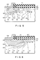
- Figs. 5 and 6 schematically show a flow of the hole current Ih′ on the basis of analysis result obtained by calculation.
- Fig. 5 shows a case wherein a life time is relatively long (to 5 X 10 ⁇ 7 a), and Fig. 6 shows a case wherein a life time is short (to 5 X 10 ⁇ 8 s).
- the distribution of the electrons "e” is localized near the electron storing layer 112 by shortening of the carrier life time, and, as shown in Fig. 6, the holes h are attracted in a direction of the electron storing layer 112.
- the holes h flow in the p-type base region 104 from only near the electron storing layer 112, i.e., only the side surface of the p-type base region 104 and are localized. Therefore, when the carrier life time is sufficiently short, the hole current Ih′ concerning the voltage drop is increased.
- the carrier life time is sufficiently short, the hole current Ih′ concerning the voltage drop is increased.
- the voltage drop is calculated by the following equation: R4 ⁇ Ih4′ + R5 ⁇ Ih5′ ⁇ R5 ⁇ (2/5)Ih
- the present invention has been made in the above consideration, and has as its object to provide a power semiconductor device and, more particularly, an IGBT wherein, when a carrier life time is sufficiently shortened ( ⁇ p ⁇ 1.5 ⁇ 10 ⁇ 7 s ) to realize high-speed turn-OFF characteristics (tf ⁇ 0.3 ⁇ s), a parasitic npn transistor is not easily turned on to obtain a sufficiently large controllable current, and good high-speed turn-OFF characteristics and a sufficiently wide safe operation area can be obtained.
- a power semiconductor device comprising a first region constituted by a semiconductor layer of a first conductivity type; a second region constituted by at least one semiconductor layer of a second conductivity type, formed on said first region, and having an exposed surface; a third region constituted by a semiconductor layer of the first conductivity type which is formed in said second region and a surface of which is exposed to said exposed surface of said second region; a fourth region constituted by a semiconductor layer of the second conductivity type which is formed in said third region and a surface of which is exposed to said exposed surface of said third region; an insulating layer formed on said exposed surfaces of said second, third, and fourth regions; and a gate layer formed on said insulating layer; wherein a carrier life time of the second region is set to be shorter than 5 x 10 ⁇ 7 s by irradiation of a radioactive beam; and said semiconductor device comprises a fifth region formed near said exposed surface on said second region and having an impurity
- a fifth region of a second conductivity type is provided.
- the fifth region is formed in a portion of a second region (drain region) contacting an insulating layer below the gate layer.
- the fifth region contacts a third region (base region) and has an impurity concentration higher than that of the second region.
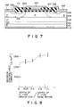
- Fig. 7 is a sectional view showing a power semiconductor device according to the first embodiment of the present invention.
- the same reference numerals in Fig. 7 denote the same parts as in Fig. 1.
- an n-type impurity concentration of a region 1001 located between p-type base regions 104 in an n ⁇ -type drain region 103 is increased.
- a typical impurity concentration of the n-type region 1001 is 1014 to 1017 atm/cc, and the n-type region 1001 is formed to have a uniform impurity concentration distribution in a planar direction.
- the n-type region 1001 is formed to have a depth from the major surface almost equal to the depth of the p-type base region 104 from the major surface.
- an n+-type high-concentration buffer region 102 is epitaxially grown on a p-type silicon substrate (anode) 101 (typical impurity concentration of 1018 to 1020 atm/cc) to have a typical impurity concentration of 1016 to 1017 atm/cc and a thickness of about 10 to 20 ⁇ m, and an n ⁇ -type drain region 103 is epitaxially grown on the buffer region 102 to have a typical impurity concentration of 1013 to 1015 atm/cc and a thickness of about 30 to 100 ⁇ m.
- the n+-type high-concentration buffer region 102 need not be formed and can be omitted depending on a design concept.
- the impurity concentration and thickness of each region are variably selected in accordance with a desired breakdown voltage.
- the impurity concentration and thickness of the n+-type buffer region 102 are respectively set to be 1017 atm/cc and 15 ⁇ m
- the impurity concentration and thickness of the n ⁇ -type drain region 103 are respectively set to be 2 ⁇ 1014 atm/cc and 50 ⁇ m.
- the surface of the drain region 103 of the silicon wafer is oxidized to form an oxide film, and the oxide film is selectively etched using a conventional photoetching method to form an opening leading to an active element forming region of the silicon wafer.
- An n-type impurity is selectively doped into the silicon wafer through the opening.
- phosphorus ions serving as an impurity are implanted in the resultant structure by an ion implantation technique at a dose of 1 ⁇ 1012 ions/cm2. Thereafter, an oxide film is formed over the structure, and the phosphorus ions are diffused in the silicon wafer at a temperature of 1,100°C for several hours to form an n-type region 1001 in the drain region 103.
- the subsequent steps are substantially the same as the steps of manufacturing the conventional IGBT in Fig. 1.
- a p-type region is selectively formed in a guard ring region (not shown in Fig. 7).
- the oxide film on the silicon wafer is removed, and a thin (e.g., about 1,000 ⁇ ) oxide film is formed over the silicon wafer, and a polysilicon layer is epitaxially grown over the thin oxide film to have a thickness of about 5,000 ⁇ .
- the polysilicon layer is patterned to form an internal gate electrode 107.
- a p-type impurity is selectively doped into the region 103 to form the p-type base region 104.
- the thin oxide film is patterned to form a gate oxide film 106 on the active element forming region, and an opening leading to a source forming region.
- An n-type impurity is doped into the source forming region so that an n+-type source region 105 is formed.
- a metal layer made of, for example, aluminum is formed over the surface of the resultant structure and patterned to form a source electrode 108 and a gate electrode 109 on the corresponding regions. Thereafter, an anode electrode 110 is formed on the anode layer 101.
- An electron beam (2 to 10 Mrd) is radiated on the resultant structure to complete a semiconductor device.
- a depth xjp of the p-type base region 104 was set at 4 ⁇ m, and four types of n-type regions 1001 which respectively had depths of 1 ⁇ m (0.25xjp), 2 ⁇ m (0.5xjp), 3.2 ⁇ m (0.8xjp), and 4.4 ⁇ m (1.1xjp) were formed as samples.
- These diffusion depths of the n-type regions 1001 are calculated assuming that a time of impurity diffusion for forming the n-type region 1001 and performed prior to implantation of an impurity for forming the p-type base region 104 corresponds to the diffusion depth.
- concentration distributions of the n-type region 1001 in the direction of depth are 2 ⁇ 1013 atm/cc on the surface, 4.1 ⁇ 1015 atm/cc a depth of 0.5 ⁇ m, 3.8 ⁇ 1015 atm/cc at a depth of 1 ⁇ m, 2.3 ⁇ 1015 atm/cc at a depth of 2 ⁇ m, 9.2 ⁇ 1014 at at a depth of 3 ⁇ m, 3.0 ⁇ 1014 atm/cc at a depth of 4 ⁇ m, and 2 ⁇ 1014 m/cc which is equal to the concentration of a bulk (n ⁇ -type drain region 103) at a depth of 4.4 ⁇ m.
- the n-type region 1001 is deeper than the n+-type source region 105 and has a peak concentration at a depth of 1/8 of the depth xjp of the p-type base region 104, and a profile having a concentration higher than the impurity concentration of the n ⁇ -type drain region 103 by about 10 times at a depth corresponding to 1/8 to 6/8 of the depth xjp is formed.
- FIG. 8 shows the resultant values.
- a point "0" along the abscissa [n-type region depth/p-type base region depth] in Fig. 8 represents the maximum controllable current of an IGBT having the conventional structure (Fig. 1) having no n-type region 1001.
- M the [n-type region depth/p-type base region]
- the maximum controllable current was increased compared with the conventional device in Fig. 1 by about 10%.
- the M was 0.8 or more
- the maximum controllable current was increased by about 20% or more.
- the maximum controllable current was increased by, 26%.
- Fig. 9 is a graph showing variations in maximum controllable current when a carrier life time is changed and when the M is set to be 1.1.
- a carrier life time tp was 5 ⁇ 10 ⁇ 7 s or more (a turn-OFF fall time tf of about 1.0 ⁇ s)
- the maximum controllable current was not largely increased compared with a prior art.
- the carrier life time ⁇ p was 5 ⁇ 10 ⁇ 7 s or less, the maximum controllable current was largely increased.
- Fig. 10 is a sectional view showing the structure of an IGBT according to the above embodiment of the present invention and a flow of npn transistor. That is, in the arrangement of the present invention, since electrons "e" in the n-type region 1001 have a higher distribution density, when the carrier life time is sufficiently shortened, the distribution density of the electrons "e” is high under the p-type base region 104. Therefore, the localization of the hole current Ih′ in the conventional case shown in Fig. 6 is moderated, thereby increasing a maximum controllable current.
- This moderation of localization can be proved by evaluating a relationship between the depth of the n-type region 1001 and the maximum controllable current. When the depth of the n-type region 1001 is increased, the maximum current is increased accordingly. When the depth of the n-type region 1001 is almost equal to that of the p-type base region 104, the maximum controllable current can be optimized. Judging from these evaluation results, the n-type region 1001 contributes to this moderation.
- n-type region 1001 When the n-type region 1001 is formed to have a larger depth, a further increase in maximum controllable current can be expected.
- Fig. 11 is a sectional view showing an IGBT a hole current when the carrier life time ⁇ p is 50 ns.
- a difference between the flow of the hole current in the conventional case shown in Fig. 6 and the flow of the hole current shown in Fig. 10 occurs.
- the difference occurs in the localization of a hole current Ih′ which induces the turn-ON operation of the parasitic according to the second embodiment.
- a deep p+-type base region (body region) 1104 integrated with a p-type base region 104 is formed.
- a carrier life time can be sufficiently shortened to increase a maximum controllable current, as matter of course.
- the present invention has been described on the basis of a basic unit cell sectional structure of an IGBT.
- a large number of basic unit cells are repeatedly arranged.
- a sustaining voltage (avalanche break-down voltage) is decreased.
- a planar geometrical shape of the basic unit cell is important.
- Parameters for determining a sustaining voltage are a strength of an electric field in a depletion region extending from a junction between a p-type base region 104 and an n ⁇ -type drain region 103 (including the n-type region 1001) to the n ⁇ -type drain region 103 (including the n-type region 1001), a corner concentration of the n ⁇ -type drain region 103, and a hole current density, and the sustaining voltage is determined by an avalanche breakdown given by these parameters.
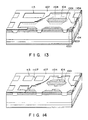
- island-like p-type base regions 104 are respectively formed in a plurality of openings 113 formed in a polysilicon layer which is patterned in a mesh-like form.
- a polysilicon layer 107 is formed in a mesh-like form as in Fig. 12.
- the p-type base region 104 (including a body region 1104) is formed in a ring-like form, and the n-type region 1001 is formed inside the p-type base region 104. Therefore, the n-type region 1001 is an island-like region surrounded by the p-type base region 104 (including the body region 1104).
- the n-type region 1001 is an extended octagon.
- the n-type region 1001 may be a regular octagon and extremely extended. In the latter case, the n-type region 1001 has a so-called stripe-like polysilicon gate structure.
- the semiconductor device of the present invention is desirably embodied combined with the above stripe-like polysilicon gate structure.
- Fig. 14 shows a modification of the device shown in Fig. 7 wherein the device is combined with a stripe-like polysilicon gate structure.
- a polysilicon bridge portion 1107 which crosses a stripe of the p-type base region 104 (including a body region 1104) is formed.
- the pattern of the polysilicon gate has a so-called mesh-like shape. Nevertheless, as the shape of a unit cell, a stripe shape which effectively increases a maximum controllable current is maintained. Since the pattern of the polysilicon gate is close to a mesh-like shape, an internal resistance of the polysilicon gate is reduced compared with the stripe shape. A time constant of the gate circuit is reduced to obtain a power semiconductor device suitable for a high-frequency application.
- the structures shown in Figs. 13 and 14 provide a technique for effectively improving sustaining voltage characteristics and a technique for effectively improving high-speed switching characteristics, respectively.
- Fig. 15 shows a modification of the embodiment shown in Fig. 11, and no n-type region 1001 is formed in a region corresponding to the intersection 114 of the lattice-like n-type region 1001 shown in Fig. 11. That is, the n-type region 1001 having a high impurity concentration is not formed in the region having a high electric field strength. Therefore, when the low impurity concentration is kept, a decrease in avalanche breakdown value, i.e., a decrease in sustaining voltage can be prevented.
- Fig. 16 shows a modification of the application shown in Fig. 13.
- An n-type stripe region 1001 is formed not to contact a p-type base region 104 and also a p+-type body region 1104 at an end of the n-type stripe region 1001 in the longitudinal direction. This has an effect for keeping a low impurity concentration at a relatively high electric field strength at the end of the n-type stripe region 1001 in the longitudinal direction.
- Fig. 17 shows a modification of a termination structure of the devices according to the embodiments of the present invention in Figs. 7 to 11.
- the n-type region 1001 is formed in an entire active region.
- the n-type regions 1001 are formed on not only a portion indicated by diagonal lines descending in the lower right direction but a region 1002.
- the n-type region 1001 is not formed in the region 1002. That is, the n-type region 1001 is not formed in an outermost unit cell of the active region.
- the n-type region 1001 is not formed in a unit cell adjacent to a guard ring region 115 in which a unit cell is not arranged, i.e., to a nonactive region such as a region under a gate electrode metal wire.
- hole current Ih′ flowing into the outermost unit cell in a sustaining mode contains not only a hole current from the active region, but also a hole current from the nonactive region.
- the hole current density of this unit cell is higher than that of general unit cells, and an avalanche breakdown voltage is lower than other unit cells. Therefore, since the n-type region 1001 is not formed, an n-type impurity concentration (doner concentration) can be kept to be low, thereby preventing the reduction of the avalanche breakdown.
- Fig. 18 shows a modification for improving the above problem.
- the n-type region 1001 is not, formed in the outermost unit cell, i.e., in the region 1002, and the n+-type source region 105 is not also formed. For this reason, in the outermost unit cell, a parasitic npn transistor is not constituted. Although the n-type region 1001 is not formed in the region 1002, the unit does not limit the maximum controllable current.
- Embodiments, applications, and modifications of the present invention have been described using n-channel IGBTs as examples. Only when a conductivity type of each region is reversed, the present invention can be applied to a p-channel IGBT as in the n-channel IGBT.
- a power semiconductor device especially an IGBT
- tf ⁇ 0.3 ⁇ s high-speed turn-OFF characteristics
- a carrier life time can be sufficiently shortened ( ⁇ p ⁇ 1.5 ⁇ 1017 s )
- a parasitic npn transistor is not easily turned on, and a sufficiently large controllable current can be obtained. Therefore, a power semiconductor device having good high-speed turn-OFF characteristics and a sufficiently wide safety operation area can be provided.
Landscapes
- Engineering & Computer Science (AREA)
- Microelectronics & Electronic Packaging (AREA)
- Power Engineering (AREA)
- Physics & Mathematics (AREA)
- Ceramic Engineering (AREA)
- Condensed Matter Physics & Semiconductors (AREA)
- General Physics & Mathematics (AREA)
- Computer Hardware Design (AREA)
- Thyristors (AREA)
- Bipolar Transistors (AREA)
- Insulated Gate Type Field-Effect Transistor (AREA)
Applications Claiming Priority (2)
| Application Number | Priority Date | Filing Date | Title |
|---|---|---|---|
| JP234955/89 | 1989-09-11 | ||
| JP1234955A JP2752184B2 (ja) | 1989-09-11 | 1989-09-11 | 電力用半導体装置 |
Publications (2)
| Publication Number | Publication Date |
|---|---|
| EP0417738A1 true EP0417738A1 (fr) | 1991-03-20 |
| EP0417738B1 EP0417738B1 (fr) | 1998-07-22 |
Family
ID=16978878
Family Applications (1)
| Application Number | Title | Priority Date | Filing Date |
|---|---|---|---|
| EP90117501A Expired - Lifetime EP0417738B1 (fr) | 1989-09-11 | 1990-09-11 | Dispositif semi-conducteur de puissance |
Country Status (5)
| Country | Link |
|---|---|
| US (1) | US5124772A (fr) |
| EP (1) | EP0417738B1 (fr) |
| JP (1) | JP2752184B2 (fr) |
| KR (1) | KR940008261B1 (fr) |
| DE (1) | DE69032496T2 (fr) |
Cited By (5)
| Publication number | Priority date | Publication date | Assignee | Title |
|---|---|---|---|---|
| US5326993A (en) * | 1991-04-23 | 1994-07-05 | Fuji Electric Co., Ltd. | Insulated gate bipolar transistor |
| EP0615292A1 (fr) * | 1993-03-10 | 1994-09-14 | Hitachi, Ltd. | Transistor bipolaire à grille isolée |
| US5426314A (en) * | 1992-07-29 | 1995-06-20 | Zaidan Hojin Handotai Kenkyu Shinkokai | Insulated gate control static induction thyristor |
| FR2745952A1 (fr) * | 1996-02-12 | 1997-09-12 | Int Rectifier Corp | Transistor bipolaire a grille isolee a canal court ayant des proprietes ameliorees pour sa chute de tension en sens direct et ses pertes de puissance par commutation |
| DE10009347A1 (de) * | 2000-02-28 | 2001-09-13 | Infineon Technologies Ag | Halbleiterbauelement und entsprechendes Herstellungsverfahren |
Families Citing this family (22)
| Publication number | Priority date | Publication date | Assignee | Title |
|---|---|---|---|---|
| US5528058A (en) * | 1986-03-21 | 1996-06-18 | Advanced Power Technology, Inc. | IGBT device with platinum lifetime control and reduced gaw |
| US5357120A (en) * | 1992-07-14 | 1994-10-18 | Hitachi Ltd. | Compound semiconductor device and electric power converting apparatus using such device |
| JPH06112494A (ja) * | 1992-09-29 | 1994-04-22 | Fuji Electric Co Ltd | 絶縁ゲート型バイポーラトランジスタ |
| US5466951A (en) * | 1993-12-08 | 1995-11-14 | Siemens Aktiengesellschaft | Controllable power semiconductor element with buffer zone and method for the manufacture thereof |
| JP3209091B2 (ja) * | 1996-05-30 | 2001-09-17 | 富士電機株式会社 | 絶縁ゲートバイポーラトランジスタを備えた半導体装置 |
| JP2001501383A (ja) * | 1997-07-30 | 2001-01-30 | シーメンス アクチエンゲゼルシヤフト | ゲート制御されるサイリスタ |
| EP0913872A1 (fr) * | 1997-10-29 | 1999-05-06 | Motorola Semiconducteurs S.A. | Transistor bipolaire à grille isolée |
| JP4164962B2 (ja) * | 1999-10-08 | 2008-10-15 | 株式会社デンソー | 絶縁ゲート型バイポーラトランジスタ |
| JP3490959B2 (ja) * | 2000-07-11 | 2004-01-26 | 三洋電機株式会社 | 受光素子及び受光モジュール |
| JP2002203965A (ja) * | 2000-12-27 | 2002-07-19 | Toshiba Corp | 半導体装置 |
| JP2003069019A (ja) * | 2001-08-29 | 2003-03-07 | Toshiba Corp | 半導体装置およびその製造方法 |
| US6888177B1 (en) * | 2002-09-24 | 2005-05-03 | T-Ram, Inc. | Increased base-emitter capacitance |
| JP2006173437A (ja) * | 2004-12-17 | 2006-06-29 | Toshiba Corp | 半導体装置 |
| JP5036234B2 (ja) | 2006-07-07 | 2012-09-26 | 三菱電機株式会社 | 半導体装置 |
| US20080157117A1 (en) * | 2006-12-28 | 2008-07-03 | Mcnutt Ty R | Insulated gate bipolar transistor with enhanced conductivity modulation |
| US8835987B2 (en) * | 2007-02-27 | 2014-09-16 | Cree, Inc. | Insulated gate bipolar transistors including current suppressing layers |
| JP5435189B2 (ja) * | 2007-10-18 | 2014-03-05 | 文彦 廣瀬 | 電子スイッチ |
| US8629509B2 (en) * | 2009-06-02 | 2014-01-14 | Cree, Inc. | High voltage insulated gate bipolar transistors with minority carrier diverter |
| US8482029B2 (en) * | 2011-05-27 | 2013-07-09 | Infineon Technologies Austria Ag | Semiconductor device and integrated circuit including the semiconductor device |
| US9911838B2 (en) | 2012-10-26 | 2018-03-06 | Ixys Corporation | IGBT die structure with auxiliary P well terminal |
| US9343459B2 (en) * | 2014-04-04 | 2016-05-17 | Texas Instruments Incorporated | Method for creating the high voltage complementary BJT with lateral collector on bulk substrate with resurf effect |
| JP6453120B2 (ja) * | 2015-03-18 | 2019-01-16 | 株式会社日立製作所 | 変圧器 |
Citations (2)
| Publication number | Priority date | Publication date | Assignee | Title |
|---|---|---|---|---|
| GB2088631A (en) * | 1980-12-02 | 1982-06-09 | Gen Electric | Field effect controlled semiconductor rectifier |
| WO1982002981A1 (fr) * | 1981-02-23 | 1982-09-02 | Inc Motorola | Transistor de puissance mos |
Family Cites Families (10)
| Publication number | Priority date | Publication date | Assignee | Title |
|---|---|---|---|---|
| JPS5868979A (ja) * | 1981-10-21 | 1983-04-25 | Hitachi Ltd | 半導体装置 |
| JPS59149058A (ja) * | 1983-02-15 | 1984-08-25 | Matsushita Electric Works Ltd | Mos型トランジスタ |
| JP2585505B2 (ja) * | 1984-09-29 | 1997-02-26 | 株式会社東芝 | 導電変調型mosfet |
| JPS6164165A (ja) * | 1984-09-05 | 1986-04-02 | Matsushita Electric Ind Co Ltd | Mos型電界効果トランジスタ |
| EP0222326A2 (fr) * | 1985-11-12 | 1987-05-20 | General Electric Company | Méthode de fabrication d'un dispositif semi-conducteur ayant une grille isolée |
| JPS62232167A (ja) * | 1986-04-02 | 1987-10-12 | Nissan Motor Co Ltd | 半導体装置 |
| JPS63127571A (ja) * | 1986-11-17 | 1988-05-31 | Nissan Motor Co Ltd | 電導度変調形mosfet |
| JPS6449273A (en) * | 1987-08-19 | 1989-02-23 | Mitsubishi Electric Corp | Semiconductor device and its manufacture |
| US5017508A (en) * | 1989-06-29 | 1991-05-21 | Ixys Corporation | Method of annealing fully-fabricated, radiation damaged semiconductor devices |
| US4925812A (en) * | 1989-09-21 | 1990-05-15 | International Rectifier Corporation | Platinum diffusion process |
-
1989
- 1989-09-11 JP JP1234955A patent/JP2752184B2/ja not_active Expired - Lifetime
-
1990
- 1990-09-10 US US07/579,660 patent/US5124772A/en not_active Expired - Lifetime
- 1990-09-11 KR KR1019900014300A patent/KR940008261B1/ko not_active IP Right Cessation
- 1990-09-11 DE DE69032496T patent/DE69032496T2/de not_active Expired - Lifetime
- 1990-09-11 EP EP90117501A patent/EP0417738B1/fr not_active Expired - Lifetime
Patent Citations (2)
| Publication number | Priority date | Publication date | Assignee | Title |
|---|---|---|---|---|
| GB2088631A (en) * | 1980-12-02 | 1982-06-09 | Gen Electric | Field effect controlled semiconductor rectifier |
| WO1982002981A1 (fr) * | 1981-02-23 | 1982-09-02 | Inc Motorola | Transistor de puissance mos |
Non-Patent Citations (4)
| Title |
|---|
| IEEE TRANSACTIONS ON ELECTRON DEVICES, vol. ED-31, no. 12, December 1984, pages 1790-1795, IEEE, New York, US; B.J. BALIGA: "Switching speed enhancement in insulated gate transistors by electron irradiation" * |
| INTERNATIONAL ELECTRON DEVICES MEETING, Washington, DC, 5th - 7th December 1983, pages 79-82, IEEE, New York, US; A.M. GOODMAN et al.: "Improved COMFETs with fast switching speed and high-current capability" * |
| PATENT ABSTRACTS OF JAPAN, vol. 12, no. 379 (E-667)[3226], 11th October 1988; & JP-A-63 127 571 (NISSAN MOTOR CO., LTD) 31-05-1988 * |
| PATENT ABSTRACTS OF JAPAN, vol. 8, no. 281 (E-286)[1718], 21st December 1984; & JP-A-59 149 058 (MATSUSHIA DENKO K.K.) 25-08-1984 * |
Cited By (8)
| Publication number | Priority date | Publication date | Assignee | Title |
|---|---|---|---|---|
| US5326993A (en) * | 1991-04-23 | 1994-07-05 | Fuji Electric Co., Ltd. | Insulated gate bipolar transistor |
| GB2255228B (en) * | 1991-04-23 | 1995-08-30 | Fuji Electric Co Ltd | Insulated gate bipolar transistor |
| US5426314A (en) * | 1992-07-29 | 1995-06-20 | Zaidan Hojin Handotai Kenkyu Shinkokai | Insulated gate control static induction thyristor |
| EP0615292A1 (fr) * | 1993-03-10 | 1994-09-14 | Hitachi, Ltd. | Transistor bipolaire à grille isolée |
| FR2745952A1 (fr) * | 1996-02-12 | 1997-09-12 | Int Rectifier Corp | Transistor bipolaire a grille isolee a canal court ayant des proprietes ameliorees pour sa chute de tension en sens direct et ses pertes de puissance par commutation |
| US6008092A (en) * | 1996-02-12 | 1999-12-28 | International Rectifier Corporation | Short channel IGBT with improved forward voltage drop and improved switching power loss |
| DE10009347A1 (de) * | 2000-02-28 | 2001-09-13 | Infineon Technologies Ag | Halbleiterbauelement und entsprechendes Herstellungsverfahren |
| DE10009347C2 (de) * | 2000-02-28 | 2003-11-13 | Infineon Technologies Ag | Verfahren zur Herstellung eines Halbleiterbauelements |
Also Published As
| Publication number | Publication date |
|---|---|
| DE69032496T2 (de) | 1999-01-07 |
| US5124772A (en) | 1992-06-23 |
| JPH0397268A (ja) | 1991-04-23 |
| KR910007160A (ko) | 1991-04-30 |
| JP2752184B2 (ja) | 1998-05-18 |
| EP0417738B1 (fr) | 1998-07-22 |
| DE69032496D1 (de) | 1998-08-27 |
| KR940008261B1 (ko) | 1994-09-09 |
Similar Documents
| Publication | Publication Date | Title |
|---|---|---|
| US5124772A (en) | Insulated gate bipolar transistor with a shortened carrier lifetime region | |
| US5268586A (en) | Vertical power MOS device with increased ruggedness and method of fabrication | |
| US7233031B2 (en) | Vertical power semiconductor component | |
| US6975013B2 (en) | Diode and method for manufacturing the same | |
| EP0368246B1 (fr) | Dispositif semi-conducteur bipolaire à grille isolée, ce dispositif comprenant une couche de barrière du type Schottky, et méthode de fabrication correspondante | |
| KR100927505B1 (ko) | n-채널 DMOS 트랜지스터 소스 구조체 및 측방 DMOS 트랜지스터의 제조 방법 | |
| KR100218873B1 (ko) | 절연 게이트형 반도체 장치 및 그 제조방법 | |
| US5701023A (en) | Insulated gate semiconductor device typically having subsurface-peaked portion of body region for improved ruggedness | |
| JP3182262B2 (ja) | 半導体装置 | |
| US20210028279A1 (en) | Cell layouts for mos-gated devices for improved forward voltage | |
| US6147381A (en) | Field effect-controllable semiconductor component | |
| KR20010051995A (ko) | 전력 소자의 단락 회로 내구력을 개선하기 위한 강화된바디 효과가 있는 에미터 안정 저항기 | |
| CN112397593B (zh) | 半导体器件及制造方法 | |
| EP0270975B1 (fr) | Dispositif semi-conducteur de commutation comportant une structure de court-circuit d'anode | |
| KR20010075296A (ko) | 전계 형성 영역을 포함한 반도체 소자 | |
| US20210043734A1 (en) | Semiconductor device and method for producing same | |
| JPH09237904A (ja) | 半導体装置及びその製造方法 | |
| EP0801817B1 (fr) | Dispositifs a semi-conducteurs a grille isolee avec implants conferant plus de robustesse | |
| JPH0685242A (ja) | 半導体装置 |
Legal Events
| Date | Code | Title | Description |
|---|---|---|---|
| PUAI | Public reference made under article 153(3) epc to a published international application that has entered the european phase |
Free format text: ORIGINAL CODE: 0009012 |
|
| 17P | Request for examination filed |
Effective date: 19900911 |
|
| AK | Designated contracting states |
Kind code of ref document: A1 Designated state(s): DE FR GB |
|
| 17Q | First examination report despatched |
Effective date: 19930906 |
|
| GRAG | Despatch of communication of intention to grant |
Free format text: ORIGINAL CODE: EPIDOS AGRA |
|
| GRAG | Despatch of communication of intention to grant |
Free format text: ORIGINAL CODE: EPIDOS AGRA |
|
| GRAH | Despatch of communication of intention to grant a patent |
Free format text: ORIGINAL CODE: EPIDOS IGRA |
|
| GRAH | Despatch of communication of intention to grant a patent |
Free format text: ORIGINAL CODE: EPIDOS IGRA |
|
| GRAA | (expected) grant |
Free format text: ORIGINAL CODE: 0009210 |
|
| AK | Designated contracting states |
Kind code of ref document: B1 Designated state(s): DE FR GB |
|
| REF | Corresponds to: |
Ref document number: 69032496 Country of ref document: DE Date of ref document: 19980827 |
|
| ET | Fr: translation filed | ||
| PLBE | No opposition filed within time limit |
Free format text: ORIGINAL CODE: 0009261 |
|
| STAA | Information on the status of an ep patent application or granted ep patent |
Free format text: STATUS: NO OPPOSITION FILED WITHIN TIME LIMIT |
|
| 26N | No opposition filed | ||
| REG | Reference to a national code |
Ref country code: GB Ref legal event code: IF02 |
|
| PGFP | Annual fee paid to national office [announced via postgrant information from national office to epo] |
Ref country code: GB Payment date: 20090909 Year of fee payment: 20 |
|
| PGFP | Annual fee paid to national office [announced via postgrant information from national office to epo] |
Ref country code: DE Payment date: 20090903 Year of fee payment: 20 |
|
| PGFP | Annual fee paid to national office [announced via postgrant information from national office to epo] |
Ref country code: FR Payment date: 20091012 Year of fee payment: 20 |
|
| REG | Reference to a national code |
Ref country code: GB Ref legal event code: PE20 Expiry date: 20100910 |
|
| PG25 | Lapsed in a contracting state [announced via postgrant information from national office to epo] |
Ref country code: GB Free format text: LAPSE BECAUSE OF EXPIRATION OF PROTECTION Effective date: 20100910 |
|
| PG25 | Lapsed in a contracting state [announced via postgrant information from national office to epo] |
Ref country code: DE Free format text: LAPSE BECAUSE OF EXPIRATION OF PROTECTION Effective date: 20100911 |