EP0346035A2 - Anschlussstruktur und Verfahren zu deren Herstellung - Google Patents
Anschlussstruktur und Verfahren zu deren Herstellung Download PDFInfo
- Publication number
- EP0346035A2 EP0346035A2 EP89305629A EP89305629A EP0346035A2 EP 0346035 A2 EP0346035 A2 EP 0346035A2 EP 89305629 A EP89305629 A EP 89305629A EP 89305629 A EP89305629 A EP 89305629A EP 0346035 A2 EP0346035 A2 EP 0346035A2
- Authority
- EP
- European Patent Office
- Prior art keywords
- group
- teeth
- stem
- substrate
- extending
- Prior art date
- Legal status (The legal status is an assumption and is not a legal conclusion. Google has not performed a legal analysis and makes no representation as to the accuracy of the status listed.)
- Granted
Links
Images


Classifications
-
- H—ELECTRICITY
- H01—ELECTRIC ELEMENTS
- H01R—ELECTRICALLY-CONDUCTIVE CONNECTIONS; STRUCTURAL ASSOCIATIONS OF A PLURALITY OF MUTUALLY-INSULATED ELECTRICAL CONNECTING ELEMENTS; COUPLING DEVICES; CURRENT COLLECTORS
- H01R12/00—Structural associations of a plurality of mutually-insulated electrical connecting elements, specially adapted for printed circuits, e.g. printed circuit boards [PCB], flat or ribbon cables, or like generally planar structures, e.g. terminal strips, terminal blocks; Coupling devices specially adapted for printed circuits, flat or ribbon cables, or like generally planar structures; Terminals specially adapted for contact with, or insertion into, printed circuits, flat or ribbon cables, or like generally planar structures
- H01R12/50—Fixed connections
- H01R12/51—Fixed connections for rigid printed circuits or like structures
- H01R12/55—Fixed connections for rigid printed circuits or like structures characterised by the terminals
- H01R12/57—Fixed connections for rigid printed circuits or like structures characterised by the terminals surface mounting terminals
-
- H—ELECTRICITY
- H05—ELECTRIC TECHNIQUES NOT OTHERWISE PROVIDED FOR
- H05K—PRINTED CIRCUITS; CASINGS OR CONSTRUCTIONAL DETAILS OF ELECTRIC APPARATUS; MANUFACTURE OF ASSEMBLAGES OF ELECTRICAL COMPONENTS
- H05K3/00—Apparatus or processes for manufacturing printed circuits
- H05K3/30—Assembling printed circuits with electric components, e.g. with resistors
- H05K3/32—Assembling printed circuits with electric components, e.g. with resistors electrically connecting electric components or wires to printed circuits
- H05K3/34—Assembling printed circuits with electric components, e.g. with resistors electrically connecting electric components or wires to printed circuits by soldering
- H05K3/3405—Edge mounted components, e.g. terminals
-
- H—ELECTRICITY
- H10—SEMICONDUCTOR DEVICES; ELECTRIC SOLID-STATE DEVICES NOT OTHERWISE PROVIDED FOR
- H10W—GENERIC PACKAGES, INTERCONNECTIONS, CONNECTORS OR OTHER CONSTRUCTIONAL DETAILS OF DEVICES COVERED BY CLASS H10
- H10W70/00—Package substrates; Interposers; Redistribution layers [RDL]
- H10W70/01—Manufacture or treatment
- H10W70/05—Manufacture or treatment of insulating or insulated package substrates, or of interposers, or of redistribution layers
- H10W70/093—Connecting or disconnecting other interconnections thereto or therefrom, e.g. connecting bond wires or bumps
-
- H—ELECTRICITY
- H10—SEMICONDUCTOR DEVICES; ELECTRIC SOLID-STATE DEVICES NOT OTHERWISE PROVIDED FOR
- H10W—GENERIC PACKAGES, INTERCONNECTIONS, CONNECTORS OR OTHER CONSTRUCTIONAL DETAILS OF DEVICES COVERED BY CLASS H10
- H10W70/00—Package substrates; Interposers; Redistribution layers [RDL]
- H10W70/60—Insulating or insulated package substrates; Interposers; Redistribution layers
- H10W70/67—Insulating or insulated package substrates; Interposers; Redistribution layers characterised by their insulating layers or insulating parts
- H10W70/69—Insulating materials thereof
-
- H—ELECTRICITY
- H10—SEMICONDUCTOR DEVICES; ELECTRIC SOLID-STATE DEVICES NOT OTHERWISE PROVIDED FOR
- H10W—GENERIC PACKAGES, INTERCONNECTIONS, CONNECTORS OR OTHER CONSTRUCTIONAL DETAILS OF DEVICES COVERED BY CLASS H10
- H10W90/00—Package configurations
- H10W90/701—Package configurations characterised by the relative positions of pads or connectors relative to package parts
-
- H—ELECTRICITY
- H05—ELECTRIC TECHNIQUES NOT OTHERWISE PROVIDED FOR
- H05K—PRINTED CIRCUITS; CASINGS OR CONSTRUCTIONAL DETAILS OF ELECTRIC APPARATUS; MANUFACTURE OF ASSEMBLAGES OF ELECTRICAL COMPONENTS
- H05K2201/00—Indexing scheme relating to printed circuits covered by H05K1/00
- H05K2201/09—Shape and layout
- H05K2201/09209—Shape and layout details of conductors
- H05K2201/09654—Shape and layout details of conductors covering at least two types of conductors provided for in H05K2201/09218 - H05K2201/095
- H05K2201/09709—Staggered pads, lands or terminals; Parallel conductors in different planes
-
- H—ELECTRICITY
- H05—ELECTRIC TECHNIQUES NOT OTHERWISE PROVIDED FOR
- H05K—PRINTED CIRCUITS; CASINGS OR CONSTRUCTIONAL DETAILS OF ELECTRIC APPARATUS; MANUFACTURE OF ASSEMBLAGES OF ELECTRICAL COMPONENTS
- H05K2201/00—Indexing scheme relating to printed circuits covered by H05K1/00
- H05K2201/10—Details of components or other objects attached to or integrated in a printed circuit board
- H05K2201/10227—Other objects, e.g. metallic pieces
- H05K2201/1034—Edge terminals, i.e. separate pieces of metal attached to the edge of the printed circuit board [PCB]
-
- H—ELECTRICITY
- H05—ELECTRIC TECHNIQUES NOT OTHERWISE PROVIDED FOR
- H05K—PRINTED CIRCUITS; CASINGS OR CONSTRUCTIONAL DETAILS OF ELECTRIC APPARATUS; MANUFACTURE OF ASSEMBLAGES OF ELECTRICAL COMPONENTS
- H05K2201/00—Indexing scheme relating to printed circuits covered by H05K1/00
- H05K2201/10—Details of components or other objects attached to or integrated in a printed circuit board
- H05K2201/10613—Details of electrical connections of non-printed components, e.g. special leads
- H05K2201/10954—Other details of electrical connections
- H05K2201/10977—Encapsulated connections
-
- H—ELECTRICITY
- H05—ELECTRIC TECHNIQUES NOT OTHERWISE PROVIDED FOR
- H05K—PRINTED CIRCUITS; CASINGS OR CONSTRUCTIONAL DETAILS OF ELECTRIC APPARATUS; MANUFACTURE OF ASSEMBLAGES OF ELECTRICAL COMPONENTS
- H05K3/00—Apparatus or processes for manufacturing printed circuits
- H05K3/30—Assembling printed circuits with electric components, e.g. with resistors
- H05K3/32—Assembling printed circuits with electric components, e.g. with resistors electrically connecting electric components or wires to printed circuits
- H05K3/34—Assembling printed circuits with electric components, e.g. with resistors electrically connecting electric components or wires to printed circuits by soldering
- H05K3/341—Surface mounted components
- H05K3/3421—Leaded components
-
- Y—GENERAL TAGGING OF NEW TECHNOLOGICAL DEVELOPMENTS; GENERAL TAGGING OF CROSS-SECTIONAL TECHNOLOGIES SPANNING OVER SEVERAL SECTIONS OF THE IPC; TECHNICAL SUBJECTS COVERED BY FORMER USPC CROSS-REFERENCE ART COLLECTIONS [XRACs] AND DIGESTS
- Y10—TECHNICAL SUBJECTS COVERED BY FORMER USPC
- Y10T—TECHNICAL SUBJECTS COVERED BY FORMER US CLASSIFICATION
- Y10T29/00—Metal working
- Y10T29/49—Method of mechanical manufacture
- Y10T29/49002—Electrical device making
- Y10T29/49117—Conductor or circuit manufacturing
- Y10T29/49121—Beam lead frame or beam lead device
-
- Y—GENERAL TAGGING OF NEW TECHNOLOGICAL DEVELOPMENTS; GENERAL TAGGING OF CROSS-SECTIONAL TECHNOLOGIES SPANNING OVER SEVERAL SECTIONS OF THE IPC; TECHNICAL SUBJECTS COVERED BY FORMER USPC CROSS-REFERENCE ART COLLECTIONS [XRACs] AND DIGESTS
- Y10—TECHNICAL SUBJECTS COVERED BY FORMER USPC
- Y10T—TECHNICAL SUBJECTS COVERED BY FORMER US CLASSIFICATION
- Y10T29/00—Metal working
- Y10T29/49—Method of mechanical manufacture
- Y10T29/49002—Electrical device making
- Y10T29/49117—Conductor or circuit manufacturing
- Y10T29/49124—On flat or curved insulated base, e.g., printed circuit, etc.
- Y10T29/49147—Assembling terminal to base
- Y10T29/49149—Assembling terminal to base by metal fusion bonding
-
- Y—GENERAL TAGGING OF NEW TECHNOLOGICAL DEVELOPMENTS; GENERAL TAGGING OF CROSS-SECTIONAL TECHNOLOGIES SPANNING OVER SEVERAL SECTIONS OF THE IPC; TECHNICAL SUBJECTS COVERED BY FORMER USPC CROSS-REFERENCE ART COLLECTIONS [XRACs] AND DIGESTS
- Y10—TECHNICAL SUBJECTS COVERED BY FORMER USPC
- Y10T—TECHNICAL SUBJECTS COVERED BY FORMER US CLASSIFICATION
- Y10T29/00—Metal working
- Y10T29/49—Method of mechanical manufacture
- Y10T29/49002—Electrical device making
- Y10T29/49117—Conductor or circuit manufacturing
- Y10T29/49174—Assembling terminal to elongated conductor
- Y10T29/49179—Assembling terminal to elongated conductor by metal fusion bonding
Definitions
- the present invention relates to a terminal structure and a process of fabricating it.
- it relates to a process of fabricating a hybrid-IC device having a multiplicity of input and output terminals, and a terminal structure thereof.
- it relates to a mounting structure for input and output terminals of modules such as IC, LSI, etc., and more particularly to a mounting structure for a one-surface terminals.
- a prior-art hybrid IC device of the type having a multiplicity of input and output terminals is soldered to a substrate by reflow of the components and the input and output terminals are also soldered onto the substrate.
- one end of each lead 71 is bent to have an inverted U-shape 73, and the tip 72 of the lead 71 is made to abut a soldering pad 75 substantially at right angles to permit soldering by reflow (Japanese Utility Model Application Kokai Publication No. 43,452/1988).
- a lead frame 81 is formed substantially in a hat shape, a notch 84 is provided in part of the hat to clamp the substrate, and soldering is performed by dipping, and the connecting part 83 is later removed to form lead terminals (Japanese Patent Application Kokai Publication No. 266,856/1987).
- the throughhole pitch of the mother board on which a hybrid IC device is mounted is standardized and is usually 2.54mm for the reason of strength, easy manipulation, etc.
- To obtain connection of input and output terminals in a limited length of mounting it is necessary to arrange them in a plurality of rows.
- modules such as IC, LSI, etc.
- modules have such a structure shown in Fig. 3 to Fig. 7, and connected to the substrate in the module.
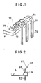
- Fig. 3 shows an example in which clip terminals are used.
- the substrate 101 of the module has a surface on which electronic components, devices, etc., not shown, are mounted, and these components, devices, etc. are electrically connected by means of a wiring pattern, not shown.
- the wiring pattern has terminal pads 102a for connection with the input and output terminals at an end of the substrate 101.
- the clip terminal 109 clamps the substrate 101 by virtue of its resiliency.
- the clip terminal 109 and the substrate 101 are fixed provisionally. In this state, the clip terminal 109 and the terminal pads 102a are electrically connected by solder 103a, so good values are obtained with regard to the reliability of the connection resistance and the pull strength.
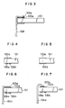
- wiring patterns 106a and 106b are provided as shown in Fig. 4, or additional terminal pads 102b are provided on the reverse surfaces of the substrate 101 as shown in Fig. 5.
- the clip terminals shown in Fig. 3 cannot be used, so one-surface terminals 104c and 104e in abutment with one surface of the substrate 101 are used and fixed to terminal pads 102a with solder 103a.
- the substrate With the structure shown in Fig. 3, the substrate is clamped on both surfaces, so wiring patterns and terminal pads cannot be disposed on the reverse surface of the substrate, and therefore the input and output terminals cannot be provided on both surfaces of the substrate.
- the terminals With the structure shown in Fig. 6 and Fig. 7, the terminals are in contact with only a single surface of the substrate, so there is a problem that the reliability of the connection resistance and the pull strength is low, compared with the clip terminals shown in Fig. 3.
- the one-surface terminal and the substrate are fixed by solder alone, a large quantity of solder is required and the areas for the terminal pads are substantial.
- An object of the present invention is to mount a multiplicity of terminals on both surfaces of a substrate for a hybrid IC device, and fix them by reflow.
- Another object of the present invention is to provide a structure and a method for mounting a terminal having a high pull-strength and connection resistance reliability, reduced terminal pad areas, and thereby to enable a high-density mounting.
- a multiple-terminal unit comprises: a band-shaped connecting part; a first and a second group of teeth extending from one edge of the connecting part; said first group consisting of teeth provided at alternate positions and said second group consisting of teeth provided at intervening positions; each tooth in said first group having a stem part having one end continuous with the connecting part and extending in the same plane as the connecting part, a lateral part having one end continuous with the other end of the stem part, and extending at an angle with the stem part, and an end part having one end continuous with the lateral part and extending in parallel with the stem part; each tooth in said second group having a lateral part having one end continuous with the connecting part and extending at an angle with the connecting part, a stem part having one end continuous with the other end of the lateral part and extending in parallel with the connecting part, and an end part having one end continuous with the stem part and extending in the same plane as the stem part; said end parts of said teeth in said first group and said second group being aligned with each other
- a multiple-terminal unit formed as recited above is provided; a substrate with soldering paste printed in pad regions on the substrate is provided; the end parts of said teeth of said multiple-terminal unit are soldered with the printed soldering paste in the pad regions on the substrate; and the connecting part of the multiple-terminal unit is then removed.
- the stem parts of the resultant terminals fixed to the substrate of the hybrid IC device are staggered, i.e., arranged in a zigzag manner.
- the throughhole pitch of a standardized value, e.g., 2.54mm of the mother board is maintained, and the strength and easy manipulation are not impaired, and the terminals are disposed in a plurality of rows.
- a mounting structure of a one-surface terminal has a contact with one surface only of a substrate for an electronic component module and electrically connected to a wiring pattern on the substrate, wherein the part at which said one-surface terminal and said wiring pattern are connected are fixed by resin, preferably thixotropic resin.
- said one-surface terminal and said wiring pattern are soldered; resin is applied on the part of the connection; and the resin is hardened to fix said substrate and said one-surface terminal.
- the above-mentioned resin is a thixotropic resin.
- Use of thixotropic resin is advantageous in that it can completely cover the part of the connection and has such a viscosity and does not flow out of the part in which it is applied.
- the resin applied to the part of connection of the terminal has a property of a thixotropic fluid.
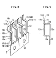
- Fig. 8 is an oblique view showing a multiple-terminal unit of an embodiment of the invention.
- Fig. 9 is a sectional view along line IX-IX in Fig. 8.
- the multiple-terminal unit comprises a substantially band-shaped connecting part 11, and a first group of teeth 12 and a second group of teeth 13 extending from one edge of the band-shaped connecting part 11.
- Each of the teeth 12 in the first group has a first stem part 12a having one end continuous with the connecting part 11 and extending in the same plane as the connecting part 11; a lateral part 12b having one end continuous with the other end of the stem part 12a and extending at an angle, e.g., almost at a right angle, with the stem part 12a, and an end part 12c having one end continuous with the other end of the lateral part 12b and extending in parallel with the stem part 12a.
- Each of the teeth 13 in the second group has a lateral part 13a having one end continuous with the connecting part 11 and extending at an angle, e.g., almost at a right angle, with the connecting part 11, a stem part 13b having one end continuous with the other end of the lateral part 13a and extending in parallel with the connecting part 11, and an end part 13c having one end continuous with the other end of the stem part 13b and extending in the same plane as the stem part 13b.
- the end parts 12c and 13c of the teeth 12 and 13 in the first and second groups are all aligned with respect to each other along a single row, and the extremities 12d and 13d of the end parts 12c and 13c are all aligned with respect to each other.
- the stem parts 12a of the teeth 12 in the first group are aligned with each other and are arranged at a pitch equal to the throughhole pitch of the mother board on which the hybrid IC device is to mounted, and the stem parts 13b of the teeth 13 in the second group 13 are aligned with each other and are arranged at the same pitch as that of the stem parts 12a.
- the stem parts 12a and 13b of the teeth 12 and 13 are shifted in the lateral direction, i.e. the direction of the thickness of the connecting part 11, and are also shifted relative to each other in the direction of the rows of the teeth 12 and 13.
- the distance by which the stem parts 12a and 13b of the teeth 12 and 13 are shifted relative to each other in the lateral direction is the above-mentioned throughhole pitch of the mother board, and the distance by which the stem parts 12a and 13b are shifted relative to each other in the direction of the rows of the teeth 12 and 13 is half that of the above-mentioned throughhole pitch of the mother board.
- the terminal unit 1 shown in Fig. 8 and Fig. 9 can be formed by continuous punching and bending. That is, a metal sheet is punched to form a comb-shaped pattern of metal sheet, as illustrated in Fig. 10. As illustrated in Fig. 10, the comb-shaped pattern has the connecting part 11 and teeth T which will later become the teeth 12 and 13.
- the comb-shaped pattern is then subjected to a bending process to result in the structure as shown in Fig. 8.
- alternate teeth T are bent at about a right angle in a first direction to form a convex bend 14 at a first position B1 relatively far away from the connecting part 11, and also bent at about a right angle to form a concave bend 15 at a second position B2 at a height (position in the vertical direction as seen in Fig. 8 and Fig. 9) close to the height of the convex bend B1.
- the intervening teeth T are bent at about a right angle to form a convex bend 16 at a third position B3 close to the connecting part 11, and also bent at about a right angle at a fourth position B4 to form a concave bend 17 at a height (position in the vertical direction as seen in Fig. 8 and Fig. 9) close to height of the convex bend B3.
- the end parts 12c and 13c form soldering parts, which will be fixed to terminal pads of a substrate 2 shown in Fig. 11D and Fig. 12.
- Fig. 11A to Fig. 11E show how a hybrid IC is formed using the terminal units of the above embodiment.
- Fig. 11A shows a substrate 2 with solder paste 3 having been printed on its reverse surface.
- solder paste 3 is printed only for the terminal pads 21 on the substrate 2.
- solder paste 3 is printed on the component mounting surface (obverse surface) of the substrate 2, for the terminal pads 22, and component pads 23 and 24.
- components 5 and 6 are mounted.
- Fig. 3D a pair of the multiple-terminal units 2 are set or fixed to the substrate 2.
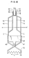
- Fig. 12 shows in greater detail how the multiple-terminal units 1 are fixed onto a substrate 2.
- Two multiple-terminal units 1 are used in combination, and are made to confront each other, and their connecting parts 11 are held between a fixed block 43 and clamping parts 41 and 42 of a clamp jig 4.
- the soldering parts 18 of the multiple-terminal units 1 held by the clamp jig 4 are little widened and, the soldering parts 12 of the multiple-terminal units 1 are made to abut the terminal pads 21 and 22 of the substrate 2.
- the substrate 2 the multiple-terminal units 1 and the clamping jig 4 are held.
- the assembly is then passed through a reflow apparatus, and the components 5 and 6, and the multiple-terminal units 1 are simultaneously soldered.
- the terminal pads 21 and 22 on the substrate 2 and the soldering parts 18 of the terminal units 1 are fixed and connected by solder 3.
- the stem parts 12a and 13b of the teeth 12 and 13 of the terminal units 1 are cut at the same height (vertical position as seen in Fig. 12), and the parts below (as seen in Fig. 12) the cut line X-X′ in Fig. 12 which include the connecting parts 11 and the lower (as seen in Fig. 12) parts of the stem parts 12a and the stem parts 13b, and the lateral parts 13a are removed.
- the resultant structure is shown in Fig. 11E.
- the terminals can be divided into two groups, the first group consisting of terminals 32 at alternate positions and the second group consisting of terminals 33 at intervening positions.
- the terminals 32 of first group are formed from the teeth 12 of the first group.
- the terminals 33 of the second group 33 are formed from the teeth 13 of the second group.
- Each of the terminals 32 in the first group has a soldering part 32c which is formed of the end part 12c of each tooth 12, a lateral part 32b which is formed of the lateral part 12b, and a stem part 32a which is formed of the upper (as seen in Fig. 12) part of the stem part 12a of the tooth 12.
- Each of the terminals 33 in the second group has a soldering part 33c which is formed of the end part 13c of each tooth 13, and a stem part 33b which is formed of the upper (as seen in Fig. 12) part of the stem part 13b of the tooth 13.
- the ends 32e and 33e of the stem parts 32a and 33b form soldering parts, which will be inserted in and soldered to throughholes in the mother board, not shown.
- the stem parts 32a of the terminals 32 in the first group are aligned with each other and are arranged at a pitch equal to the throughhole pitch of the mother board, and the stem parts 33b of the terminals 33 in the second group are aligned with each other and are arranged at the same pitch as that of the stem parts 32a.
- the stem parts 32a and 33b of the terminals 32 and 33 are shifted relative to each other in the lateral direction, and are also shifted relative to each other in the direction of the rows of the terminals 32 and 33.
- the distance by which the stem parts 32a and 33b of the terminals 32 and 33 are are shifted relative to each other in the lateral direction is the above-mentioned throughhole pitch of the mother board, and the distance by which the stem parts 32a and 33b are shifted relative to each other in the direction of the rows of the terminals 32 and 33 is half that of the above-mentioned throughhole pitch of the mother board.
- the extremities 32f and 33f of the terminals 32 and 33 are staggered or arranged in a zigzag manner.
- the input and output terminals of a hybrid IC device are formed, being staggered, and a high-density mounting is therefore possible. Because the terminals adjacent to each other are both bent at a first position and a second position in the same way, the layout size for the continuous punching and bending process can be minimized, and a high-precision is achieved in the dimension of the resultant structure. Moreover, the assembly of the terminals are reflowed simultaneously with the mounted components so that the cost for the multiple-terminal units are lowered. It is therefore possible to provide a multiple-terminal hybrid IC device of a low cost suitable for a high density mounting.
- terminal pads are provided on both surfaces of the substrate.
- terminal pads 102a on one surface thereof and terminal pads 102b on the other surface thereof are terminal pads 102a on one surface thereof and terminal pads 102b on the other surface thereof. These terminal pads 102a and 102b both form part of a wiring pattern, not shown, which is formed on the substrate 101.
- Connected to the terminal pads 102a and 102b are one-surface terminals 104a and 104b by means of solder 103a and 103b.
- the wiring pattern, not shown, on the substrate 101 and the one-surface terminals 104a and 104b are thereby electrically connected.
- Resin 105a, 105b covers the connection parts and fixes the substrate 101 and the one-surface terminals 104a and 104b.
- the resin 105a, 105b must have a sufficient strength to fix the substrate 101 and the one-surface terminals 104a and 104b, and must not flow out of the application area when applied onto the substrate 101.
- Resin having thixotropic property is preferable. In an ordinary state, this resin has a viscosity of 1000 to 1500 poise when measured using B8H-type viscosity meter, under the condition of rotor No. 7, the rotational speed of 20 rpm and the temperature of 25 o C, and in the method defined by JIS-C-2105.
- the resin has a thixotropy index of 1.0 to 1.5.
- the thixotropy index is a value defined by the following equation:
- the viscosity is measured using B8H-type viscosity meter, rotor No. 7 and at temperature 25°C, and in compliance with JIS-K-6838.
- the resin has the above-described viscosity and thixotropy index, the resin can be easily applied to the substrate and does not flow out of the application area after being applied.
- Fig. 15 is a side sectional view showing another embodiment of the invention, in which terminal pads 102a are formed on both ends on one surface of the substrate 101. Electrically connected to the terminal pads 102a by means of solder 103a are one-surface terminals 104c and 104d. Formed on the other surface of the substrate 101 are wiring patterns 106a, 106b and 106c. As is in the embodiment of Fig. 14, the substrate 101 and the one-surface terminals 104c and 104d are fixed by resin 105c, 105d.
- terminal pads 102a and 102b are formed on both surfaces of an end of the substrate 101.
- terminal pads 102a and 102b are formed on both surfaces of an end of the substrate 101.
- solder cream 107a, 107b is printed (Fig. 16A).
- the one-surface terminals 104a and 104b are made to abut the surface of the printed solder cream 107a (Fig. 16B), and soldering and fixing are effected by reflow.
- the soldering pads 102a and 102b, and the one-surface terminals 104a and 104b are thus bonded and electrically connected (Fig. 16C).
- resin 105a, 105b is emitted from a dispenser 108, and applied onto the terminal pads 102a and 102b, and the one-surface terminals 104a and 104b (Fig. 16D).
- the resin 105a, 105b is thixotropic fluid, and its viscosity decreases with time when shearing deformation or shearing velocity is given. Its viscosity restores when it is left without giving the shearing deformation or shearing velocity. That is, the apparent viscosity varies reversibly.
- the viscosity of the resin returns to the original state.
- the resin 105a, 105b adheres to the substrate 101 and does not flow out of the terminal pads 102a and 102b even if the substrate 101 is inclined.
- the resin is therefore kept attached to the part at which the terminal pads 102a and 102b and the one-surface terminals 104a and 104b are connected.
- the resin 105a, 105b is hardened by heating or the like, so that the substrate 101 and the one-surface terminals 104a and 104b are fixed.
Landscapes
- Engineering & Computer Science (AREA)
- Manufacturing & Machinery (AREA)
- Microelectronics & Electronic Packaging (AREA)
- Coupling Device And Connection With Printed Circuit (AREA)
- Structures For Mounting Electric Components On Printed Circuit Boards (AREA)
- Manufacturing Of Electrical Connectors (AREA)
- Electric Connection Of Electric Components To Printed Circuits (AREA)
- Multi-Conductor Connections (AREA)
Applications Claiming Priority (4)
| Application Number | Priority Date | Filing Date | Title |
|---|---|---|---|
| JP63140552A JPH0732041B2 (ja) | 1988-06-09 | 1988-06-09 | 多端子ハイブリッドicの端子取付構造 |
| JP140553/88 | 1988-06-09 | ||
| JP14055388A JPH01310570A (ja) | 1988-06-09 | 1988-06-09 | 片面端子取付構造及びその取付方法 |
| JP140552/88 | 1988-06-09 |
Related Child Applications (2)
| Application Number | Title | Priority Date | Filing Date |
|---|---|---|---|
| EP93202116A Division EP0577223A1 (de) | 1988-06-09 | 1989-06-05 | Anordnung zum Montieren eins Endverbinders |
| EP93202116.5 Division-Into | 1993-07-20 |
Publications (3)
| Publication Number | Publication Date |
|---|---|
| EP0346035A2 true EP0346035A2 (de) | 1989-12-13 |
| EP0346035A3 EP0346035A3 (de) | 1991-01-16 |
| EP0346035B1 EP0346035B1 (de) | 1994-08-31 |
Family
ID=26473032
Family Applications (2)
| Application Number | Title | Priority Date | Filing Date |
|---|---|---|---|
| EP93202116A Ceased EP0577223A1 (de) | 1988-06-09 | 1989-06-05 | Anordnung zum Montieren eins Endverbinders |
| EP89305629A Expired - Lifetime EP0346035B1 (de) | 1988-06-09 | 1989-06-05 | Anschlussstruktur und Verfahren zu deren Herstellung |
Family Applications Before (1)
| Application Number | Title | Priority Date | Filing Date |
|---|---|---|---|
| EP93202116A Ceased EP0577223A1 (de) | 1988-06-09 | 1989-06-05 | Anordnung zum Montieren eins Endverbinders |
Country Status (3)
| Country | Link |
|---|---|
| US (3) | US4985747A (de) |
| EP (2) | EP0577223A1 (de) |
| DE (1) | DE68917798T2 (de) |
Cited By (8)
| Publication number | Priority date | Publication date | Assignee | Title |
|---|---|---|---|---|
| WO1992020100A1 (en) * | 1991-04-30 | 1992-11-12 | International Business Machines Corporation | A ceramic substrate having a protective coating and method of protection |
| EP0516149A1 (de) * | 1991-05-31 | 1992-12-02 | Nippondenso Co., Ltd. | Elektronische Vorrichtung |
| EP0556550A3 (de) * | 1992-02-18 | 1994-04-06 | Ibm | |
| US5586389A (en) * | 1991-05-31 | 1996-12-24 | Nippondenso Co., Ltd. | Method for producing multi-board electronic device |
| US5646827A (en) * | 1991-05-31 | 1997-07-08 | Nippondenso Co., Ltd. | Electronic device having a plurality of circuit boards arranged therein |
| US5657203A (en) * | 1991-05-31 | 1997-08-12 | Nippondenso Co., Ltd. | Electronic device having a plurality of circuit boards arranged therein |
| EP0822737A3 (de) * | 1996-07-31 | 2000-05-10 | Oki Electric Industry Co., Ltd. | Einheits-Anschlussleiste, Verbindungsverfahren, Verbindungsplatine sowie Herstellunsgverfahren |
| CN115486212A (zh) * | 2020-05-12 | 2022-12-16 | 塔克托科技有限公司 | 用于纳入整合式多层结构中的连接结构 |
Families Citing this family (21)
| Publication number | Priority date | Publication date | Assignee | Title |
|---|---|---|---|---|
| US5586388A (en) * | 1991-05-31 | 1996-12-24 | Nippondenso Co., Ltd. | Method for producing multi-board electronic device |
| US5364280A (en) * | 1993-07-16 | 1994-11-15 | Molex Incorporated | Printed circuit board connector assembly |
| JP3114473B2 (ja) * | 1993-12-22 | 2000-12-04 | 松下電器産業株式会社 | コネクタの実装方法 |
| US6339191B1 (en) * | 1994-03-11 | 2002-01-15 | Silicon Bandwidth Inc. | Prefabricated semiconductor chip carrier |
| US5821457A (en) * | 1994-03-11 | 1998-10-13 | The Panda Project | Semiconductor die carrier having a dielectric epoxy between adjacent leads |
| US5824950A (en) * | 1994-03-11 | 1998-10-20 | The Panda Project | Low profile semiconductor die carrier |
| US5490786A (en) * | 1994-03-25 | 1996-02-13 | Itt Corporation | Termination of contact tails to PC board |
| JP2929937B2 (ja) * | 1994-04-20 | 1999-08-03 | 松下電器産業株式会社 | 電子部品実装装置及び電子部品の実装方法 |
| JP2782673B2 (ja) * | 1995-06-23 | 1998-08-06 | 関西日本電気株式会社 | 電界発光灯 |
| EP0793853A1 (de) * | 1995-06-30 | 1997-09-10 | Koninklijke Philips Electronics N.V. | Oberflächenmontierbare elektrische komponenten |
| EP0952761A4 (de) * | 1996-05-31 | 2005-06-22 | Rohm Co Ltd | Verfahren zur montierung eines anschlussleiters auf einer leiterplatte und leiterplatte |
| US6141869A (en) | 1998-10-26 | 2000-11-07 | Silicon Bandwidth, Inc. | Apparatus for and method of manufacturing a semiconductor die carrier |
| US6227867B1 (en) * | 1999-02-03 | 2001-05-08 | Hon Hai Precision Ind. Co., Ltd. | Method for performing double-sided SMT |
| US6647603B2 (en) * | 2001-11-05 | 2003-11-18 | Ceramate Technical Co., Ltd. | Process for manufacturing electronic device packages |
| USD472530S1 (en) | 2001-11-30 | 2003-04-01 | Mitsubishi Denki Kabushiki Kaisha | Semiconductor device |
| USD470824S1 (en) | 2001-11-30 | 2003-02-25 | Mitsubishi Denki Kabushiki Kaisha | Semiconductor device |
| USD470463S1 (en) | 2001-11-30 | 2003-02-18 | Mitsubishi Denki Kabushiki Kaisha | Semiconductor device |
| DE102004013757B4 (de) * | 2004-03-20 | 2007-03-08 | Mc Technology Gmbh | Elektrischer Koppelbaustein |
| US7625496B2 (en) * | 2006-11-03 | 2009-12-01 | Chemtura Corporation | Solid composition for treating water |
| US7566963B2 (en) * | 2007-11-21 | 2009-07-28 | Powertech Technology Inc. | Stacked assembly of semiconductor packages with fastening lead-cut ends of leadframe |
| DE102015104667B4 (de) * | 2015-03-26 | 2018-10-11 | Lisa Dräxlmaier GmbH | Oberflächenmontierbares stromkontaktelement zur montage an einer leiterplatte, damit ausgestattete leiterplatte und montageverfahren |
Family Cites Families (25)
| Publication number | Priority date | Publication date | Assignee | Title |
|---|---|---|---|---|
| US3414775A (en) * | 1967-03-03 | 1968-12-03 | Ibm | Heat dissipating module assembly and method |
| US3579770A (en) * | 1969-09-29 | 1971-05-25 | Aerovox Corp | Method of forming tubular mica capacitor |
| JPS5524405A (en) * | 1978-08-09 | 1980-02-21 | Asahi Chem Ind Co Ltd | Magnetoelectric conversion element and its manufacturing process |
| FI64903C (fi) * | 1978-06-28 | 1987-06-02 | Juhani Niinivaara | FOERFARANDE FOER GENOMFOERANDE AV BAOGSVETSNING. SIIRRETTY PAEIVAEMAEAERAE-FOERSKJUTET DATUM PL 14 ç 28.06.78. |
| JPS5530952A (en) * | 1978-08-29 | 1980-03-05 | Nippon Kokuen Kogyo Kk | Manufacturing of insulation substrate having the copper- lined |
| JPS5548232A (en) * | 1978-09-01 | 1980-04-05 | D J- K Internatl Kk | Elastic thermoplastic polymer composition |
| JPS5550648A (en) * | 1978-10-06 | 1980-04-12 | Mitsubishi Electric Corp | Resin sealing type semiconductor device |
| JPS5577161A (en) * | 1978-12-06 | 1980-06-10 | Hitachi Ltd | Lead frame for hybrid ic circuit |
| DE2854916C2 (de) * | 1978-12-19 | 1983-04-14 | Siemens AG, 1000 Berlin und 8000 München | Anschlußflächen für Lötkämme auf Schichtschaltungen |
| JPS6054784B2 (ja) * | 1980-08-28 | 1985-12-02 | シャープ株式会社 | Icパツケ−ジの製造方法 |
| DE3138285A1 (de) * | 1981-09-25 | 1983-04-07 | Siemens AG, 1000 Berlin und 8000 München | Mittels mehrerer reihen von leitenden stiften senkrecht auf eine leiterplatte steckbare traegerplatte und verfahren zur herstellung der traegerplatte |
| JPS59113648A (ja) * | 1982-12-20 | 1984-06-30 | Hitachi Ltd | 樹脂モ−ルド型半導体装置 |
| JPS59119250A (ja) * | 1982-12-27 | 1984-07-10 | Hitachi Ltd | センサ素子 |
| JPS59161053A (ja) * | 1983-03-03 | 1984-09-11 | Matsushita Electric Ind Co Ltd | 実装基板 |
| JPS59193055A (ja) * | 1983-04-15 | 1984-11-01 | Matsushita Electric Ind Co Ltd | サイリスタ実装基板 |
| JPS601838A (ja) * | 1983-06-17 | 1985-01-08 | Matsushita Electric Ind Co Ltd | 半導体装置 |
| JPS6127664A (ja) * | 1984-07-18 | 1986-02-07 | Wako Sangyo:Kk | リ−ド端子の取付方法 |
| JPS6149447A (ja) * | 1984-08-17 | 1986-03-11 | Nec Corp | 集積回路装置のパツケ−ジ |
| JPS6284535A (ja) * | 1985-10-08 | 1987-04-18 | Mitsubishi Electric Corp | 半導体集積回路 |
| JPS62143908A (ja) * | 1985-12-19 | 1987-06-27 | Toagosei Chem Ind Co Ltd | 光硬化型組成物 |
| JPH065702B2 (ja) * | 1986-05-15 | 1994-01-19 | 沖電気工業株式会社 | ハイブリツドicの外部導出端子の取付方法 |
| JPH0758996B2 (ja) * | 1986-08-11 | 1995-06-21 | 日本電気株式会社 | 回線構成方式 |
| US4737115A (en) * | 1986-12-19 | 1988-04-12 | North American Specialties Corp. | Solderable lead |
| JPS63229741A (ja) * | 1987-03-19 | 1988-09-26 | Alps Electric Co Ltd | Icのリ−ド端子接続構造 |
| GB2203591A (en) * | 1987-04-14 | 1988-10-19 | Plessey Co Plc | Semiconductor hybrid device |
-
1989
- 1989-06-02 US US07/361,658 patent/US4985747A/en not_active Expired - Lifetime
- 1989-06-05 DE DE68917798T patent/DE68917798T2/de not_active Expired - Fee Related
- 1989-06-05 EP EP93202116A patent/EP0577223A1/de not_active Ceased
- 1989-06-05 EP EP89305629A patent/EP0346035B1/de not_active Expired - Lifetime
-
1990
- 1990-02-28 US US07/486,611 patent/US4989318A/en not_active Expired - Fee Related
- 1990-07-26 US US07/563,320 patent/US5081764A/en not_active Expired - Lifetime
Cited By (13)
| Publication number | Priority date | Publication date | Assignee | Title |
|---|---|---|---|---|
| US5196251A (en) * | 1991-04-30 | 1993-03-23 | International Business Machines Corporation | Ceramic substrate having a protective coating thereon and a method for protecting a ceramic substrate |
| WO1992020100A1 (en) * | 1991-04-30 | 1992-11-12 | International Business Machines Corporation | A ceramic substrate having a protective coating and method of protection |
| US5657203A (en) * | 1991-05-31 | 1997-08-12 | Nippondenso Co., Ltd. | Electronic device having a plurality of circuit boards arranged therein |
| EP0516149A1 (de) * | 1991-05-31 | 1992-12-02 | Nippondenso Co., Ltd. | Elektronische Vorrichtung |
| US5408383A (en) * | 1991-05-31 | 1995-04-18 | Nippondenso Co., Ltd. | Container for electronic devices having a plurality of circuit boards |
| US5586389A (en) * | 1991-05-31 | 1996-12-24 | Nippondenso Co., Ltd. | Method for producing multi-board electronic device |
| US5646827A (en) * | 1991-05-31 | 1997-07-08 | Nippondenso Co., Ltd. | Electronic device having a plurality of circuit boards arranged therein |
| EP0556550A3 (de) * | 1992-02-18 | 1994-04-06 | Ibm | |
| EP0822737A3 (de) * | 1996-07-31 | 2000-05-10 | Oki Electric Industry Co., Ltd. | Einheits-Anschlussleiste, Verbindungsverfahren, Verbindungsplatine sowie Herstellunsgverfahren |
| US6320247B2 (en) | 1996-07-31 | 2001-11-20 | Oki Electric Industry Co., Ltd. | Unit type clip lead terminal, clip lead terminal connecting method, lead terminal connecting board, and method of producing board with lead terminals |
| KR100366733B1 (ko) * | 1996-07-31 | 2003-03-03 | 오끼 덴끼 고오교 가부시끼가이샤 | 유니트형 클립 리이드 단자, 클립 리이드 단자의 접속방법, 리이드 단자 접속용 기판 및 리이드 단자를 구비한 기판의 제조방법 |
| CN115486212A (zh) * | 2020-05-12 | 2022-12-16 | 塔克托科技有限公司 | 用于纳入整合式多层结构中的连接结构 |
| CN115486212B (zh) * | 2020-05-12 | 2024-04-09 | 塔克托科技有限公司 | 用于纳入整合式多层结构中的连接结构 |
Also Published As
| Publication number | Publication date |
|---|---|
| EP0346035A3 (de) | 1991-01-16 |
| EP0346035B1 (de) | 1994-08-31 |
| US4989318A (en) | 1991-02-05 |
| US4985747A (en) | 1991-01-15 |
| DE68917798T2 (de) | 1995-04-13 |
| EP0577223A1 (de) | 1994-01-05 |
| DE68917798D1 (de) | 1994-10-06 |
| US5081764A (en) | 1992-01-21 |
Similar Documents
| Publication | Publication Date | Title |
|---|---|---|
| US4989318A (en) | Process of assembling terminal structure | |
| US4894015A (en) | Flexible circuit interconnector and method of assembly thereof | |
| CA1242253A (en) | Compliant lead clip | |
| US5568363A (en) | Surface mount components and semifinished products thereof | |
| JP2664873B2 (ja) | 電子パッケージおよびその作製方法 | |
| US4907991A (en) | Connective jumper | |
| KR100560009B1 (ko) | 반도체 장치 | |
| US4959750A (en) | Printed circuit board for carrying a mixed-component assembly | |
| US5173574A (en) | Soldering connector and method for manufacturing an electric circuit with this soldering connector | |
| US4674811A (en) | Apparatus for connecting pin grid array devices to printed wiring boards | |
| US5177326A (en) | Lead wire array for a leadless chip carrier | |
| US6652325B2 (en) | High data rate electrical connector | |
| EP0685990B1 (de) | Einrichtung zum Montieren von elektrischen Teilen auf einer Leiterplatte | |
| US6719583B2 (en) | Multi-functional electrical connector | |
| JPH10308580A (ja) | モジュール基板間の接続方法 | |
| JPH03126290A (ja) | プリント配線板 | |
| EP0616367A1 (de) | Drahtverbindungsstruktur und Verbindungsverfahren durch Drähte für Halbleiterbauelemente | |
| US5400219A (en) | Tape automated bonding for electrically connecting semiconductor chips to substrates | |
| JPH0718467U (ja) | プリント配線板 | |
| JPS61185958A (ja) | 三次元lsi実装構造及び実装法 | |
| JPH0732041B2 (ja) | 多端子ハイブリッドicの端子取付構造 | |
| JPH0831478A (ja) | 電極接続装置 | |
| JP2773707B2 (ja) | 混成集積回路装置の製造方法 | |
| JPH11330690A (ja) | 基板の実装方法、基板の実装構造、半導体装置及び実装基板 | |
| CN1130340A (zh) | 被连接板状体 |
Legal Events
| Date | Code | Title | Description |
|---|---|---|---|
| PUAI | Public reference made under article 153(3) epc to a published international application that has entered the european phase |
Free format text: ORIGINAL CODE: 0009012 |
|
| AK | Designated contracting states |
Kind code of ref document: A2 Designated state(s): DE FR GB |
|
| RHK1 | Main classification (correction) |
Ipc: H01R 9/09 |
|
| PUAL | Search report despatched |
Free format text: ORIGINAL CODE: 0009013 |
|
| AK | Designated contracting states |
Kind code of ref document: A3 Designated state(s): DE FR GB |
|
| 17P | Request for examination filed |
Effective date: 19910225 |
|
| 17Q | First examination report despatched |
Effective date: 19930429 |
|
| GRAA | (expected) grant |
Free format text: ORIGINAL CODE: 0009210 |
|
| AK | Designated contracting states |
Kind code of ref document: B1 Designated state(s): DE FR GB |
|
| XX | Miscellaneous (additional remarks) |
Free format text: TEILANMELDUNG 93202116.5 EINGEREICHT AM 05/06/89. |
|
| REF | Corresponds to: |
Ref document number: 68917798 Country of ref document: DE Date of ref document: 19941006 |
|
| ET | Fr: translation filed | ||
| PLBE | No opposition filed within time limit |
Free format text: ORIGINAL CODE: 0009261 |
|
| STAA | Information on the status of an ep patent application or granted ep patent |
Free format text: STATUS: NO OPPOSITION FILED WITHIN TIME LIMIT |
|
| 26N | No opposition filed | ||
| PGFP | Annual fee paid to national office [announced via postgrant information from national office to epo] |
Ref country code: FR Payment date: 19980609 Year of fee payment: 10 |
|
| PG25 | Lapsed in a contracting state [announced via postgrant information from national office to epo] |
Ref country code: FR Free format text: THE PATENT HAS BEEN ANNULLED BY A DECISION OF A NATIONAL AUTHORITY Effective date: 19990630 |
|
| REG | Reference to a national code |
Ref country code: FR Ref legal event code: ST |
|
| REG | Reference to a national code |
Ref country code: GB Ref legal event code: IF02 |
|
| PGFP | Annual fee paid to national office [announced via postgrant information from national office to epo] |
Ref country code: GB Payment date: 20030604 Year of fee payment: 15 |
|
| PGFP | Annual fee paid to national office [announced via postgrant information from national office to epo] |
Ref country code: DE Payment date: 20030612 Year of fee payment: 15 |
|
| PG25 | Lapsed in a contracting state [announced via postgrant information from national office to epo] |
Ref country code: GB Free format text: LAPSE BECAUSE OF NON-PAYMENT OF DUE FEES Effective date: 20040605 |
|
| PG25 | Lapsed in a contracting state [announced via postgrant information from national office to epo] |
Ref country code: DE Free format text: LAPSE BECAUSE OF NON-PAYMENT OF DUE FEES Effective date: 20050101 |
|
| GBPC | Gb: european patent ceased through non-payment of renewal fee |
Effective date: 20040605 |