EP0344720A2 - Verfahren zur Herstellung elektrischer Verbindungsteile - Google Patents
Verfahren zur Herstellung elektrischer Verbindungsteile Download PDFInfo
- Publication number
- EP0344720A2 EP0344720A2 EP89109747A EP89109747A EP0344720A2 EP 0344720 A2 EP0344720 A2 EP 0344720A2 EP 89109747 A EP89109747 A EP 89109747A EP 89109747 A EP89109747 A EP 89109747A EP 0344720 A2 EP0344720 A2 EP 0344720A2
- Authority
- EP
- European Patent Office
- Prior art keywords
- electrically conductive
- carrier
- connecting portions
- electrical
- conductive members
- Prior art date
- Legal status (The legal status is an assumption and is not a legal conclusion. Google has not performed a legal analysis and makes no representation as to the accuracy of the status listed.)
- Granted
Links
Images


Classifications
-
- H—ELECTRICITY
- H10—SEMICONDUCTOR DEVICES; ELECTRIC SOLID-STATE DEVICES NOT OTHERWISE PROVIDED FOR
- H10W—GENERIC PACKAGES, INTERCONNECTIONS, CONNECTORS OR OTHER CONSTRUCTIONAL DETAILS OF DEVICES COVERED BY CLASS H10
- H10W70/00—Package substrates; Interposers; Redistribution layers [RDL]
- H10W70/60—Insulating or insulated package substrates; Interposers; Redistribution layers
- H10W70/62—Insulating or insulated package substrates; Interposers; Redistribution layers characterised by their interconnections
- H10W70/63—Vias, e.g. via plugs
- H10W70/635—Through-vias
-
- H—ELECTRICITY
- H10—SEMICONDUCTOR DEVICES; ELECTRIC SOLID-STATE DEVICES NOT OTHERWISE PROVIDED FOR
- H10W—GENERIC PACKAGES, INTERCONNECTIONS, CONNECTORS OR OTHER CONSTRUCTIONAL DETAILS OF DEVICES COVERED BY CLASS H10
- H10W70/00—Package substrates; Interposers; Redistribution layers [RDL]
- H10W70/01—Manufacture or treatment
- H10W70/05—Manufacture or treatment of insulating or insulated package substrates, or of interposers, or of redistribution layers
- H10W70/095—Manufacture or treatment of insulating or insulated package substrates, or of interposers, or of redistribution layers of vias therein
-
- H—ELECTRICITY
- H10—SEMICONDUCTOR DEVICES; ELECTRIC SOLID-STATE DEVICES NOT OTHERWISE PROVIDED FOR
- H10W—GENERIC PACKAGES, INTERCONNECTIONS, CONNECTORS OR OTHER CONSTRUCTIONAL DETAILS OF DEVICES COVERED BY CLASS H10
- H10W72/00—Interconnections or connectors in packages
- H10W72/071—Connecting or disconnecting
- H10W72/072—Connecting or disconnecting of bump connectors
- H10W72/07251—Connecting or disconnecting of bump connectors characterised by changes in properties of the bump connectors during connecting
-
- H—ELECTRICITY
- H10—SEMICONDUCTOR DEVICES; ELECTRIC SOLID-STATE DEVICES NOT OTHERWISE PROVIDED FOR
- H10W—GENERIC PACKAGES, INTERCONNECTIONS, CONNECTORS OR OTHER CONSTRUCTIONAL DETAILS OF DEVICES COVERED BY CLASS H10
- H10W72/00—Interconnections or connectors in packages
- H10W72/20—Bump connectors, e.g. solder bumps or copper pillars; Dummy bumps; Thermal bumps
-
- Y—GENERAL TAGGING OF NEW TECHNOLOGICAL DEVELOPMENTS; GENERAL TAGGING OF CROSS-SECTIONAL TECHNOLOGIES SPANNING OVER SEVERAL SECTIONS OF THE IPC; TECHNICAL SUBJECTS COVERED BY FORMER USPC CROSS-REFERENCE ART COLLECTIONS [XRACs] AND DIGESTS
- Y10—TECHNICAL SUBJECTS COVERED BY FORMER USPC
- Y10T—TECHNICAL SUBJECTS COVERED BY FORMER US CLASSIFICATION
- Y10T29/00—Metal working
- Y10T29/49—Method of mechanical manufacture
- Y10T29/49002—Electrical device making
- Y10T29/49117—Conductor or circuit manufacturing
- Y10T29/49204—Contact or terminal manufacturing
- Y10T29/49208—Contact or terminal manufacturing by assembling plural parts
Definitions
- the present invention relates to a method of producing electrical connection members for use in forming electrical connections between electrical circuit parts.
- the method utilizing a sheet-like electrical connection member of the type in which pins made of electrically conductive material are buried in electrical insulation resin has a number of advantages.
- electrical circuit parts can be connected under constant pressure so that stable connection therebetween can be achieved.
- Variations in connection resistance can be kept to a minimum and it is possible to increase the density of the connecting portions of the electrical connection member.
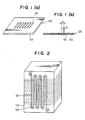
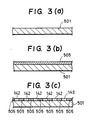
- the above-described type of electrical connection member 125 has a construction in which pins 121 made of electrically conductive material are buried in a sheet-like carrier made of electrical insulation resin 123.
- the illustrated electrical connection member 125 has heretofore been produced by the method shown in Fig. 2 (disclosed in, for example, U.S. Pat. No. 3,862,790).
- This method of producing the above-described type of electrical connection member comprises the steps of lacing, as shown in Fig. 2, conductor wire 124 around rods 122 which are disposed at a desired pitch in a staggered manner, the conductor wire 124 having a predetermined diameter and to be cut into the pins 121 which constitute part of each electrical connection member 125; molding this conductor wire 124 with the resin 123 having electrical insulation properties; curing the resin 123; and cutting the cured product into the sheet-like electrical connection members 125 each having a desired thickness.
- the above-described conventional method of producing electrical connection members has a number of problems.
- the electrically conducting portions are formed by utilizing the method of lacing conductor wire in a staggered manner, the density of the electrically conducting portions is limited.
- Another disadvantage of the electrical connection member produced by the aforesaid method is that, since the conductor wire which constitutes the electrically conducting portions is approximately equal in diameter to holes which retain the conductor wire in the resin layer of the electrical connection member, the conductor wire tends to easily come away from the resin layer. This disadvantage may lead to a deterioration in the reliability of electrical connection.
- a further disadvantage of the electrical connection member produced by the aforesaid method is that, since the surfaces of the sheet-like carrier made of the resin having electrical insulating properties are flush with the contact ends of the electrically conducting portions, it is difficult to achieve a reliable connection with electrical circuit parts.
- the contact ends of the electrically conducting portions be formed into a bump-like configuration.
- the surface of the resin carrier of the sheet-like electrical connection member be etched to expose electrically conductive members made from the conductor wire and the exposed conductive members be then melted either mechanically or thermally. Accordingly, it has been impossible to avoid the problem that the production process inevitably becomes a complicated one.
- It is still another object of the present invention is to provide a method of producing electrical connection members, comprising the steps of forming a carrier on a first electrically conductive member; forming holes in predetermined portions of the carrier by exposure and etching, thereby partially exposing a surface of the first electrically conductive member in the holes; etching the portions of the first electrically conductive member which are exposed in the respective holes formed in the carrier, thereby forming recesses in the first electrically conductive member so that each of the recesses has a diameter larger than the diameter of a corresponding one of the holes; filling the respective holes formed in the carrier with second electrically conductive members; and eliminating the first electrically conductive member from the carrier.
- An electrical connection member of the type produced by a method according to the present invention consists of a carrier made of an electrically insulating material and a plurality of electrically conductive members buried in the carrier, the electrically conductive members being partially exposed on the opposite surfaces of the carrier.
- the electrical connection member may further include a wiring pattern. This wiring pattern may be formed in the interior of the carrier or on either or both of the opposite surfaces of the carrier.
- electrical connection members of the type having a wiring pattern formed on either or both of the opposite surfaces of the carrier can be produced more easily than electrical connection members of the type having a wiring pattern formed in the interior of the carrier.
- the wiring pattern may be or may not be electrically connected to the individual electrically conductive members buried in the carrier. Moreover, the wiring pattern and the electrically conductive members may be electrically connected in the interior of the carrier or on either or both of the opposite surfaces of the carrier. In this case, it is possible to more easily produce electrical connection members of the type in which the wiring pattern and the electrically conductive members are electrically connected on either or both of the opposite surfaces of the carrier.
- the material of the wiring pattern is not limited to an electrically conductive metallic material, and any other kind of electrically conductive material may be employed.
- the connecting portions of electrical circuit parts may be connected to the contact ends (connecting portions) of the individual electrically conductive members, or they may be connected to the wiring pattern.
- the ends of the connecting portions of the respective electrically conductive members have a protruding configuration in order to achieve reliable connection with the electrical circuit parts and to prevent the electrically conductive members from coming away from the electrical connection member.
- Such an electrical connection member may be either of the single-layer type or of the multi-layer type, the latter consisting of two or more layers.
- the first electrically conductive member may have an electrically conductive material provided on at least one part of either of its opposite surfaces, or it may be made of electrically conductive material as a whole. Specifically, the whole of the first electrically conductive member may be made of a first electrically conductive material (for example, it may be formed from a sheet-like member made of the first electrically conductive material). Otherwise, it may have a construction in which the first electrically conductive material is provided on at least one part of a resin sheet. This first electrically conductive material may be selected from among materials which will be described later in the section "ELECTRICALLY CONDUCTIVE MEMBER". It is necessary, however, that the kind of first electrically conductive material differ from the kind of second electrically conductive material which forms the second electrically conductive members.
- the kind of material which forms a third electrically conductive member may be the same as the material which forms the first electrically conductive member.
- the kind of material which forms the second electrically conductive members may or may not be the same as the material which forms the third electrically conductive member.
- a resin having electrically insulating characteristics is applied to the first electrically conductive member made of the first electrically conductive material, thereby forming a carrier.
- the means of application may be selected arbitrarily.
- the resin having electrically insulating characteristics may be selected from among various materials which will be described later in the section "CARRIER". It is particularly desirable to employ a light-sensitive resin of the type which has electrically insulating characteristics and which can satisfy various requirements concerning formability, heat resistance, weather resistance, reliability (for example, the degree of shielding effect with respect to harmful electromagnetic waves), and the like. As an example, it is preferable that light-sensitive polyimide resin be used, but it is of course possible to employ any other kind of resin which can be cured when illuminated with light.
- a light-sensitive resin is used as the resin having electrically insulating characteristics
- the portions of the resin to be cured are illuminated with light (EXPOSURE).
- a photomask may be employed.
- the optically cured portion of the resin is eliminated by development and thus holes are iormed.
- the electrically conductive material which constitutes the first electrically conductive member is exposed through these holes.
- the above etching be continued until the diameters of recesses to be formed by this etching become larger than those of the corresponding holes formed in the carrier.
- the second electrically conductive members are filled into the respective holes in the carrier, the second electrically conductive members are also filled into these recesses, thereby forming bumps.
- etching liquid which etches the first electrically conductive material and yet which does not etch the resin constituting the carrier.
- the second electrically conductive members are filled into the recesses formed by etching. (These second electrically conductive members serve as electrically conductive members which constitute the connecting portions of the electrical connection member).
- the second electrically conductive members may be filled by, for example, plating, but another suitable method such as vapor deposition may also be employed.
- the material which forms the second electrically conductive members may be filled until their end surfaces become flush with or project above the outside surface of the formed carrier (that is, the surface of the carrier which is opposite to the surface carrying the first electrically conductive member).
- the electrically conductive material of the first electrically conductive member is eliminated by etching using an appropriate etching liquid.
- the etching liquid be of the kind which etches only the electrically conductive material of the first electrically conductive member and yet which does not etch the electrically conductive material of the second electrically conductive members.
- the wiring pattern may be provided on a surface of the carrier or on surfaces of the second electrically conductive members after the filling step described above has been completed. Incidentally, the wiring pattern may be provided either before or after the first electrically conductive member has been eliminated.
- the second electrically conductive members serve as electrically conductive members which constitute the connecting portions of the electrical connection member.
- the electrically conductive members may be made of any kind of material which exhibits electrical conductivity, and a metallic material is commonly employed. In place of a metallic material, a material which exhibits superconductivity may be used.
- gold be used as the metallic material.
- a suitable metal or metallic alloy other than gold may also be employed, and typical examples are Ag, Be, Ca, Mg, Mo, Ni, W, Fe, Ti, In, Ta, Zn, Cu, Al, Sn and Pb-Sn.
- metal or alloy material of an identical electrical connection member the same kind of metal may be present or metals of different kinds may be present.
- one metal or alloy member which constitutes part of the electrical connection member may be made of the same kind of metal or alloy, or it may be made of metals or alloys of different kinds.
- any other electrically conductive material other than a metal or alloy for example, a material consisting of a metallic material which contains at least an organic material or an inorganic material. Provided that sufficient electrical conductivity can be obtained, a composition of organic and inorganic materials may also be used.
- each of the electrically conductive members may be round, square, or similar.
- the diameters of the electrically conductive members are not limited to a specific value.
- such a diameter may be made greater than or less than 20 ⁇ m by taking into account the pitch of the connecting portions of the electrical circuit part.
- the exposed end surfaces of the electrically conductive members may be flush with or project above the outside surface of the carrier. These exposed end surfaces may be formed to project above either or both of the opposite surfaces of the carrier. If the bumps described above are formed on the opposite surfaces, it is possible to prevent the second electrically conductive members from coming away from the carrier and it is also possible to improve the state of connection with electrical circuit parts.
- the intervals between adjacent electrically conductive members may be equal to or narrower than the intervals between adjacent connecting portions of an electrical circuit part. If the former intervals are narrower than the latter intervals, it is possible to connect the electrical circuit part to the electrical connection member without the need for a positioning operation.
- the electrically conductive members need not be vertically arranged in the carrier. For example, they may be arranged in the carrier such that they run in an inclined state from one surface to the other surface of the carrier.
- the carrier used in the present invention may be made from a member consisting of an electrically insulating material.
- the organic material may be selected from among, for example, electrically insulating materials, and it is possible to employ any kind of light-sensitive resin such as thermosetting resin, ultraviolet-curing resin, or thermoplastic resin.
- the organic material may be selected from the group consisting of polyimide resin, polyphenylene sulfide resin, polyether sulfone resin, polyether imide resin, polysulfone resin, silicone resin, fluororesin, polycarbonate resin, polydiphenyl ether resin, polybenzyl imidazole resin, phenol resin, urea resin, melamine resin, alkyd resin, epoxy resin, polyamide-imide resin, polypropylene resin, polyvinyl chloride resin, polystryrene resin, methacrylate methyl resin, polyphenylene oxide resin, methacrylate plastics, vinylidene chloride resin, and similar kinds of resin or plastics.
- the light-sensitive polyimide resin is employed as the constituent material of the carrier, it is possible to provide an electrical connection member which is easy to form and which excels in heat resistance and weather resistance. Moreover, since the heat resistance of polyimide resin is particularly high, it is possible to easily achieve connection utilizing a metal or metallic alloy which is obtained by fusing the contacting surfaces of the electrical circuit part and the second electrically conductive members, as will be described later.
- the polyimide resin also has the effect of blocking harmful waves such as electromagnetic waves which would adversely affect electrical circuits.
- the light-sensitive resin may be selected from among, for example, polyimide resin, silicone resin, and similar kinds of resin.
- a resin of good heat conductivity be selected from the above resins since the heat generated in an electrical circuit part such as a semiconductor device can be dissipated through the resin. If a resin is selected which has a thermal expansion coefficient approximately equal to that of the circuit board of the electrical connection member and if at least one hole or a plurality of bubbles are formed in the organic material, it is possible to prevent the reliability of the device from deteriorating due to thermal expansion or thermal shrinkage.
- the metallic material or the alloy material may be selected from the group consisting of, for example, Ag, Cu, Au, Al, Be, Ca, Mg, Mo, Fe, Ni, Si, Co, Mn, W, Cr, Nb, Zr, Ti, Ta, Zn, Sn, and Pb-Sn.
- the inorganic material may be selected from the group consisting of, for example, SiO2, B2O3, Al2O3, Na2O, K2O, CaO, ZnO, BaO, PbO, Sb2O3, As2O3, La2O3, ZrOz2 BaO, P2O5, TiO2, MgO, SiC, BeO, BP, BN, AlN, B4C, TaC, TiB2, CrB2, TiN, Si3N4, Ta2O5, and other inorganic materials such as ceramics, diamond, glass, carbon, boron and the like.
- the carrier if a material of good heat conductivity is used for the carrier, the heat generated in electrical circuit parts or probe cards can be made to rapidly escape to the outside. Accordingly, an electrical circuit device of good heat dissipation properties is obtained. If a material having a thermal expansion coefficient close to that of an electrical circuit part is used for the carrier, the thermal expansion coefficient of the carrier approximates that of the electrical circuit part. Accordingly, it is possible to prevent any phenomena which may deteriorate the reliability of the electrical circuit device, such as cracks in the electrical circuit part or variations in the characteristics thereof which may be caused during the application of heat. It is, therefore, possible to provide a highly reliable electrical circuit member.
- the carrier if a material having a high magnetic shielding effect is used for the carrier, it is possible, to reduce the amount of electromagnetic noise which may leak from the electrical circuit part to the outside. It is also possible to reduce the amount of electromagnetic noise which may enter the electrical circuit part from the outside.
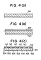
- a first electrically conductive member 501 is initially prepared.
- the first electrically conductive member 501 is made from a metallic sheet having characteristics suitable for such a conductive member.
- the first electrically conductive member 501 is hereinafter referred to also as the "metallic sheet 501").
- the carrier layer 505 is formed by applying a coat of light-sensitive resin (polyimide resin (PI)) to the metallic sheet 501 by means of a spinner and prebaking this coat of light-sensitive resin. Subsequently, the carrier layer 505 is illuminated with light through a photomask (for the purpose of exposure) and is then subjected to development.
- the portions of the polyimide resin which have been exposed to light are not removed during the development and thus form the carrier, while the portions of the polyimide resin which have not been illuminated with light are removed by the development to form holes 142.
- the processing temperature is increased to convert the polyimide resin into an imide compound.
- the portions of the metallic sheet 501 which are exposed at the bottoms of the respective holes 142 formed in the above step are etched to form recesses 502 in the metallic sheet 501. It is preferable for this etching to be continued until the diameter of each recess 502 exceeds the diameter of the corresponding hole 142 formed in the carrier.
- second electrically conductive material which constitutes a second electrically conductive members 150 is charged into holes 142.
- gold is used as the second electrically conductive material 150 and is charged into the holes 142 by a plating process. Gold plating is continued until bumps are formed on the exposed surface of the carrier layer 505.
- gold plating may be stopped, when the external surfaces of the second electrically conductive members 150 become flush with the exposed surface of the carrier layer 505.
- the metallic sheet 501 is removed by metal etching.
- the second electrically conductive material or gold 150 charged into the holes 142 constitutes electrically conductive members 107
- the carrier layer 505 made of polyimide resin constitutes a carrier 111.
- the thickness c of the carrier 111 is approximately 10 ⁇ m
- the pitch a and the diameter b of each of the electrically conductive members 107 are approximately 40 ⁇ m and approximately 20 ⁇ m, respectively.
- the amount of projection of each bump is several microns on either side of the carrier 111.
- the method of producing the electrical connection member 125 described above need not necessary include the step, shown in Fig. 3(d), of etching the metallic sheet 501. This is because, if the electrically conductive members 107 of the electrical connection member 125 are formed such as to be exposed flush with either surface of the carrier 111, the electrically conductive members 107 can achieve sufficient electrical connection with the connecting portions of another electrical circuit part.
- each recess 502 has a greater diameter than the corresponding hole 142 formed in the carrier 111, thereby forming the contact ends of the electrically conductive members 107 into a protruding configuration.
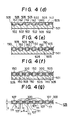
- a method of producing electrical connection members in accordance with this embodiment includes the process steps shown in Figs. 4(a) to 4(e) which are carried out in a manner similar to that used in the aforesaid embodiment 1.
- the step of forming a wiring pattern 300 on the surface of the carrier layer 505 which is opposite to the other surface carrying the metallic sheet 501 is added after the step, shown in Fig. 4(e), of forming the second electrically conductive members 150.
- the wiring pattern 300 is formed in accordance with a desired configuration by depositing an electrically conductive material to constitute a wiring pattern made of, for example, copper on both the carrier layer 505 and the second electrically conductive members 150 by means of vapor deposition or sputtering, providing patterning by etching unnecessary portions, and depositing gold on this wiring pattern by plating, vapor deposition or the like.
- the metallic sheet 501 is etched with a liquid which is able to etch the metallic sheet 501 alone, thereby forming an electrical connection member having the desired wiring pattern.
- Such a wiring pattern may be formed not by the above-described method but by various known methods of forming wiring patterns.
- the electrical connection member 125 thus produced has a construction in which the wiring pattern is formed on one surface alone.
- the electrical connection member 125 With the above-described embodiment, it is possible to form the electrical connection member 125 with a wiring pattern formed on just one of its surfaces. If it is necessary to form wiring patterns on the opposite surfaces of the electrical connection member 125, the following method may be utilized.
- the above-described method may be employed to form the wiring pattern 300 on the surface of the carrier layer 505 to which the metallic sheet 501 has been bonded.
- wiring patterns may be formed on the opposite surfaces of this electrical connection member 125.
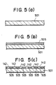
- the method, shown in Figs. 5(a) to 5(h), of producing such an electrical connection member 125 includes process steps (Figs. 5(a) to 5(e)) which are the same as the corresponding process steps used in the method shown in each of Embodiments 1 and 2.
- a method which is similar to the method shown in Embodiment 2 of forming a wiring pattern is employed to form the wiring pattern 300 in a desired area on each of the second electrically conductive members exposed through a first carrier layer.
- Fig. 5(e) after the step, shown in Fig. 5(e), of forming the second electrically conductive members has been completed, a method which is similar to the method shown in Embodiment 2 of forming a wiring pattern is employed to form the wiring pattern 300 in a desired area on each of the second electrically conductive members exposed through a first carrier layer.
- a second carrier layer made of light-sensitive polyimide resin is formed to cover the wiring pattern 300.
- exposure and development of the second carrier layer are effected by process steps which are respectively similar to those shown in Figs. 5(c) and 5(e), thereby forming desired holes, and third electrically conductive members are filled into the holes for providing electrical connection with the second electrically conductive members or the wiring pattern exposed in the holes.
- the metallic sheet 501 is removed by etching, thus preparing a multi-layer type of electrical connection member 125.
- the multi-layer type electrical connection member 125 produced by this embodiment constitutes an electrical connection member which has a single-layer wiring pattern in its interior.
- polyimide resin is preferably used as the constituent material of the first and second carrier layers which constitutes part of the electrical connection member 125.
- Heating for the purpose of converting the first carrier layer into an imide compound is not carried out in the step shown in Fig. 5(c) in this embodiment; such heating is effected in either of the steps shown in Figs. 5(g) and 5(h). Accordingly, no substantial interface layer is formed between the first carrier layer formed in the step of Fig. 5(b) and the second carrier layer formed in the step of Fig. 5(f), whereby it is possible to form the first and second carrier layers as a substantially single carrier layer.
- two or more layers of wiring patterns may be formed in the interior of the electrical connection member 125 by repeating the steps of Figs. 5(f) to 5(g).
- such a wiring pattern may be formed on either or both of the opposite surfaces of the carrier, as described previously in connection with Embodiment 2.
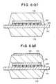
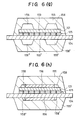
- a semiconductor device 101 serving as an electrical circuit part, a circuit board 104 and an electrical connection member 125 for electrically connecting the elements 101 and 104 were initially prepared.
- the semiconductor device 101 and the circuit board 104 which were used in this example had a multiplicity of connecting portions 102 and 105, respectively.
- the connecting portions 102 and 105 were electrically insulated by electrical insulation films 103 and 106, respectively.
- the connecting portions 102 of the semiconductor device 101 consist of electrical conductors which are exposed at locations corresponding to the respective connecting portions 105 of the circuit board 104 and corresponding connecting portions 108 and 109 of the electrical connection member 125.
- the semiconductor device 101, the circuit board 104 and the electrical connection member 125 were positioned so that the connecting portions 102 of the semiconductor device 101 corresponded to the respective connecting portions 108 of the electrical connection member 125 or so that the connecting portions 105 of the circuit board 104 corresponded to the connecting portions 109 of the electrical connection member 125.
- the connecting portions 102 of the semiconductor device 101 are connected to the corresponding connecting portions 108 of the electrical connection member 125 by means of a metal and/or metallic alloy formed by fusing the contacting surfaces of the connecting portions 102 and 108, while the connecting portions 105 of the circuit board 104 are connected to the corresponding connecting portions 109 of the electrical connection member 125 by means of a metal and/or metallic alloy formed by fusing the contacting surfaces of the connecting portions 105 and 109.
- these elements 101, 125 and 104 were connected as shown in Fig. 6(b) to prepare an electrical circuit member.
- the following three method are available.
- a metal and/or metallic alloy is formed by fusing the contacting surfaces of the connecting portions 102 of the semiconductor device 101 and the connecting portions 108 of the electrical connection member 125 and, at the same time, a metal and/or metallic alloy is formed by fusing the contacting surfaces of the connecting portions 105 of the circuit board 104 and the connecting portions 109 of the electrical connection member 125. In this way, the elements 101, 125 and 104 are connected at the same time.
- the semiconductor device 101 and the electrical connection member 125 are positioned with respect to each other, and the connecting portions 102 of the semiconductor device 101 and the corresponding connecting portions 108 of the electrical connection member 125 are connected by,means of a metal and/or metallic alloy formed by fusing the contacting surfaces of the connecting portions 102 and 108.
- the circuit board 104 is positioned with respect to the electrical connection member 125, and the connecting portions 109 of the electrical connection member 125 and the connecting portions 105 of the circuit board 104 are connected by means of a metal and/or metallic alloy formed by fusing the contacting surfaces of the connecting portions 109 and 105.
- the circuit board 104 and the electrical connection member 125 are initially positioned with respect to each other, and the connecting portions 105 of the circuit board 104 and the connecting portions 109 of the electrical connection member 125 are connected by means of a metal and/or metallic alloy formed by fusing the contacting surfaces of the connecting portions 105 and 109. Then, the semiconductor device 101 is positioned with respect to the electrical connection member 125, and the connecting portions 108 of the electrical connection member 125 and the connecting portions 102 of the semiconductor device 101 are connected by means of a metal and/or metallic alloy formed by fusing the contacting surfaces of the connecting portions 108 and 102.
- a typical example of the method of forming such a metal or metallic alloy is to bring the connecting ends of an electrical connection member into contact with corresponding connecting portions of a desired electrical circuit part and apply heat at an appropriate temperature.
- diffusion or the like of atoms occurs in the vicinity of each contacting portion due to heating, and the thus-diffused portions are transformed into the metal or metallic alloy, thereby forming a layer of metal or metallic alloy.
- the heating temperature be set to 200-350°C.
- the heating method may be one kind selected from among internal heating methods such as thermocompression bonding, ultrasonic heating, high-frequency induction heating, high-frequency dielectric heating, microwave heating, and the like, or from among various other external heating methods, or it may be a combination of two or more kinds selected from among these heating methods.
- the connecting portions are connected by heating them either directly or indirectly.
- the melting point of the metal or metallic alloy layer formed by fusing the contacting surfaces of the electrical connection member and an electrical circuit part to be removably connected be made lower than the melting point of the metal or metallic alloy layer formed by fusing the electrical connection member and an electrical circuit part to be nonremovably connected. If these melting points are selected in this manner, it is possible to remove only a desired removable electrical circuit part without exerting adverse influence, such as physical damage, on the connecting portions of the nonremovable electrical circuit parts.
- the "removable connection” embraces the above form of connection as well.
- individual electrical circuit parts are connected via the electrical connection member by the formation of the metal and/or metallic alloy layer described above. Accordingly, since the electrical circuit parts are connected to each other firmly (with high strength) and reliably, it is possible to provide an electrical circuit device having connections of reduced resistance and of uniform resistance characteristics, improved mechanical strength, and an extremely low failure rate.
- the electrical circuit parts of the electrical circuit member thus produced were sealed with a sealing compound in the manner shown in Fig. 6(c).
- a sealing compound employed was thermoplastic resin and the sealing method was injection molding.
- thermoplastic resin may be selected from the group consisting of, for example, polyimide resin, polyphenylene sulfide resin, polyether sulfone resin, polyether imide resin, polysulfone resin, fluororesin, polycarbonate resin, polydiphenyl ether resin, polybenzyl imidazole resin, polyamide imide resin, polypropylene resin, polyvinyl chloride resin, polystryrene resin, methacrylate methyl resin and similar kinds of resin.
- the above sealing compound may be selected from the above noted group or it may be of the type in which one or more materials selected from among metal, alloy and inorganic material in the form of powder, fibers, plate-like grains, rod-like grains, or spherical grains are dispersed in any of the aforesaid thermoplastic resins.
- This dispersion may be effected by adding an arbitrary material in the form of powder, fibers, plate-like grains, rod-like grains, or spherical grains to a selected resin and agitating the mixture.
- another arbitrary method may be employed to disperse, in a selected resin, a material in the form of powder, fibers, plate-like grains, rod-like grains, or spherical grains.
- the aforesaid metal or alloy may be selected from the group consisting of, for example, Ag, Cu, Au, Al, Be, Ca, Mg, Mo, Fe, Ni, Si, Co, Mn and W.
- the aforesaid inorganic material may be selected from the group consisting of, for example, SiO2, B2O3, Al2O3, Na2O, K2O, CaO, ZnO, BaO, PbO, Sb2O3, As2O5, La2O3, ZrO2, BaO, P2O3, TiO2, MgO, SiC, BeO, BP, BN, AlN, B4C, TaC, TiB2, CrB2, TiN, Si3N4, Ta2O5, and other inorganic materials such as ceramics, diamond, glass, carbon, boron, and the like.
- the size and the configuration of powder particles, fibers, plate-like grains, rod-like grains, or spherical grains to be dispersed may be arbitrarily selected. Moreover, the position of dispersion in the insulating resin and the amount of material to be dispersed may also be arbitrarily determined.
- the powder, fibers, plate-like grains, rod-like grains or spherical grains may be or may not be exposed to the outside of the insulating resin. In addition, the powder, fibers, plate-like grains, rod-like grains, or spherical grains may be or may not be in contact with one another.
- the thermal expansion coefficient of the sealing compound approximates that of the electrical circuit part.
- Fig. 6(d) shows an example in which a 0.1 mm thick sheet 151 made of stainless steel is bonded to the surface of a sealing material 170 of the electrical circuit member of Fig. 6(c).
- Fig. 6(e) shows another example in which the 0.1 mm thick sheet 151 made of stainless steel is bonded to the surface of the semiconductor device 101 which is opposite to the electrical connection member 125 in the electrical circuit member of Fig. 6(c).
- the sheet 151 is bonded to the semiconductor device 101 alone.
- Fig. 6(f) shows still another example in which the 0.1 mm thick sheet 151 made of stainless steel is disposed in the vicinity of the semiconductor device 101 in the electrical circuit member shown in Fig. 6(c).
- the thickness of the stainless sheet is preferably 0.05-0.5 mm.
- the bonding method is not limited to a specific method, and various methods can be employed.
- the sheet may be bonded by using an adhesive or the like.
- the sheet is made of metal such as stainless steel, a ceramic of good heat conductivity, carbon, diamond or the like, the heat generated from an electrical circuit part can be rapidly dissipated to the exterior. Accordingly, it is possible to provide an electrical circuit device having good heat-dissipation characteristics. If the sheet is made of metal, the penetration of external noise can be prevented and it is therefore possible to make the device insusceptible to the influence of external noise. Moreover, since electromagnetic noise generated from electrical circuit parts can be blocked, it is possible to provide an electrical circuit member of good characteristics without high noise.
- the above-described sheet is provided on the outside surface of the sealing portion or is buried therein. Accordingly, even if internal stress occurs in the electrical circuit member or external stress is applied to it, it is possible to suppress stress concentration and, hence, prevent cracks or the like which may occur due to stress concentration.
- the above sheet also serves as protecting means for protecting the electrical circuit parts from the influences of the exterior. Accordingly, it is possible to prevent water or other foreign matter from easily penetrating the electrical circuit parts, whereby the reliability of the electrical circuit member can be improved.
- Fig. 6(g) shows yet another example in which each of the circuit board 104 and the semiconductor device 101 is sealed with a cap in the electrical circuit member shown in Fig. 6(c).
- seal(ed) with a cap means that a cap is employed to wrap an electrical circuit part to seal the same with a certain cavity remaining in the interior of the cap.
- the cap may be provided on only one of the electrical circuit parts to be sealed, or a plurality of caps may be provided on individual electrical circuit parts to be sealed.
- the caps used in this example are denoted by 155 and 155′, respectively.
- each of the caps 155 and 155′ has two recesses formed in its interior.
- the recesses of the cap 155 form cavities 158 and those of the cap 155′ form cavities 158′.
- a projecting portion 159 abuts against the facing surface (reverse surface) of the semiconductor device 101 while a projecting portion 159′ abuts against the facing surface (reverse surface) of the circuit board 104.
- the semiconductor device 101 and the circuit board 104 are firmly held against the electrical connection member 125 by the projecting portions 159 and 159′, respectively.
- caps 155 and 155′ are bonded to each other with an adhesive.
- each of the caps 155 and 155′ is made of material having good noise filtering characteristics, particularly iron or an alloy thereof, it is possible to provide an electrical circuit member which has a further improved function of shielding the incorporated electrical circuit parts from external noise.
- Fig. 6(h) shows another example in which the semiconductor device 101 and the circuit board 104 of the electrical circuit member of Fig. 6(c) are sealed with the caps 155 and 155′, respectively, in a similar manner to that used in the example of Fig. 6(g), but in which two adjustment members 156 are provided for adjusting the dimension of each of the electrical circuit parts in the direction of the height thereof.
- One of the adjustment members 156 is interposed between the semiconductor device 101 and the cap 155, the other between the circuit board 104 and the cap 155′.
- the interposition of the adjustment members 156 between the cap 155 and one of the electrical circuit parts and between the cap 155′ and the other electrical circuit part makes it possible to efficiently assemble the electrical circuit member even if individual electrical circuits differ in height.
- Each of the adjustment members may be made of metallic material, inorganic material, or organic material, and it is desirable to use a material having elasticity.
- the adjustment member may have any configuration that allows the dimension of each electrical circuit part to be adjusted in the direction of the height thereof.
- each of the examples described above employs the electrical connection member produced in accordance with Embodiment 1.
- the electrical connection member produced in accordance with either of Embodiments 1 and 2 can also be used to provide an electrical circuit member having reliability which is as high as the reliability of the above-described electrical circuit member.
- the connecting portions of each electrical circuit part can be provided along its end portion at high density. Accordingly, it is possible to increase the number of connecting portions to be provided at the end portion, whereby the density of connecting portions can be made high.
- the thickness of the electrical connection member can be made small, it is possible to reduce the total thickness of the electrical circuit member.
- the electrical connection member 125 produced by the method of Embodiment 1 is utilized, but W or an alloy thereof is used for the second electrically conductive members and one side of each bump is formed into an acute configuration.
- predetermined portions are plated with solder after the second electrically conductive members have been formed by the process step shown in Fig. 3(e).
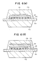
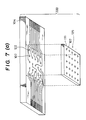
- the circuit board 104 as an electrical circuit part and the electrical connection member 125, which constitutes the probing portion of the probe card, are initially prepared.
- the circuit board used in this example has a multiplicity of connecting portions 102 in its interior.
- the connecting portions 102 of the circuit board 104 consist of electrically conductive members which are exposed at locations corresponding to the respective connecting portions 108 of the electrical connection member 125.
- the positions of the circuit board 104 and the electrical connection member 125 are initially adjusted so that the connecting portions 102 correspond to the connecting portions 108 as shown in Fig. 7(b). Then, the connecting portions 102 (in this example, made of Cu and plated with solder) of the circuit board 104 and the connecting portions 108 (in this example, made of W and plated with solder) of the electrical connection member 125 are bonded by brazing material.
- a probe card 200 is prepared in this manner.
- the semiconductor device 101 is employed as an electrical part to be measured.
- the semiconductor device 101 has connecting portions which are arranged at a pitch of 40 ⁇ m.
- the positions of the semiconductor device 101 and the electrical connection member 125 are adjusted so that the connecting portions 105 correspond to the connecting portions 109. Then, the connecting portions 105 (in this example, made of Al) of the semiconductor device 101 and the connecting portions 109 (in this example, made of W) of the electrical connection member 125 are bonded as shown in Fig. 7(c). In this state, the electrical characteristics of the semiconductor device 101 are measured.
- the connection formed in this step is a temporary connection, and after the measurement has been completed, the semiconductor device 101 can be easily removed from the probe card 200. Accordingly, each time measurement is taken, the semiconductor device 101 can be attached to and detached from the probe card 200.
- Figs. 8(a), 8(b) and 8(c) diagrammatically show another form of the probe card 200 produced in Example 2.
- the probe card 200 produced in Example 2 includes an electrical connection member, denoted by 125, having a surface with a wiring pattern formed by a method similar to the method explained in Embodiment 2, and further include a reinforcement plate 305 provided on the electrical connection member 125.
- the electrical connection member 125 used in Example 3 is produced by the method explained in Embodiment 2. However, in the step, shown in Fig. 4(e), of forming the second electrically conductive members 150, none of the portions of the second electrically conductive members 150 which are exposed on the side opposite to the metallic sheet 501 is formed into a bump and these exposed portions are made approximately flush with the corresponding surface of the carrier 111.
- the second electrically conductive member 150 prepared in the process step shown in Fig. 4(e) is formed utilizing Au plating, W plating or W-alloy plating, followed by solder plating.
- the probe card 200 having the above-described construction is connected to the semiconductor device 101 which is an electrical circuit part to be measured, and the electrical characteristics of the semiconductor device 101 are measured by a method similar to that shown in Example 2.
- the electrical connection member used in each of Examples 2 and 3 is not limited to the above-described specific example, and it is possible to use any of the electrical connection members which are produced by the methods shown in Embodiments 1 to 3.
- a probe card utilizing an electrical connection member of the type achieved in accordance with the present invention makes it possible to facilitate the measurement of electrical characteristics, such as current, voltage, frequency characteristics and the like of electrical circuit parts of the type in which connecting portions are provided on their outer edge portions or in their interiors. Moreover, since the electrically conductive members of the electrical connection member can be formed at a narrow pitch, the number of connecting portions can be increased and it is, therefore, possible to measure electrical parts of the type having a multiple-pin connection.
- the production method according to the present invention utilizes a process for applying a coat of resin, it is possible to produce very thin electrical connection members.
- the longitudinal size of each electrically conductive member in the electrical connection member can be made small, it is possible to achieve stable connections whose electrical resistance and stray capacitance are reduced and which can reduce the level of noise coming from the exterior.
- holes to be filled with the electrically conductive members are formed by photolithography, it is possible to easily increase the density of connecting portions of the electrical connection member. Since the operation of positioning electrical circuit parts with respect to the electrical connection member can be simplified, it is also possible to eliminate complicated positioning operation.
- polyimide resin is used as resin which varies in hardness when illuminated with light, it is possible to produce highly reliable electrical connection members which excel in heat resistance, weather resistance, and shielding effect with respect to harmful electromagnetic waves.
- each of the second electrically conductive members can be easily formed into a bump-like configuration. Accordingly, it is possible to prevent the second electrically conductive members from accidentally coming away from the carrier and it is also possible to achieve stable connections between electrical circuit parts and the second electrically conductive members.
- a method of producing electrical connection members comprises the steps of forming a carrier on a first electrically conductive member; forming holes in predetermined portions of the carrier by exposure and etching, thereby partially exposing a surface of the first electrically conductive member in the holes; etching the portions of the first electrically conductive member which are exposed in the respective holes, thereby forming recesses in the first electrically conductive member so that each of the recesses has a diameter larger than the diameter of a corresponding one of the holes; filling the respective holes formed in the carrier with second electrically conductive members; and eliminating the first electrically conductive member from the carrier.
Landscapes
- Manufacturing Of Electrical Connectors (AREA)
- Wire Bonding (AREA)
- Printing Elements For Providing Electric Connections Between Printed Circuits (AREA)
- Measuring Leads Or Probes (AREA)
- Testing Or Measuring Of Semiconductors Or The Like (AREA)
Applications Claiming Priority (2)
| Application Number | Priority Date | Filing Date | Title |
|---|---|---|---|
| JP133401/88 | 1988-05-31 | ||
| JP63133401A JP2702507B2 (ja) | 1988-05-31 | 1988-05-31 | 電気的接続部材及びその製造方法 |
Publications (3)
| Publication Number | Publication Date |
|---|---|
| EP0344720A2 true EP0344720A2 (de) | 1989-12-06 |
| EP0344720A3 EP0344720A3 (de) | 1991-10-16 |
| EP0344720B1 EP0344720B1 (de) | 1998-04-08 |
Family
ID=15103885
Family Applications (1)
| Application Number | Title | Priority Date | Filing Date |
|---|---|---|---|
| EP89109747A Expired - Lifetime EP0344720B1 (de) | 1988-05-31 | 1989-05-30 | Verfahren zur Herstellung elektrischer Verbindungsteile |
Country Status (4)
| Country | Link |
|---|---|
| US (1) | US4926549A (de) |
| EP (1) | EP0344720B1 (de) |
| JP (1) | JP2702507B2 (de) |
| DE (1) | DE68928633T2 (de) |
Cited By (3)
| Publication number | Priority date | Publication date | Assignee | Title |
|---|---|---|---|---|
| EP0501357A1 (de) * | 1991-02-25 | 1992-09-02 | Canon Kabushiki Kaisha | Elektrischer Verbindungsteil und sein Herstellungsverfahren |
| EP0501361A1 (de) * | 1991-02-25 | 1992-09-02 | Canon Kabushiki Kaisha | Elektrischer Verbindungskörper und Herstellungsverfahren dafür |
| EP0504614A1 (de) * | 1991-02-22 | 1992-09-23 | Canon Kabushiki Kaisha | Elektrischer Verbindungskörper und Herstellungsverfahren dafür |
Families Citing this family (42)
| Publication number | Priority date | Publication date | Assignee | Title |
|---|---|---|---|---|
| US5502889A (en) * | 1988-06-10 | 1996-04-02 | Sheldahl, Inc. | Method for electrically and mechanically connecting at least two conductive layers |
| US5798780A (en) * | 1988-07-03 | 1998-08-25 | Canon Kabushiki Kaisha | Recording element driving unit having extra driving element to facilitate assembly and apparatus using same |
| US5160779A (en) * | 1989-11-30 | 1992-11-03 | Hoya Corporation | Microprobe provided circuit substrate and method for producing the same |
| US5135606A (en) * | 1989-12-08 | 1992-08-04 | Canon Kabushiki Kaisha | Process for preparing electrical connecting member |
| US5379515A (en) * | 1989-12-11 | 1995-01-10 | Canon Kabushiki Kaisha | Process for preparing electrical connecting member |
| US5145552A (en) * | 1989-12-21 | 1992-09-08 | Canon Kabushiki Kaisha | Process for preparing electrical connecting member |
| US5819406A (en) * | 1990-08-29 | 1998-10-13 | Canon Kabushiki Kaisha | Method for forming an electrical circuit member |
| DE69216658T2 (de) * | 1991-02-25 | 1997-08-07 | Canon Kk | Vorrichtung und Verfahren zur Verbindung elektrischer Bauelemente |
| US5379191A (en) * | 1991-02-26 | 1995-01-03 | Microelectronics And Computer Technology Corporation | Compact adapter package providing peripheral to area translation for an integrated circuit chip |
| US5306872A (en) * | 1991-03-06 | 1994-04-26 | International Business Machines Corporation | Structures for electrically conductive decals filled with organic insulator material |
| US5108541A (en) * | 1991-03-06 | 1992-04-28 | International Business Machines Corp. | Processes for electrically conductive decals filled with inorganic insulator material |
| US5116459A (en) * | 1991-03-06 | 1992-05-26 | International Business Machines Corporation | Processes for electrically conductive decals filled with organic insulator material |
| US5338900A (en) * | 1991-03-06 | 1994-08-16 | International Business Machines Corporation | Structures for electrically conductive decals filled with inorganic insulator material |
| US5519332A (en) * | 1991-06-04 | 1996-05-21 | Micron Technology, Inc. | Carrier for testing an unpackaged semiconductor die |
| US5129833A (en) * | 1991-06-26 | 1992-07-14 | Amp Incorporated | Low-force, high-density gel connector |
| US5515604A (en) * | 1992-10-07 | 1996-05-14 | Fujitsu Limited | Methods for making high-density/long-via laminated connectors |
| US5727310A (en) * | 1993-01-08 | 1998-03-17 | Sheldahl, Inc. | Method of manufacturing a multilayer electronic circuit |
| US5387329A (en) * | 1993-04-09 | 1995-02-07 | Ciba Corning Diagnostics Corp. | Extended use planar sensors |
| US5428190A (en) * | 1993-07-02 | 1995-06-27 | Sheldahl, Inc. | Rigid-flex board with anisotropic interconnect and method of manufacture |
| US5527998A (en) * | 1993-10-22 | 1996-06-18 | Sheldahl, Inc. | Flexible multilayer printed circuit boards and methods of manufacture |
| US5455390A (en) * | 1994-02-01 | 1995-10-03 | Tessera, Inc. | Microelectronics unit mounting with multiple lead bonding |
| US5912597A (en) * | 1994-03-31 | 1999-06-15 | Canon Kabushiki Kaisha | Printed circuit board |
| JP3363651B2 (ja) * | 1994-04-21 | 2003-01-08 | キヤノン株式会社 | プリント配線板およびその設計方法 |
| JP2984205B2 (ja) * | 1996-01-10 | 1999-11-29 | 日東電工株式会社 | 異方導電フィルム |
| JP3376218B2 (ja) * | 1996-08-30 | 2003-02-10 | キヤノン株式会社 | 回路基板接続装置 |
| US6133072A (en) | 1996-12-13 | 2000-10-17 | Tessera, Inc. | Microelectronic connector with planar elastomer sockets |
| JPH10282144A (ja) * | 1997-04-07 | 1998-10-23 | Micronics Japan Co Ltd | 平板状被検査体試験用プローブユニット |
| JPH1123615A (ja) | 1997-05-09 | 1999-01-29 | Hitachi Ltd | 接続装置および検査システム |
| JPH1127859A (ja) | 1997-06-30 | 1999-01-29 | Nec Corp | 電源回路 |
| TW396462B (en) * | 1998-12-17 | 2000-07-01 | Eriston Technologies Pte Ltd | Bumpless flip chip assembly with solder via |
| US6036809A (en) * | 1999-02-16 | 2000-03-14 | International Business Machines Corporation | Process for releasing a thin-film structure from a substrate |
| US6627998B1 (en) * | 2000-07-27 | 2003-09-30 | International Business Machines Corporation | Wafer scale thin film package |
| US6840777B2 (en) | 2000-11-30 | 2005-01-11 | Intel Corporation | Solderless electronics packaging |
| US6694846B2 (en) * | 2002-02-28 | 2004-02-24 | Shimano Inc. | Bicycle pedal |
| TWI337935B (en) | 2003-06-06 | 2011-03-01 | Sumitomo Electric Industries | Production method for drilled porous resin substrate, and making the inner-wall of penetrated hole of the porous resin substrate conductive |
| JP2005340687A (ja) * | 2004-05-31 | 2005-12-08 | Fujitsu Ltd | 積層基板及びその製造方法、かかる積層基板を有する電子機器 |
| JP4380466B2 (ja) | 2004-08-23 | 2009-12-09 | 住友電気工業株式会社 | 穿孔された多孔質樹脂基材及び穿孔の内壁面を導電化した多孔質樹脂基材の製造方法 |
| JP4665848B2 (ja) * | 2006-03-15 | 2011-04-06 | 日立電線株式会社 | コネクタ構造 |
| US7425134B1 (en) * | 2007-05-21 | 2008-09-16 | Amphenol Corporation | Compression mat for an electrical connector |
| JP5588851B2 (ja) * | 2010-12-14 | 2014-09-10 | 株式会社日本マイクロニクス | 電気的接続装置及びその製造方法 |
| JP2012233723A (ja) * | 2011-04-28 | 2012-11-29 | Micronics Japan Co Ltd | プローブ装置及びプローブユニット |
| JP6520343B2 (ja) * | 2015-04-17 | 2019-05-29 | 大日本印刷株式会社 | 電極シートおよび電極シートの製造方法 |
Family Cites Families (15)
| Publication number | Priority date | Publication date | Assignee | Title |
|---|---|---|---|---|
| US2961746A (en) * | 1956-06-18 | 1960-11-29 | Aladdin Ind Inc | Printed circuits |
| US3193789A (en) * | 1962-08-01 | 1965-07-06 | Sperry Rand Corp | Electrical circuitry |
| US3541222A (en) * | 1969-01-13 | 1970-11-17 | Bunker Ramo | Connector screen for interconnecting adjacent surfaces of laminar circuits and method of making |
| US3778900A (en) * | 1970-09-04 | 1973-12-18 | Ibm | Method for forming interconnections between circuit layers of a multi-layer package |
| US3680037A (en) * | 1970-11-05 | 1972-07-25 | Tech Wire Prod Inc | Electrical interconnector |
| US3971610A (en) * | 1974-05-10 | 1976-07-27 | Technical Wire Products, Inc. | Conductive elastomeric contacts and connectors |
| US4050756A (en) * | 1975-12-22 | 1977-09-27 | International Telephone And Telegraph Corporation | Conductive elastomer connector and method of making same |
| US4067945A (en) * | 1976-03-24 | 1978-01-10 | Essex International, Inc. | Method of making a multi-circuit electrical interconnector |
| US4240198A (en) * | 1979-02-21 | 1980-12-23 | International Telephone And Telegraph Corporation | Method of making conductive elastomer connector |
| JPS55138294A (en) * | 1979-04-11 | 1980-10-28 | Matsushita Electric Industrial Co Ltd | Method of forming through hole connector |
| US4480288A (en) * | 1982-12-27 | 1984-10-30 | International Business Machines Corporation | Multi-layer flexible film module |
| JPS6059683A (ja) * | 1983-09-10 | 1985-04-06 | ジェイエスアール株式会社 | コネクタ−の製造方法 |
| DK291184D0 (da) * | 1984-06-13 | 1984-06-13 | Boeegh Petersen Allan | Fremgangsmaade og indretning til test af kredsloebsplader |
| JPS61239576A (ja) * | 1985-04-16 | 1986-10-24 | シチズン時計株式会社 | コネクタ−の製造方法 |
| US4628406A (en) * | 1985-05-20 | 1986-12-09 | Tektronix, Inc. | Method of packaging integrated circuit chips, and integrated circuit package |
-
1988
- 1988-05-31 JP JP63133401A patent/JP2702507B2/ja not_active Expired - Fee Related
-
1989
- 1989-05-30 US US07/358,269 patent/US4926549A/en not_active Expired - Lifetime
- 1989-05-30 EP EP89109747A patent/EP0344720B1/de not_active Expired - Lifetime
- 1989-05-30 DE DE68928633T patent/DE68928633T2/de not_active Expired - Fee Related
Cited By (8)
| Publication number | Priority date | Publication date | Assignee | Title |
|---|---|---|---|---|
| EP0504614A1 (de) * | 1991-02-22 | 1992-09-23 | Canon Kabushiki Kaisha | Elektrischer Verbindungskörper und Herstellungsverfahren dafür |
| EP0805493A3 (de) * | 1991-02-22 | 1998-02-04 | Canon Kabushiki Kaisha | Elektrischer Verbindungskörper und Herstellungsverfahren dafür |
| US5860818A (en) * | 1991-02-22 | 1999-01-19 | Canon Kabushiki Kaisha | Electrical connecting member |
| US6511607B1 (en) | 1991-02-22 | 2003-01-28 | Canon Kabushiki Kaisha | Method of making an electrical connecting member |
| EP0501357A1 (de) * | 1991-02-25 | 1992-09-02 | Canon Kabushiki Kaisha | Elektrischer Verbindungsteil und sein Herstellungsverfahren |
| EP0501361A1 (de) * | 1991-02-25 | 1992-09-02 | Canon Kabushiki Kaisha | Elektrischer Verbindungskörper und Herstellungsverfahren dafür |
| US5323535A (en) * | 1991-02-25 | 1994-06-28 | Canon Kabushiki Kaisha | Electrical connecting member and method of manufacturing the same |
| US5600884A (en) * | 1991-02-25 | 1997-02-11 | Canon Kabushiki Kaisha | Method of manufacturing electrical connecting member |
Also Published As
| Publication number | Publication date |
|---|---|
| JPH0249385A (ja) | 1990-02-19 |
| JP2702507B2 (ja) | 1998-01-21 |
| EP0344720A3 (de) | 1991-10-16 |
| DE68928633D1 (de) | 1998-05-14 |
| DE68928633T2 (de) | 1998-09-17 |
| US4926549A (en) | 1990-05-22 |
| EP0344720B1 (de) | 1998-04-08 |
Similar Documents
| Publication | Publication Date | Title |
|---|---|---|
| US4926549A (en) | Method of producing electrical connection members | |
| US5216807A (en) | Method of producing electrical connection members | |
| US5401913A (en) | Electrical interconnections between adjacent circuit board layers of a multi-layer circuit board | |
| US5841192A (en) | Injection molded ball grid array casing | |
| US5232548A (en) | Discrete fabrication of multi-layer thin film, wiring structures | |
| US5419038A (en) | Method for fabricating thin-film interconnector | |
| DE68917231T2 (de) | Sondenkarte, Verfahren zur Messung eines zu messenden Teiles mit derselben und elektrischer Schaltungsteil. | |
| EP0349756A2 (de) | Herstellung einer elektrischen Schaltkreisvorrichtung | |
| US6074567A (en) | Method for producing a semiconductor package | |
| DE19821715A1 (de) | Gehäuse mit einem Schaltkreisbauelement | |
| US6011310A (en) | Film carrier and semiconductor device using the same | |
| KR20000035210A (ko) | 반도체 장치, 반도체 장치용 접속용 기판, 및 접속용기판의 제조 방법 | |
| EP0146037B1 (de) | Verfahren zur Herstellung einer starren koaxialen Prüfkontaktverbindung | |
| US5176771A (en) | Multilayer ceramic tape substrate having cavities formed in the upper layer thereof and method of fabricating the same by printing and delamination | |
| US5099395A (en) | Circuit board for mounting electronic components | |
| JP2006525660A (ja) | ケース型熱管理素子およびその製造方法 | |
| JPS63224235A (ja) | 電気回路部材 | |
| US5763060A (en) | Printed wiring board | |
| US3144704A (en) | Method of making couplings to super-conductor circuits | |
| DE10042839A1 (de) | Elektronisches Bauteil mit Wärmesenke und Verfahren zu seiner Herstellung | |
| JPH01214030A (ja) | 電気回路装置 | |
| JPS63246835A (ja) | 電気的接続部材及びそれを用いた電気回路部材 | |
| JPS63228726A (ja) | 電気的接続部材及びそれを用いた電気回路部材 | |
| JPH01302830A (ja) | 電気回路装置 | |
| JPH0828401B2 (ja) | 電気回路部材 |
Legal Events
| Date | Code | Title | Description |
|---|---|---|---|
| PUAI | Public reference made under article 153(3) epc to a published international application that has entered the european phase |
Free format text: ORIGINAL CODE: 0009012 |
|
| AK | Designated contracting states |
Kind code of ref document: A2 Designated state(s): DE FR GB IT NL |
|
| 17P | Request for examination filed |
Effective date: 19901221 |
|
| RHK1 | Main classification (correction) |
Ipc: H01L 21/48 |
|
| PUAL | Search report despatched |
Free format text: ORIGINAL CODE: 0009013 |
|
| AK | Designated contracting states |
Kind code of ref document: A3 Designated state(s): DE FR GB IT NL |
|
| 17Q | First examination report despatched |
Effective date: 19940624 |
|
| GRAG | Despatch of communication of intention to grant |
Free format text: ORIGINAL CODE: EPIDOS AGRA |
|
| GRAG | Despatch of communication of intention to grant |
Free format text: ORIGINAL CODE: EPIDOS AGRA |
|
| GRAH | Despatch of communication of intention to grant a patent |
Free format text: ORIGINAL CODE: EPIDOS IGRA |
|
| GRAH | Despatch of communication of intention to grant a patent |
Free format text: ORIGINAL CODE: EPIDOS IGRA |
|
| GRAA | (expected) grant |
Free format text: ORIGINAL CODE: 0009210 |
|
| AK | Designated contracting states |
Kind code of ref document: B1 Designated state(s): DE FR GB IT NL |
|
| REF | Corresponds to: |
Ref document number: 68928633 Country of ref document: DE Date of ref document: 19980514 |
|
| ET | Fr: translation filed | ||
| ITF | It: translation for a ep patent filed | ||
| PLBE | No opposition filed within time limit |
Free format text: ORIGINAL CODE: 0009261 |
|
| STAA | Information on the status of an ep patent application or granted ep patent |
Free format text: STATUS: NO OPPOSITION FILED WITHIN TIME LIMIT |
|
| 26N | No opposition filed | ||
| REG | Reference to a national code |
Ref country code: GB Ref legal event code: IF02 |
|
| PGFP | Annual fee paid to national office [announced via postgrant information from national office to epo] |
Ref country code: NL Payment date: 20040505 Year of fee payment: 16 |
|
| PGFP | Annual fee paid to national office [announced via postgrant information from national office to epo] |
Ref country code: FR Payment date: 20040510 Year of fee payment: 16 |
|
| PGFP | Annual fee paid to national office [announced via postgrant information from national office to epo] |
Ref country code: GB Payment date: 20040526 Year of fee payment: 16 |
|
| PGFP | Annual fee paid to national office [announced via postgrant information from national office to epo] |
Ref country code: DE Payment date: 20040610 Year of fee payment: 16 |
|
| PG25 | Lapsed in a contracting state [announced via postgrant information from national office to epo] |
Ref country code: IT Free format text: LAPSE BECAUSE OF NON-PAYMENT OF DUE FEES;WARNING: LAPSES OF ITALIAN PATENTS WITH EFFECTIVE DATE BEFORE 2007 MAY HAVE OCCURRED AT ANY TIME BEFORE 2007. THE CORRECT EFFECTIVE DATE MAY BE DIFFERENT FROM THE ONE RECORDED. Effective date: 20050530 Ref country code: GB Free format text: LAPSE BECAUSE OF NON-PAYMENT OF DUE FEES Effective date: 20050530 |
|
| PG25 | Lapsed in a contracting state [announced via postgrant information from national office to epo] |
Ref country code: NL Free format text: LAPSE BECAUSE OF NON-PAYMENT OF DUE FEES Effective date: 20051201 Ref country code: DE Free format text: LAPSE BECAUSE OF NON-PAYMENT OF DUE FEES Effective date: 20051201 |
|
| GBPC | Gb: european patent ceased through non-payment of renewal fee |
Effective date: 20050530 |
|
| PG25 | Lapsed in a contracting state [announced via postgrant information from national office to epo] |
Ref country code: FR Free format text: LAPSE BECAUSE OF NON-PAYMENT OF DUE FEES Effective date: 20060131 |
|
| NLV4 | Nl: lapsed or anulled due to non-payment of the annual fee |
Effective date: 20051201 |
|
| REG | Reference to a national code |
Ref country code: FR Ref legal event code: ST Effective date: 20060131 |