EP0330197A2 - Optische Scheibe - Google Patents
Optische Scheibe Download PDFInfo
- Publication number
- EP0330197A2 EP0330197A2 EP89103177A EP89103177A EP0330197A2 EP 0330197 A2 EP0330197 A2 EP 0330197A2 EP 89103177 A EP89103177 A EP 89103177A EP 89103177 A EP89103177 A EP 89103177A EP 0330197 A2 EP0330197 A2 EP 0330197A2
- Authority
- EP
- European Patent Office
- Prior art keywords
- optical disk
- substrates
- reflective layer
- units
- sensitive adhesive
- Prior art date
- Legal status (The legal status is an assumption and is not a legal conclusion. Google has not performed a legal analysis and makes no representation as to the accuracy of the status listed.)
- Withdrawn
Links
Images
Classifications
-
- G—PHYSICS
- G11—INFORMATION STORAGE
- G11B—INFORMATION STORAGE BASED ON RELATIVE MOVEMENT BETWEEN RECORD CARRIER AND TRANSDUCER
- G11B7/00—Recording or reproducing by optical means, e.g. recording using a thermal beam of optical radiation by modifying optical properties or the physical structure, reproducing using an optical beam at lower power by sensing optical properties; Record carriers therefor
- G11B7/24—Record carriers characterised by shape, structure or physical properties, or by the selection of the material
- G11B7/241—Record carriers characterised by shape, structure or physical properties, or by the selection of the material characterised by the selection of the material
- G11B7/252—Record carriers characterised by shape, structure or physical properties, or by the selection of the material characterised by the selection of the material of layers other than recording layers
- G11B7/256—Record carriers characterised by shape, structure or physical properties, or by the selection of the material characterised by the selection of the material of layers other than recording layers of layers improving adhesion between layers
-
- G—PHYSICS
- G11—INFORMATION STORAGE
- G11B—INFORMATION STORAGE BASED ON RELATIVE MOVEMENT BETWEEN RECORD CARRIER AND TRANSDUCER
- G11B7/00—Recording or reproducing by optical means, e.g. recording using a thermal beam of optical radiation by modifying optical properties or the physical structure, reproducing using an optical beam at lower power by sensing optical properties; Record carriers therefor
- G11B7/24—Record carriers characterised by shape, structure or physical properties, or by the selection of the material
- G11B7/24018—Laminated discs
- G11B7/24024—Adhesion or bonding, e.g. specific adhesive layers
-
- Y—GENERAL TAGGING OF NEW TECHNOLOGICAL DEVELOPMENTS; GENERAL TAGGING OF CROSS-SECTIONAL TECHNOLOGIES SPANNING OVER SEVERAL SECTIONS OF THE IPC; TECHNICAL SUBJECTS COVERED BY FORMER USPC CROSS-REFERENCE ART COLLECTIONS [XRACs] AND DIGESTS
- Y10—TECHNICAL SUBJECTS COVERED BY FORMER USPC
- Y10S—TECHNICAL SUBJECTS COVERED BY FORMER USPC CROSS-REFERENCE ART COLLECTIONS [XRACs] AND DIGESTS
- Y10S428/00—Stock material or miscellaneous articles
- Y10S428/913—Material designed to be responsive to temperature, light, moisture
-
- Y—GENERAL TAGGING OF NEW TECHNOLOGICAL DEVELOPMENTS; GENERAL TAGGING OF CROSS-SECTIONAL TECHNOLOGIES SPANNING OVER SEVERAL SECTIONS OF THE IPC; TECHNICAL SUBJECTS COVERED BY FORMER USPC CROSS-REFERENCE ART COLLECTIONS [XRACs] AND DIGESTS
- Y10—TECHNICAL SUBJECTS COVERED BY FORMER USPC
- Y10S—TECHNICAL SUBJECTS COVERED BY FORMER USPC CROSS-REFERENCE ART COLLECTIONS [XRACs] AND DIGESTS
- Y10S430/00—Radiation imagery chemistry: process, composition, or product thereof
- Y10S430/146—Laser beam
-
- Y—GENERAL TAGGING OF NEW TECHNOLOGICAL DEVELOPMENTS; GENERAL TAGGING OF CROSS-SECTIONAL TECHNOLOGIES SPANNING OVER SEVERAL SECTIONS OF THE IPC; TECHNICAL SUBJECTS COVERED BY FORMER USPC CROSS-REFERENCE ART COLLECTIONS [XRACs] AND DIGESTS
- Y10—TECHNICAL SUBJECTS COVERED BY FORMER USPC
- Y10T—TECHNICAL SUBJECTS COVERED BY FORMER US CLASSIFICATION
- Y10T428/00—Stock material or miscellaneous articles
- Y10T428/24—Structurally defined web or sheet [e.g., overall dimension, etc.]
- Y10T428/24802—Discontinuous or differential coating, impregnation or bond [e.g., artwork, printing, retouched photograph, etc.]
- Y10T428/24917—Discontinuous or differential coating, impregnation or bond [e.g., artwork, printing, retouched photograph, etc.] including metal layer
-
- Y—GENERAL TAGGING OF NEW TECHNOLOGICAL DEVELOPMENTS; GENERAL TAGGING OF CROSS-SECTIONAL TECHNOLOGIES SPANNING OVER SEVERAL SECTIONS OF THE IPC; TECHNICAL SUBJECTS COVERED BY FORMER USPC CROSS-REFERENCE ART COLLECTIONS [XRACs] AND DIGESTS
- Y10—TECHNICAL SUBJECTS COVERED BY FORMER USPC
- Y10T—TECHNICAL SUBJECTS COVERED BY FORMER US CLASSIFICATION
- Y10T428/00—Stock material or miscellaneous articles
- Y10T428/31—Surface property or characteristic of web, sheet or block
-
- Y—GENERAL TAGGING OF NEW TECHNOLOGICAL DEVELOPMENTS; GENERAL TAGGING OF CROSS-SECTIONAL TECHNOLOGIES SPANNING OVER SEVERAL SECTIONS OF THE IPC; TECHNICAL SUBJECTS COVERED BY FORMER USPC CROSS-REFERENCE ART COLLECTIONS [XRACs] AND DIGESTS
- Y10—TECHNICAL SUBJECTS COVERED BY FORMER USPC
- Y10T—TECHNICAL SUBJECTS COVERED BY FORMER US CLASSIFICATION
- Y10T428/00—Stock material or miscellaneous articles
- Y10T428/31504—Composite [nonstructural laminate]
- Y10T428/31652—Of asbestos
- Y10T428/31663—As siloxane, silicone or silane
-
- Y—GENERAL TAGGING OF NEW TECHNOLOGICAL DEVELOPMENTS; GENERAL TAGGING OF CROSS-SECTIONAL TECHNOLOGIES SPANNING OVER SEVERAL SECTIONS OF THE IPC; TECHNICAL SUBJECTS COVERED BY FORMER USPC CROSS-REFERENCE ART COLLECTIONS [XRACs] AND DIGESTS
- Y10—TECHNICAL SUBJECTS COVERED BY FORMER USPC
- Y10T—TECHNICAL SUBJECTS COVERED BY FORMER US CLASSIFICATION
- Y10T428/00—Stock material or miscellaneous articles
- Y10T428/31504—Composite [nonstructural laminate]
- Y10T428/31678—Of metal
Definitions
- the present invention relates to an optical disk such as a video disk or compact disk for a read-only video which reproduces imformation with laser light, or a disk memory which is capable of both information recording and playback or erasure.
- optical disks such as video disks, compact disks and disk memories are conventionally made of hard plastics such as methyl methacrylate and polycarbonates.
- Such an optical disk employes two substrates each having a recording surface and a metallic reflective layer formed in superposition on one side. The two substrates are positioned in such a manner that the reflective layer on one substrate will face the reflective layer on the other substrate and are bonded together, with a spacer being interposed therebetween over the entire surface except the center hole or in two selected areas, one being around the center hole and the other on the periphery.
- Adhesives which are conventionally used in bonding optical disk substrates include solvent type adhesive (e.g. epoxy based adhesives), heat activatable adhesives, and two-component condensation type cold curable silicone rubber based adhesives.
- Solvent type adhesives have the disadvantage that they erode both the substrates themselves and the reflective films. Besides, they are unsuitable for mass production since the substrates have to be held stationary under uniform pressure applied for a long period of time until the adhesives are completely cured.
- Heat activatable adhesives have the advantage that they can be solidified in a short period of time after activation. On the other hand, the heat applied for activation gives thermal strain to the substrates to induce deformation of the substrates and the disk is unable to rotate uniformly to reproduce exact information.
- optical disks are required to have a shear adhesive strength of at least 10 kg/cm2 and a peeling strength of at least 0.7 kg/20 mm after they have been subjected to a wet heat test under the conditions of 70°C x 85% R.H. (relative humidity) for 2,000 hours.
- a shear adhesive strength of at least 10 kg/cm2
- a peeling strength of at least 0.7 kg/20 mm after they have been subjected to a wet heat test under the conditions of 70°C x 85% R.H. (relative humidity) for 2,000 hours.
- R.H. relative humidity
- one object of the present invention is to provide an optical disk produced by a process which is suitable for mass production and which involves neither attack of any parts such as substrates nor thermal strain.
- Another object of the present invention is to provide an optical disk having satisfactory shear adhesive strength and peeling strength after having been subjected to a wet heat test under the conditions of 70°C x 85% R.H. for 2,000 hours.
- the smooth-furfaced silicone-made double-side pressure-sensitive adhesive member comprises a mixture or condensation product of a copolymer resin consisting essentially of SiO2 units and R3SiO 0.5 units wherein R is an alkyl group having 1 to 4 carbon atoms, an alkenyl group or an aryl group, and a diorganopolysiloxane consisting essentially of R2SiO units wherein R is the same as defined above.
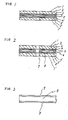
- Figure 1 shows, in a cross section, an optical disk according to one embodiment of the present invention
- 1 and 1′ are each a disk substrate made of a hard plastic such as methyl methacrylate or polycarbonate
- 2 and 2′ are each a recording surface
- 3 and 3′ are each a metallic reflective layer
- 4 and 4′ are each a reflective layer protecting layer which may be provided as required
- 5 is a smooth- surfaced silicone-made double-side pressure-sensitive adhesive member.
- Figure 2 shows, in a cross section, an optical disk according to another embodiment of the present invention
- 6 is an outer peripheral spacer made of the same material as that of substrate 1
- 7 is an inner peripheral spacer
- 8 is a hollow portion formed between the spacers 6 and 7.
- Figure 3 is a partial side view showing, in bulk form, a silicone-made pressure-sensitive adhesive member 5 comprising the above-described copolymer resin and diorganopolysiloxane.
- a film or sheet 9 having a very smooth (surface roughness: 1 ⁇ m or less) and low-adhesive surface is attached temporarily to both sides of the member 5.
- Materials of film or sheet 9 are a polyester, polypropylene, etc.
- the member 5 may be composed of a silicone-made pressure-sensitive adhesive alone, but if desired, a transparent plastic film such as a polyester, polyolefin, polyimide, polyether sulfone, polyether ether ketone or polyphenylene sulfite film may be used as the core material of the member 5.
- a transparent plastic film such as a polyester, polyolefin, polyimide, polyether sulfone, polyether ether ketone or polyphenylene sulfite film may be used as the core material of the member 5.
- the silicone-made pressure-sensitive adhesive which constitutes the member 5 is described below.
- the adhesive is comprised of a mixture or condensation product of a copolymer resin and a diorganopolysiloxane.
- the copolymer resin consists essentially of two components of a SiO2 unit and an R3SiO 0.5 unit such as trimethylsiloxane, triethylsiloxane, methylvinylpropylsiloxane, divinylmethylsiloxane, phenyldimethylsiloxane or diphenylsiloxane.
- the molar ratio of SiO2 to R3diO 0.5 unit is preferably in the range of from 1:0.3 to 1:1.2.
- the organic group in the triorganosiloxane represented by R3SiO 0.5 unit is constituted by an alkyl group having 1 to 4 carbon atoms such as methyl, ethyl or propyl, an alkenyl group such as vinyl or allyl, or an aryl group such as phenyl, naphthyl or tolyl.
- Diorganopolysiloxane consists essentially of an R2SiO unit such as dimethylsiloxane, diethylsiloxane, ethylmethylsiloxane, propylmethylsiloxane, or vinylmethylsiloxane and is a siloxane terminated with a hydroxyl group at the ends of its molecular chain.
- this diorganopolysiloxane should have a viscosity of at least 100,000 cSt, preferably 500,000 to 3,000,000 cSt, at 25°C. The viscosity is generally measured with, for example, Brookfield viscometer.
- the organic group in the siloxane represented by R2SiO unit is constituted by an alkyl group having 1 to 4 carbon atoms such as methyl, ethyl or propyl, an alkenyl group such as vinyl or allyl, or an aryl group such as phenyl or naphthyl. It is preferred that such an organic group contains at least 5 mol% of an aryl group, in particular a phenyl group.
- a preferred example of the diorganopolysiloxane is a siloxane rubber which contains both methyl and phenyl groups as organic groups, with the proportions of methyl phenyl groups being in the range of from 95 to 75 and from 5 to 25 mol%, preferably from 90 to 80 and from 10 to 20 mol%, respectively, from the standpoint that a shear adhesive strength of at least 10 kg/cm2 and a peeling strength of at least 1 kg/20 mm in a wet heat test under the conditions of 70°C x 85% R.H. for 2,000 hours can be securely obtained.
- the copolymer resin and diorganopolysiloxane are used with the weight ratio within the range of from 70:35 to 15:85, preferably from 60:40 to 25:75. They are mixed or condensed by a conventional method using an organic peroxide or a metal salt of, for example, carboxylic acid to prepare a silicone-made pressure-sensitive adhesive having excellent adhesive and cohesive properties under normal conditions (25 ⁇ 2°C; 65 ⁇ 5% R.H.). A filler, a plasticizer, a colorant or any other necessary additive may be incorporated into this adhesive, in suitable amounts.
- the pressure-sensitive adhesive thus prepared is applied on the surface of a base film or sheet having a very smooth (surface roughness: 1 ⁇ m or less) and low-adhesion surface to form a coating having a thickness of 10 to 300 ⁇ m and the resulting laminate is then wound on itself in roll form.
- the surface of the adhesive layer is covered with the same base film or sheet as described above to form a planar form. If a core material is interposed between the adhesive layers, the thickness of each adhesive layer is generally about 5 to 150 ⁇ m as a guide figure.
- the pressure-sensitive tape or sheet in either roll or planar form can be processed into a smooth-surface pressure-sensitive adhesive member by the following method: when the tape or sheet is in roll form, it is unwound and only the adhesive layer is cut to form a plurality of equally spaced circular adhesive members, with the undesired areas being then removed (in the case of producing an optical disk of the type as shown in Figure 1); when the tape or sheet is in planar form, only the adhesive layer is likewise cut to form concentric adhesive rings, one being of a larger diameter (for use as an outer peripheral spacer) than the other (for use as an inner peripheral spacer), and the base film or sheet under the center hole of the smaller-diameter ring is simultaneously punched out (in the case of producing an optical disk of the type as shown in Figure 2).
- the same method is applied to the planar tape or sheet and the base film or sheet under the adhesive layer may be peeled either before or after the processing.
- An optical disk is fabricated by the following procedures:
- the pressure-sensitive adhesive members spaced at equal distances on the surface of the base film or sheet are sequentially attached to the metallic reflective layer on one disk substrate, with care being taken to ensure that no air will be entrapped between the reflective layer and each adhesive member (this may be accomplished by pressing between rollers the base film or sheet having the adhesive members from one end portion), and after peeling off the base film or sheet, the other disk substrate is attached to the adhesive side of the first substrate.
- the thus fabricated optical disk of the present invention has the following advantages. Firstly, the pressure-sensitive adhesive member will not attack the substrates or any other parts of the disk. Secondly, the disk is free from any thermal strain since it does not require heating in the process of its fabrication. Thirdly, the disk is adapted for mass production. Fourthly, this optical disk retains high shear adhesive strength and peeling strength and will not generate any dropout noise even if it is subjected to a wet heat test under rigorous conditions.
- Two bulk substrates for optical disk were prepared from a polycarbonate resin by injection molding. A recording surface was formed one side of each bulk substrate. As a metallic reflective layer, an aluminum layer was formed in a thickness of about 1000 ⁇ over the recording surface by vacuum deposition to an optical disk substrate.
- a silicone pressure-sensitive adhesive consisting essentially of 50 parts of a copolymer resin comprising SiO2 and R3SiO 0.5 units in a molar ratio of 1:0.55 and 50 parts of diorganopolysiloxane (8000,000 cSt at 25°C) comprising R2SiO units containing 15 mol% phenyl group and 85 mol% methyl group was prepared.
- This adhesive was formed in a thickness of 30 ⁇ m on both sides of a 25 ⁇ m thick polyester film by conventional method.
- a polyester film which had been subjected to a release treatment to make the surface thereof smooth and low adhesive was bonded to both sides of the assembly to obtain an adhesive member in planar form.
- the adhesive member was punched to the same shapes as that of the disk substrates. After stripping the polyester film on one side thereof, the adhesive membrane was attached to the reflective layer on one substrate. Thereafter, the polyester film was stripped from the other side of the adhesive member and the adhesive membrane was attached to the reflective layer of the other substrate. The two substrates bonded through the adhesive membrane were pressed uniformly to obtain an optical disk.
- optical disk thus fabricated was entirely free from deformation and could be left to stand for 6 months without any corrosion occurring in the reflective layers.
- This optical disk was subjected to a wet heat test under the conditions of 70°C and 85% R.H. for 2,000 hours.
- the disk retained a shear adhesive strength of 15 kg/cm2 and a peeling strength of 1.1 kg/20 mm, and did not generate any dropout noise.
- An optical disk was obtained in the same manner as in Example 1 except that a diorganopolysiloxane wherein organic groups were all methyl groups was used.
- This optical disk was entirely free from deformation and corrosion. After a wet heat test, the disk retained a shear adhesive strength of 13 kg/cm2 and a peeling strength of 0.8 kg/20 mm.
- Shear adhesive strength and peeling strength were measured by the following methods.
- a 25 mm x 25 mm x 25 mm piece of an adhesive member was bonded to one end of a polycarbonate (PC) plate having a size of 1 mm thickness, 25 mm width and 125 mm length.
- PC polycarbonate
- One end of another PC plate having the same size was bonded to the other side of the adhesive member piece in such a manner that the two PC plates do not overlap.
- a 5 kg load was applied to the bonding portion of the PC plates for 15 min.
- the test piece was exposed to a 70°C x 85% R.H. atmosphere for 2,000 hours and thereafter left to stand at room temperature for more than 2 hours.
- the extremities of the PC plates were pulled in opposite directions at a speed of 200 mm/min.
- a 20 m wide piece of adhesive member having a polyester film coated on one side thereof was bonded to a PC plate having 1 mm thickness, 40 mm width and 125 mm length in such a manner that the uncoated other side of the piece faces down. Those were pressed by one reciprocal movement of a 2 kg rubber roll over the polyester film.
- the test piece was left to stand at room temperature for 30 minutes, exposed to a 70°C x 85% R.H. atmosphere for 2,000 hours, and then left to stand at room temperature for more than 2 hours.
- the cooled test piece was subjected to a 180° peeling test at a tensile speed of 300 mm/min.
Landscapes
- Adhesives Or Adhesive Processes (AREA)
- Optical Record Carriers And Manufacture Thereof (AREA)
- Laminated Bodies (AREA)
- Adhesive Tapes (AREA)
- Thermal Transfer Or Thermal Recording In General (AREA)
Applications Claiming Priority (2)
| Application Number | Priority Date | Filing Date | Title |
|---|---|---|---|
| JP43033/88 | 1988-02-24 | ||
| JP63043033A JP2656785B2 (ja) | 1988-02-24 | 1988-02-24 | 光デイスク |
Publications (2)
| Publication Number | Publication Date |
|---|---|
| EP0330197A2 true EP0330197A2 (de) | 1989-08-30 |
| EP0330197A3 EP0330197A3 (de) | 1991-09-04 |
Family
ID=12652618
Family Applications (1)
| Application Number | Title | Priority Date | Filing Date |
|---|---|---|---|
| EP19890103177 Withdrawn EP0330197A3 (de) | 1988-02-24 | 1989-02-23 | Optische Scheibe |
Country Status (4)
| Country | Link |
|---|---|
| US (1) | US4939011A (de) |
| EP (1) | EP0330197A3 (de) |
| JP (1) | JP2656785B2 (de) |
| KR (1) | KR890013618A (de) |
Cited By (9)
| Publication number | Priority date | Publication date | Assignee | Title |
|---|---|---|---|---|
| EP0410704A3 (en) * | 1989-07-28 | 1992-07-15 | Matsushita Electric Industrial Co., Ltd. | Optical recording apparatus |
| EP0419295A3 (en) * | 1989-09-22 | 1992-08-12 | Sharp Kabushiki Kaisha | Optical memory device |
| EP0844608A3 (de) * | 1996-11-20 | 1999-09-08 | Taiyo Yuden Co., Ltd. | Optisches Aufzeichnungsmedium |
| USRE36806E (en) * | 1994-07-29 | 2000-08-01 | 3M Innovative Properties Company | Internally damped rotatable storage article |
| EP1055233A1 (de) * | 1998-02-10 | 2000-11-29 | Minnesota Mining And Manufacturing Company | Verfahren zur herstellung eines optischen aufzeichnungsmediums |
| EP0797195A3 (de) * | 1996-03-21 | 2001-04-11 | Sony Corporation | Optische Platte und Plattenkassette |
| US6416838B1 (en) | 1999-10-28 | 2002-07-09 | 3M Innovative Properties Company | Compositions and articles made therefrom |
| US6599602B2 (en) | 1999-06-02 | 2003-07-29 | 3M Innovative Properties Company | Polycarbonate articles and adhesive composition therefor |
| US6830647B2 (en) * | 2000-06-29 | 2004-12-14 | Kitano Engineering Co., Ltd. | Method for laminating disc-shaped substrates |
Families Citing this family (22)
| Publication number | Priority date | Publication date | Assignee | Title |
|---|---|---|---|---|
| JPH02254648A (ja) * | 1989-03-28 | 1990-10-15 | Seiko Epson Corp | 光磁気ディスク |
| US5197049A (en) * | 1989-08-11 | 1993-03-23 | Apple Computer, Inc. | Head and media for optical data storage |
| DE69127398T2 (de) * | 1990-05-22 | 1998-01-02 | Canon Kk | Verfahren und Gerät zur Aufzeichnung und Wiedergabe von Informationen in Zellen, die eine vielfache Interferenz gebrauchen |
| US5146438A (en) * | 1990-05-30 | 1992-09-08 | E. I. Du Pont De Nemours & Co. | Method of making double-sided magneto-optical disks having reduced birefringence |
| US5244775A (en) * | 1991-03-20 | 1993-09-14 | Hitachi, Ltd. | Method of manufacturing an optical disc |
| US5951806A (en) * | 1995-11-30 | 1999-09-14 | Kitano Engineering Co., Ltd. | Method of manufacturing a storage disc |
| JPH09221651A (ja) * | 1996-02-16 | 1997-08-26 | Asahi Denka Kogyo Kk | エネルギー線反応性接着剤組成物 |
| DE59710799D1 (de) * | 1996-07-12 | 2003-11-06 | Ciba Sc Holding Ag | Speichermedien mit hoher Kapazität |
| US5932051A (en) * | 1996-09-05 | 1999-08-03 | Wea Manufacturing, Inc. | Pre-stressed bonding system for double sided compact discs |
| JP3014979B2 (ja) * | 1997-01-21 | 2000-02-28 | 日東電工株式会社 | 光ディスク製造方法およびそれに用いる装置 |
| JPH10208319A (ja) * | 1997-01-28 | 1998-08-07 | Kitano Eng Kk | ディスク基板の貼り合わせ方法 |
| GB2326014A (en) * | 1997-05-16 | 1998-12-09 | Jan Robert Coyle | A two-sided digital disc |
| US5932042A (en) * | 1997-06-19 | 1999-08-03 | Gensel; Lewis | Compact disc curing assembly line with deforming to a predetermined curvature prior to complete cure |
| US5786124A (en) * | 1997-06-25 | 1998-07-28 | Eastman Kodak Company | Optical recording elements containing metallized carbamoylazo dyes |
| US5821029A (en) * | 1997-06-25 | 1998-10-13 | Eastman Kodak Company | Optical recording elements containing mixtures of metallized carbamoylazo and cyanine dyes |
| KR20010014206A (ko) | 1997-06-26 | 2001-02-26 | 알프레드 엘. 미첼슨 | 광학 장치 및 이들의 배치 방법 |
| US6200402B1 (en) | 1998-01-27 | 2001-03-13 | Kitano Engineering Co., Ltd. | Method of and apparatus for laminating disc-shaped substrates |
| US6270943B1 (en) | 1998-02-20 | 2001-08-07 | Eastman Kodak Company | Optical recording elements comprising novel metallized azo ether dyes |
| US6582881B1 (en) | 1998-02-20 | 2003-06-24 | Eastman Kodak Company | Optical recording elements containing mixture of metallized azo ether and cyanine dyes |
| US6447981B1 (en) * | 1998-05-26 | 2002-09-10 | Eastman Kodak Company | Metallized azo thioether dyes |
| TW474034B (en) * | 2000-11-07 | 2002-01-21 | United Epitaxy Co Ltd | LED and the manufacturing method thereof |
| JP6576681B2 (ja) * | 2015-05-07 | 2019-09-18 | 日東電工株式会社 | 巻き芯保護用粘着シート、保護済巻き芯、およびフィルムの巻き取り巻き替え方法 |
Family Cites Families (9)
| Publication number | Priority date | Publication date | Assignee | Title |
|---|---|---|---|---|
| US4255316A (en) * | 1979-04-26 | 1981-03-10 | Dow Corning Corporation | Ceramifiable silicone adhesives |
| JPS593729A (ja) * | 1982-06-29 | 1984-01-10 | Konishiroku Photo Ind Co Ltd | 光学的情報記録媒体 |
| JPS60219098A (ja) * | 1984-04-16 | 1985-11-01 | Fuji Photo Film Co Ltd | レ−ザ−記録材料 |
| JPS6180532A (ja) * | 1984-09-28 | 1986-04-24 | Toshiba Corp | 光デイスク |
| US4572918A (en) * | 1984-10-26 | 1986-02-25 | Dow Corning Corporation | Foamable polyorganosiloxane compositions |
| US4518716A (en) * | 1984-10-26 | 1985-05-21 | Dow Corning Corporation | Foamable organosiloxane compositions |
| JPS61225253A (ja) * | 1985-03-29 | 1986-10-07 | Toray Silicone Co Ltd | 熱硬化性樹脂組成物 |
| JPS62148559A (ja) * | 1985-12-23 | 1987-07-02 | Mitsubishi Chem Ind Ltd | デイスク用ポリカ−ボネ−ト樹脂組成物 |
| US4753977A (en) * | 1986-12-10 | 1988-06-28 | General Electric Company | Water repellent for masonry |
-
1988
- 1988-02-24 JP JP63043033A patent/JP2656785B2/ja not_active Expired - Lifetime
-
1989
- 1989-02-23 EP EP19890103177 patent/EP0330197A3/de not_active Withdrawn
- 1989-02-24 US US07/315,098 patent/US4939011A/en not_active Expired - Fee Related
- 1989-02-24 KR KR1019890002162A patent/KR890013618A/ko not_active Withdrawn
Cited By (12)
| Publication number | Priority date | Publication date | Assignee | Title |
|---|---|---|---|---|
| EP0410704A3 (en) * | 1989-07-28 | 1992-07-15 | Matsushita Electric Industrial Co., Ltd. | Optical recording apparatus |
| EP0419295A3 (en) * | 1989-09-22 | 1992-08-12 | Sharp Kabushiki Kaisha | Optical memory device |
| USRE36806E (en) * | 1994-07-29 | 2000-08-01 | 3M Innovative Properties Company | Internally damped rotatable storage article |
| EP0797195A3 (de) * | 1996-03-21 | 2001-04-11 | Sony Corporation | Optische Platte und Plattenkassette |
| EP0844608A3 (de) * | 1996-11-20 | 1999-09-08 | Taiyo Yuden Co., Ltd. | Optisches Aufzeichnungsmedium |
| US6445676B1 (en) | 1996-11-20 | 2002-09-03 | Taiyo Yuden Co., Ltd. | Optical information medium |
| EP1055233A1 (de) * | 1998-02-10 | 2000-11-29 | Minnesota Mining And Manufacturing Company | Verfahren zur herstellung eines optischen aufzeichnungsmediums |
| US6168682B1 (en) | 1998-02-10 | 2001-01-02 | 3M Innovative Properties Company | Method of manufacturing an optical recording medium |
| US6599602B2 (en) | 1999-06-02 | 2003-07-29 | 3M Innovative Properties Company | Polycarbonate articles and adhesive composition therefor |
| US6815035B2 (en) | 1999-06-02 | 2004-11-09 | 3M Innovative Properties Company | Polycarbonate articles and adhesive composition therefor |
| US6416838B1 (en) | 1999-10-28 | 2002-07-09 | 3M Innovative Properties Company | Compositions and articles made therefrom |
| US6830647B2 (en) * | 2000-06-29 | 2004-12-14 | Kitano Engineering Co., Ltd. | Method for laminating disc-shaped substrates |
Also Published As
| Publication number | Publication date |
|---|---|
| JP2656785B2 (ja) | 1997-09-24 |
| KR890013618A (ko) | 1989-09-25 |
| US4939011A (en) | 1990-07-03 |
| JPH01217738A (ja) | 1989-08-31 |
| EP0330197A3 (de) | 1991-09-04 |
Similar Documents
| Publication | Publication Date | Title |
|---|---|---|
| US4939011A (en) | Optical disk | |
| US4906498A (en) | Flexible optical recording material in the shape of tape or floppy disk | |
| JPS62260838A (ja) | コ−チング用組成物、並びに下塗化製品およびその製法 | |
| JP3923044B2 (ja) | 巻回積層体 | |
| EP0067095B1 (de) | Verfahren zur Herstellung steifer optischer Scheiben | |
| JPH0443332B2 (de) | ||
| CA2088619A1 (en) | Adhesive Tape for Overcoating Splices in Polymer Coated Metal Tapes | |
| JPS61267947A (ja) | 光デイスク | |
| JPH11213467A (ja) | 貼り合わせ型光学式情報記録媒体の製造方法及び両面粘着性シート | |
| JPH05151625A (ja) | 光デイスクの製造方法 | |
| ES2010762A6 (es) | Cintas adhesivas sensibles a la presion de altas prestaciones y procedimiento para fabricarlas. | |
| JPS61182646A (ja) | 光デイスクとその製造法 | |
| JPH0428035A (ja) | 光ディスクの製造方法 | |
| KR100231104B1 (ko) | 자기기록 매체 | |
| JPH043347A (ja) | 光情報記録媒体 | |
| JP2002140842A (ja) | 光記録媒体の製造方法 | |
| JP2922631B2 (ja) | 光ディスク | |
| JPS6215912Y2 (de) | ||
| JP2972894B2 (ja) | 光情報記録媒体 | |
| JPS62229205A (ja) | 偏光フイルム保護用フイルム積層体 | |
| JPH0422289B2 (de) | ||
| JPS60115035A (ja) | 情報記録担体 | |
| JPS6032147A (ja) | 信号紀録ディスク | |
| JPS6387631A (ja) | 光学デイスクの製造方法 | |
| JPH0354745A (ja) | エアーサンドイッチ型両面記録光ディスク |
Legal Events
| Date | Code | Title | Description |
|---|---|---|---|
| PUAI | Public reference made under article 153(3) epc to a published international application that has entered the european phase |
Free format text: ORIGINAL CODE: 0009012 |
|
| AK | Designated contracting states |
Kind code of ref document: A2 Designated state(s): DE FR NL |
|
| PUAL | Search report despatched |
Free format text: ORIGINAL CODE: 0009013 |
|
| AK | Designated contracting states |
Kind code of ref document: A3 Designated state(s): DE FR NL |
|
| STAA | Information on the status of an ep patent application or granted ep patent |
Free format text: STATUS: THE APPLICATION IS DEEMED TO BE WITHDRAWN |
|
| 18D | Application deemed to be withdrawn |
Effective date: 19920305 |