EP0278480A2 - Verfahren zum Herstellen von Kohlenstoffschichten auf Plastikgegenständen durch chemische Gasphasenabscheidung im Mikrowellengebiet - Google Patents
Verfahren zum Herstellen von Kohlenstoffschichten auf Plastikgegenständen durch chemische Gasphasenabscheidung im Mikrowellengebiet Download PDFInfo
- Publication number
- EP0278480A2 EP0278480A2 EP88101879A EP88101879A EP0278480A2 EP 0278480 A2 EP0278480 A2 EP 0278480A2 EP 88101879 A EP88101879 A EP 88101879A EP 88101879 A EP88101879 A EP 88101879A EP 0278480 A2 EP0278480 A2 EP 0278480A2
- Authority
- EP
- European Patent Office
- Prior art keywords
- carbon
- film
- article
- microwave
- reaction chamber
- Prior art date
- Legal status (The legal status is an assumption and is not a legal conclusion. Google has not performed a legal analysis and makes no representation as to the accuracy of the status listed.)
- Granted
Links
Images


Classifications
-
- C—CHEMISTRY; METALLURGY
- C23—COATING METALLIC MATERIAL; COATING MATERIAL WITH METALLIC MATERIAL; CHEMICAL SURFACE TREATMENT; DIFFUSION TREATMENT OF METALLIC MATERIAL; COATING BY VACUUM EVAPORATION, BY SPUTTERING, BY ION IMPLANTATION OR BY CHEMICAL VAPOUR DEPOSITION, IN GENERAL; INHIBITING CORROSION OF METALLIC MATERIAL OR INCRUSTATION IN GENERAL
- C23C—COATING METALLIC MATERIAL; COATING MATERIAL WITH METALLIC MATERIAL; SURFACE TREATMENT OF METALLIC MATERIAL BY DIFFUSION INTO THE SURFACE, BY CHEMICAL CONVERSION OR SUBSTITUTION; COATING BY VACUUM EVAPORATION, BY SPUTTERING, BY ION IMPLANTATION OR BY CHEMICAL VAPOUR DEPOSITION, IN GENERAL
- C23C14/00—Coating by vacuum evaporation, by sputtering or by ion implantation of the coating forming material
- C23C14/22—Coating by vacuum evaporation, by sputtering or by ion implantation of the coating forming material characterised by the process of coating
- C23C14/24—Vacuum evaporation
-
- C—CHEMISTRY; METALLURGY
- C23—COATING METALLIC MATERIAL; COATING MATERIAL WITH METALLIC MATERIAL; CHEMICAL SURFACE TREATMENT; DIFFUSION TREATMENT OF METALLIC MATERIAL; COATING BY VACUUM EVAPORATION, BY SPUTTERING, BY ION IMPLANTATION OR BY CHEMICAL VAPOUR DEPOSITION, IN GENERAL; INHIBITING CORROSION OF METALLIC MATERIAL OR INCRUSTATION IN GENERAL
- C23C—COATING METALLIC MATERIAL; COATING MATERIAL WITH METALLIC MATERIAL; SURFACE TREATMENT OF METALLIC MATERIAL BY DIFFUSION INTO THE SURFACE, BY CHEMICAL CONVERSION OR SUBSTITUTION; COATING BY VACUUM EVAPORATION, BY SPUTTERING, BY ION IMPLANTATION OR BY CHEMICAL VAPOUR DEPOSITION, IN GENERAL
- C23C16/00—Chemical coating by decomposition of gaseous compounds, without leaving reaction products of surface material in the coating, i.e. chemical vapour deposition [CVD] processes
- C23C16/22—Chemical coating by decomposition of gaseous compounds, without leaving reaction products of surface material in the coating, i.e. chemical vapour deposition [CVD] processes characterised by the deposition of inorganic material, other than metallic material
- C23C16/26—Deposition of carbon only
-
- C—CHEMISTRY; METALLURGY
- C23—COATING METALLIC MATERIAL; COATING MATERIAL WITH METALLIC MATERIAL; CHEMICAL SURFACE TREATMENT; DIFFUSION TREATMENT OF METALLIC MATERIAL; COATING BY VACUUM EVAPORATION, BY SPUTTERING, BY ION IMPLANTATION OR BY CHEMICAL VAPOUR DEPOSITION, IN GENERAL; INHIBITING CORROSION OF METALLIC MATERIAL OR INCRUSTATION IN GENERAL
- C23C—COATING METALLIC MATERIAL; COATING MATERIAL WITH METALLIC MATERIAL; SURFACE TREATMENT OF METALLIC MATERIAL BY DIFFUSION INTO THE SURFACE, BY CHEMICAL CONVERSION OR SUBSTITUTION; COATING BY VACUUM EVAPORATION, BY SPUTTERING, BY ION IMPLANTATION OR BY CHEMICAL VAPOUR DEPOSITION, IN GENERAL
- C23C16/00—Chemical coating by decomposition of gaseous compounds, without leaving reaction products of surface material in the coating, i.e. chemical vapour deposition [CVD] processes
- C23C16/44—Chemical coating by decomposition of gaseous compounds, without leaving reaction products of surface material in the coating, i.e. chemical vapour deposition [CVD] processes characterised by the method of coating
- C23C16/50—Chemical coating by decomposition of gaseous compounds, without leaving reaction products of surface material in the coating, i.e. chemical vapour deposition [CVD] processes characterised by the method of coating using electric discharges
- C23C16/511—Chemical coating by decomposition of gaseous compounds, without leaving reaction products of surface material in the coating, i.e. chemical vapour deposition [CVD] processes characterised by the method of coating using electric discharges using microwave discharges
Definitions
- This invention relates to a microwave enhanced CVD method for coating plastic articles a with carbon film and its products.
- ECR CVD has attracted the interests of researchers as a new method of manufacturing thin films, particularly amorphous thin films.
- Matsuo et al discloses one type of such an ECR CVD apparatus in USP 4,401,054.
- This recent technique utilizes microwaves to energize a reactive gas into a plasma state by virtue of a magnetic field which functions to pinch the plasma gas within the excitation space. With this configuration, the reactive gas can absorb the energy of the microwave.
- a substrate to be coated is located distant from the excitation space (resonating space) for preventing the same from being spattered.
- the energized gas is showered on the substrate from the resonating space.
- the pressure is a resonating space is kept at 1 x 10 ⁇ 3 to 1 x 10 ⁇ 5 Torr at which electrons can be considered as independent particles and resonate with a microwave in an electron cyclotron resonance on a certain surface on which the magnetic field takes a particular strength required for ECR.
- the excited plasma is extrated from the resonating space, by means of a divergent magnetic field, to a deposition space which is located distant from the resonating space and in which is disposed a substrate to be coated.
- the carbon coating is implemented for several purposes.
- the carbon coating function to reinforce the strength of the components and endow the components with the resistance to abrasion.
- ornaments such as buttons, frames of spectacles and some parts of watches are coated, the carbon coatings become decorations.
- nitrogen and/or a nitrogen compound gas is inputted to the reaction chamber.
- the inputted nitrogen functions to prevent lattece defects from growing by virtue of external or internal stress.
- a boron compound is also inputted together with the nitrogen compound, the adhesivity of carbon deposited is improved.
- Boron nitride appear to be the binder between the carbon and the underlying substrate to be coated such as parts of watch.
- carbon and boron nitride are deposited on the substrate in the form of crystalline grain particles or a layer containing nitrogen and boron at less than 10%.
- a new CVD process has been culminated.
- the new process utilizes a mixed cyclotron resonance which was introduced firstly by the inventors.
- a sonic action of reactors gas itself must be taken into consideration as a non-negligible perturbation besides the interaction between respective particles of the reactive gas and magnetic field and microwave, and therefore charged particles of a reactive gas can be absorbed in a relatively wide resonating space.
- the pressure is maintained higher than 3 Torr.
- the mixed resonance the pressure in a reaction chamber is elevated 102-105 times as high as that of prior art.
- the mixed renonance can be established by increasing the pressure after ECR takes place at a low pressure.
- a plasma gas is placed in ECR condition at 1 x 10 ⁇ 3 to 1 x 10 ⁇ 5 Torr by inputting microwave under the existence of magnetic field.
- a reactive gas is inputted into the plasma gas so that the pressure is elevated to 0.1 to 300 Torr and the resonance is changed from ECR to MCR (Mixed Cyclotron Resonance).
- the MCR appears together with the whistler mode. Carbon can be decomposed and undergo a necessary reaction at only such a comparatively high pressure. In process, diamond is likely to grow selectively on convexies.
- the hardness of the diamond formed by the present invention is 1.3 to 3.0 times as high as that of diamond which has been made by prior art vapor phase method.
- film is used in a borad meaning. If a number of diamond particles are finely distributed on a surface, we call such a diamond coating as a “film.” Of course, a uniform and continuous amorphous layer is called a "film.”
- such parts When the parts of a wrist watch are coated with carbon film, such parts can be made of plastics and alminium or its alloy which have attractive processabilities so that the wrist watch is strongly formed and light weighted. Especially, electric field tends to be concentrated at the corners of the parts during process, and therefore such corners particularly exposed to external impacts when used can be coated with a carbon film thicker than that on a flat surface by a factor of two.
- the apparatus comprises a reaction chamber in which a plasma generating space 1 and an auxiliary space 2 are defined and which can be held at an appropriate pressure, a microwave generator 4, electro-magnets 5 and 5 ⁇ which are supplied with an electric power from a power supply 25, and a water cooling system 18.
- the plasma generating space 1 has a circular cross section.
- a hollow cylinder 10 ⁇ having inward-turned brims is rotatably supported in the space so that a microwave emitted from the microwave generator 4 passes through the cylinder along its axis.
- the cylinder 10 ⁇ is made of stainless steel or a quartz and turned by means of a motor 16 through a gear.
- a evacuating system comprising a turbo molecular pump 8 and a rotary pump 14 which are connected with the reaction chamber through pressure controlling valves 11, 12 and 13. The process with this apparatus is carried out as follows.
- Objects 10 to be coated with carbon film are plastics such as gear-wheels with 3-10 mm in diameter and 0.2-2.0 mm in thickness, screws, buttons, toy parts which need sufficient hardnesses, frames of spectacles, the entire external surface of ball pens, propelling pencils and the like, or other ornaments having various, external shapes which are to be coated with diamond, or parts of watchs such as frames made of plastics, windows made of glasses or plastics.
- the objects 10 are put in the cylinder 10 ⁇ which is to turn at 0.1-10 rpm during process. At the same time, the objects 10 are heated to a certain elevated temperature at which the objects are not damaged.
- the elevated temperature is, e.g., 150-300°C; for aluminium or its alloy objects, e.g., 400-700°C; for iron, stainless steel or other metallic objects, e.g., 700-1000°C.
- the cylinder 10 ⁇ although the means is not illustrated in the figure, is shaken by micro-vibration of 100Hz-10KHz. By the turning and the vibration, the surfaces of the objects exposed to the reactive gas are always switching during process.
- the reaction chamber is evacuated by the turbo molecular pump 8 and the rotary pump to 1 x 10 ⁇ 6 Torr or lower.
- argon, helium or hydrogen as a non-productive gas is introduced to the reaction chamber from a gas introducing system 6 at 30SCCM, and a microwave of 2.45 GHz is emitted from the microwave generator at 500m W through a microwave introduction window 15 to the plasma generating space 1 which is subjected to an magnetic field of about 2 K Gauss induced by the magnets 5 and 5 ⁇ .
- the pressure of the non-productive gas is 1 x 10 ⁇ 4 Torr.
- a plasma is generated in the space 1 at a high density by the energy of the microwave.
- the surfaces of the objects 10 is cleaned by high energy electrons and non-productive atoms.
- C2H2, C2H4 and/or CH4 are introduced at 200 SCCM through a introduction system 7.
- a large amount of hydrogen is introduced into the reaction chamber so that the carbon compound gas is diluted with the hydrogen to 0.1-2.0 %.
- the pressure of the reaction chamber is maintained at 0.1-300 Torr, preferably 3-30 Torr, e.g., 10 Torr.
- the product can be deposited at a high speed and spread over widely in the chamber.
- the reactive gas is excited by the energy of microwave in the same manner as carried out with the non-productive gas explained in the foregoing description.
- carbon is deposited in the form of a diamond film or an i-carbon (insulation carbon consisting of crystalline particles) film on the objects 10.
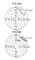
- Fig.2(A) is a graphical diagram showing the distribution of magnetic field on the region 30 in Fig.1 Curves on the diagram are plotted along equipotential surfaces and given numerals indicating the strengths on the respective curves of the magnetic field induced by the magnets 5 and 5 ⁇ having a power of 2000 Gauss.
- the strength of the magnetic field can be controlled so that the magnetic field becomes largely uniform over the surface to be coated which is located in the region 100 where the magnetic field (875 ⁇ 185 Gauss) and the electric field interact.
- a reference 26 designates the equipotential surface of 875 Gauss at which ECR (electron cyclotron resonance) condition between the magnetic field and the frequency of the microwave is sutisfied.
- ECR electron cyclotron resonance
- MCR mixed cyclotron resonance
- Fig.2(B) is a graphical diagram of which the X-axis corresponds to that of Fig.2(A) and shows the strength of electric field of the microwave in the plasma generating space 1. The strength of the electric field takes its maximum value in the regions 100 and 100 ⁇ .
- a uniform film can be formed on a cirlcular substrate having a diameter of up to 100mm.
- a film is formed in the chamber on a circular substrate having a diameter of up to 50 mm with a uniform thickness and a uniform quality.
- the diameter of the space 1 can be sized double with respect to the vertical direction of Fig.2(A) by making use of 1.225 GHz as the frequency of the microwave.
- Figs.3(A) and 3(B) are graphical diagrams showing the distributions of the magnetic field and the electric field due to microwave emitted from the microwave generator 4 on a cross section of the plasma generating space 1. The curves in the circles of the figures are plotted along equipotential surfaces and given numerals showing the strength. As shown in Fig.3(B), the electric field reaches its maximum value at 25 KV/m.
- the pressure in the reaction chamber is chosen at that required for ECR condition, so that a preliminary plasma discharge takes place. While the discharge continues, the pressure is changed to 1 Torr to 3 x 10³ Torr where a mixed resonance takes place with a plasma of which particles have a mean free path of 0.05 mm to several milimeters, normally not more than 1 mm.
- a number of objects 10 such as plastic gear components are placed in the cylinder 10 ⁇ , and the reaction chamber is evacuated to 1 x 10 ⁇ 6 Torr or a higher vacuum condition. Then, hydrogen gas is introduced from a gas introducing system 6 at 30 SCCM, and a microwave of 500 Watt at 2.45 GHz is emitted from the microwave generator 4 thorugh a microwave introduction window 15 to the plasma generating space 1 which is subjected to an magnetic field of about 2 K Gauss induced by the magnets 5 and 5 ⁇ . The hydrogen is excited into a high density plasma state in the space 1 at 1 x 10 ⁇ 4 Torr by the energy of the microwave. The surfaces of the objects 10 are cleaned by high energy electrons and hydrogen atoms.
- a carbon compound gas as the productive gas such as C2H2, C2H4, CH3OH, C2H5OH or CH4 are inputted at 30 SCCM through an introduction system 7.
- the productive gas is diluted with hydrogen at a sufficiently thin density, e.g., 0.1 to 5 %.
- a nitrogen or its compound gas such as ammonia or nitrogen gas, is inputted to the reaction chamber from the introduction system.
- the proportion of the nitrogen compound gas to the carbon compound gas is 0.1%-5%.
- the pressure in the reaction chamber is maintained at 0.1 Torr-300 Torr, preferably 3-30 Torr, e.g., 1 Torr.
- a objects 10 are disposed in the cylinder 10 ⁇ , and the reaction chamber is evacuated to 1 x 10 ⁇ 6 Torr of a higher vacuum condition. Then, hydrogen gas is introduced from a gas introducing system 6 at 300 SCCM, and a microwave of 1 Kilo Watt at 2.45 GHz is emitted from the microwave generator 4 thorugh a microwave introduction window 15 to the plasma generating space 1 which is subjected to an magnetic field of about 2 K Gauss inducing by the magnets 5 and 5 ⁇ . The hydrogen is excited into a high density plasma state in the space 1 by the energy of the microwave. The surfaces of the objects 10 are cleaned by high energy electrons and hydrogen atoms.
- a cabon compound gas as the productive gas such as C2H2, C2H4, CH3OH, C2H5OH or CH4 are inputted at 3 SCCM through an introduction system 7.
- the productive gas is diluted with hydrogen at a sufficiently thin density, e.g., 0.1 to 15 %.
- the proportion of B2H6(BF3)+NH3 to the carbon compuond gas is 1%-50%.
- the pressure in the reaction chamber is maintained at 1 Torr-760 Torr, preferably higher than 10 Torr or 10-100 Torr, e.g., 30 Torr.
- 10 Torr or 10-100 Torr e.g., 30 Torr.
- the objects 10 disposed in the cylinder 10 ⁇ are coated with carbon containing nitrogen and boron (or in the form of boron nitride).
- the product includes carbon and boron nitride as the main components, the sum of whose proportions is at least 90%.
- the film is made of the mixture of boron nitride and diamond. As the microwave power is increased from 1KW to 5KW, the proportion of diamond in the film increases.
- the plasma gas becomes containing fluorine and which fluorine functions to eliminate impurity residing on the surface to be coated by etching.
- a film formation process was performed in the same manner as in the above but without using a magnetic field. As a result, a graphite film was deposited.
- amorphous or microcrystalline film can also be deposited by appropriately selecting the deposition condition.
- An amorphous film is deposited when carbon compound gas is diluted with the larger amount of hydrogen gas, when the input power is comparatively small and when the process temperature is comparatively low.
- the carbon formed in accordance with the invention has a very high hardness irrespective of whether the carbon is amorphous or crystalline.
- the Vickers hardness is 4500-6400 Kg/mm2, e.g., 2000 Kg/mm2.
- the thermal conductivity is not lower than 2.5 W/cm deg, e.g., 5.0-6.6 W/cm deg.
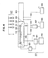
- Fig.4 is a cross sectional view showing a CVD apparatus for deposition by virtue of an r.f. power.
- the apparatus comprises a reaction chamber 101, a loading chamber 103, a rotary pump 105 for evacuating the loading chamber 103, a turbo molecular pump 107 associated with a rotary pump 109 for evacuating both the reaction chamber 101 and the loading chamber 103, a gas feeding system 127 for inputting process gas such as reactive gas or dopant gas through a nozzle 129, a sub strate holder 111 for supporting objects 113, electrodes 115 disposed opposite to the holder 111, an RF power supply 117 consisting of a radiofrequency power source 119 associated with a matching circuit 121 and a DC bias circuit 123 for supply an r.f. power between the electrodes 115 and the substrate holder 111, and a
- a reactive gas composed of a gaseous carbon compound such as CH4, C2H4 and C2H2, and a dopant gas such as nitrogen, a nitrogen compound gas and a boron compound gas if necessary were inputted to the reaction chamber at 1 x 10 ⁇ 3 to 5 x 10 ⁇ 1 Torr.
- the carbon compound gas was diluted with hydrogen at 50 mol%.
- the objects 113 were heated to not higher than 450°C by means of the heater 125. In this condition, a vapor reaction was initiated by means of r.f. power inputted from the power supply 117. The r.f.
- a photosensitive printing drum is formed by means of plasma CVD suitable for carbon film deposition.
- the photosensitive material forming photo-detecting layer is organic photoconductor(OPC) which suffers from a high temperature higher than 200°C.
- organic conductors are poly-N-vinyl-caryazole(PVC), tri-nitro-fluorlenone (TNF) and so forth.
- PVC poly-N-vinyl-caryazole
- TNF tri-nitro-fluorlenone
- the OPC layer is coated with an organic insulating film such as polyethylene, polycarbonate, polyurethane, barilene and so forth.
- the organic insulating film in turn is coated with a carbon film according to the invention which has a hardness and a surface smoothness, and can be formed adhesively at a relative low temperature.
- a carbon film according to the invention which has a hardness and a surface smoothness, and can be formed adhesively at a relative low temperature.
- Between the OPC film and the underlying metallic substrate may be disposed a p or n type silicone semiconductor layer, if necessary.
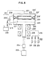
- a stainless steel container 201 is provided with a lid 201 ⁇ and forms a reaction space therein.
- a substrate 210 in the form of a cylinder made of Al, Cr, Mo, Au, Ir, Nr, V, Ti, Pd and Pt is disposed in the space.
- the substrate 210 has been coated with a resin barrier film on the external surface.
- a pair of holders 208 and 208 ⁇ is provided on the opposed side wall of the container 201 to support and rotate the substrate 201 around its axis.
- On the lid 1 ⁇ is provided a homogenizer of a meshed electrode 220 ⁇ through which exhausted gas is removed by an exhaustion system 11 comprising a pump 209 and valves 214 and 215.
- a resonating space 202 Opposite to the lid 1 ⁇ , formed is a resonating space 202 which is subjected to the magnetic field induced by an electromagnet 205 and 205 ⁇ .
- a microwave oscillator 203 is connected with the opposed end of the resonating space 202 with an associated matching apparatus 204.
- the power source is a high frequency power supply 206 including a DC power source connected between the holders 208 and 208 ⁇ and the meshed electrode 220 which functions as a homogenizer.
- the power inputted to the reaction space is for example an electric field induced by 13.56 MHz voltage biassed by a DC voltage applied between the holders and the meshed electrode.
- the substrate surface is oriented perpenducular to the electric field in the figure.
- the container 201 may be provided with a means for shuttling the substrate in the axial direction during the axial rotation if the substrate is somewhat long. Also a plurality of substrates may be treated at once by providing a plurality of pairs of holders arranged in the normal direction to the drawing sheet. The homogenizer helps the reactive gas to spread over a wide area in the reaction space.
- a reactive gas consisting of methane and diborane or phosphine (as a dopant) diluted with hydrogen is inputted to the reaction space through the introduction system 213.
- the abandance of hydrogen in a produced carbon is increased and the optical energy gap is 2.5 to 3.5 eV.
- a possitive potential is given to the holders relative to the electrode 220, hydrogen ions are repulsed and therefore the energy gap decreases resulting in a band gas of 1.0 to 2.0 eV.
- the substrate temperature is chosen between -100 to +200°C, preferably -100 to +150°C, so that no damage appears to the underlying resin layer whose thermal resistivity is not so high.
- the deposition speed when the reactive gas is pre-excited in advance of entering the reaction space, the deposition speed is 500 to 1000 ⁇ /min. In absence of the pre-excitation, the deposition speed reamins as low as 100 to 200 ⁇ /min.
- the thichness of the carbon film on the substrate is 0.1 to 4 micron, preferbly 0.5 to 2 micron with the wider energy gap, and eventually a barrier layer having good abrasion-proof characteristic is obtained.
- the Vickers hardness of the carbon coating formed in accordance with the embodiment is not lower than 2000Kg/mm2 and the thermal conductivity is not lower than 2.5W/cm deg, whereby the life time of the copying machine employing the coating is improved so that copying is possible more than two hundreds thousands times over without wear of the drum.
- the reaction pressure was 0.1 Torr. Hydrogen and methane were introduced respectively at 200SCCM. Microwave was inputted to the resonating space at 2.45 GHz and at 30 W to 1.3 KW, eg., 500 W. The strength of magnetic field in the resonating space was 875 Gauss. The electric power was inputted to the reaction space at 13.56 MHz and at 500 W. Although the substrate was not heated intentionally, the temperature was elevated to 150°C in light of plasma.
- the deposition speed of amorphous carbon was 30 ⁇ /sec during the deposition time of 15 minutes.
- the speed was 20 times higher than that obtained by plasma CVD, i.e. 1.5 ⁇ /sec.
- the amorphous carbon film was 2300Kg/mm2 in Vickers hardness, 1010 ohm cm in resistivity and 1.8 eV in optical energy gap.
- a carbon film was deposited on the surface of a photosensitive drum made of aluminium coated with an OPC film with 25 cm in diameter and 30 cm in length, in the same way as the first experiment except the specified in what follow.
- the electric power was inputted to the reaction space at 300 W biassed by +200 V.
- the pressure in the reaction space was 0.3 Torr.
- a 0.4 micron thick carbon film was deposited at 200 ⁇ /min.
- the substrate was shuttled in the axial direction and cooled to -30°C during process.
- the DC bias is +400V. As a result, a 0.5 micron thick carbon film was formed.
- a super lattice structure can be also formed.
- a boron nitride (BN) thin film is deposited in the same way as illustrated in the above but without using carbon compound gas.
- a carbon thin film and a BN thin film are deposited in turn many times so that a super lattice structure is sttacked on a substrate.
Applications Claiming Priority (2)
| Application Number | Priority Date | Filing Date | Title |
|---|---|---|---|
| JP62028957A JPH0676666B2 (ja) | 1987-02-10 | 1987-02-10 | 炭素膜作製方法 |
| JP28957/87 | 1987-02-10 |
Publications (4)
| Publication Number | Publication Date |
|---|---|
| EP0278480A2 true EP0278480A2 (de) | 1988-08-17 |
| EP0278480A3 EP0278480A3 (en) | 1989-02-22 |
| EP0278480B1 EP0278480B1 (de) | 1993-10-06 |
| EP0278480B2 EP0278480B2 (de) | 1996-01-31 |
Family
ID=12262896
Family Applications (1)
| Application Number | Title | Priority Date | Filing Date |
|---|---|---|---|
| EP88101879A Expired - Lifetime EP0278480B2 (de) | 1987-02-10 | 1988-02-09 | Verfahren zum Herstellen von Kohlenstoffschichten auf Plastikgegenständen durch chemische Gasphasenabscheidung im Mikrowellengebiet |
Country Status (6)
| Country | Link |
|---|---|
| US (1) | US5601883A (de) |
| EP (1) | EP0278480B2 (de) |
| JP (1) | JPH0676666B2 (de) |
| KR (1) | KR930003605B1 (de) |
| CN (1) | CN1023329C (de) |
| DE (1) | DE3884636T2 (de) |
Cited By (7)
| Publication number | Priority date | Publication date | Assignee | Title |
|---|---|---|---|---|
| EP0334109A1 (de) * | 1988-03-24 | 1989-09-27 | Siemens Aktiengesellschaft | Verfahren und Vorrichtung zum Herstellen von aus amorphen Silizium-Germanium-Legierungen bestehenden Halbleiterschichten nach der Glimmentladungstechnik, insbesondere für Solarzellen |
| EP0361206A1 (de) * | 1988-09-13 | 1990-04-04 | Semiconductor Energy Laboratory Co., Ltd. | Mit einem keramischen Film überzogener Gegenstand |
| DE4023511A1 (de) * | 1989-07-24 | 1991-01-31 | Tdk Corp | Verfahren und vorrichtung zur durchfuehrung einer vakuumbehandlung |
| GB2248636A (en) * | 1990-10-13 | 1992-04-15 | British Petroleum Co Plc | A process for depositing a carbon coating on a fibre using a haloalkyne |
| EP0304220B1 (de) * | 1987-08-10 | 1994-12-07 | Semiconductor Energy Laboratory Co., Ltd. | Dünnfilmkohlewerkstoff und Verfahren zum Aufbringen |
| GB2287473A (en) * | 1994-03-15 | 1995-09-20 | Dr Joseph Franks | Diamond coated polymer devices for biomedical applications |
| EP2009170A1 (de) * | 2007-06-25 | 2008-12-31 | Electrolux Home Products Corporation N.V. | Beschichtete Waschmittelschublade |
Families Citing this family (17)
| Publication number | Priority date | Publication date | Assignee | Title |
|---|---|---|---|---|
| JPH0853116A (ja) * | 1994-08-11 | 1996-02-27 | Kirin Brewery Co Ltd | 炭素膜コーティングプラスチック容器 |
| JP2737720B2 (ja) * | 1995-10-12 | 1998-04-08 | 日本電気株式会社 | 薄膜形成方法及び装置 |
| CN1062541C (zh) * | 1996-01-30 | 2001-02-28 | 中国科学院山西煤炭化学研究所 | 一种碳/氮化硼复合材料及其制备方法 |
| DE19635736C2 (de) * | 1996-09-03 | 2002-03-07 | Saxonia Umformtechnik Gmbh | Diamantähnliche Beschichtung |
| JP3469761B2 (ja) * | 1997-10-30 | 2003-11-25 | 東京エレクトロン株式会社 | 半導体デバイスの製造方法 |
| US6795636B1 (en) | 2000-03-05 | 2004-09-21 | 3M Innovative Properties Company | Radiation-transmissive films on glass articles |
| US6749813B1 (en) | 2000-03-05 | 2004-06-15 | 3M Innovative Properties Company | Fluid handling devices with diamond-like films |
| JP2002074652A (ja) * | 2000-08-24 | 2002-03-15 | Fuji Electric Co Ltd | 記録媒体の製造方法 |
| US6869645B2 (en) * | 2001-10-23 | 2005-03-22 | Acushnet Company | Method for plasma treatment of golf balls |
| US6541397B1 (en) * | 2002-03-29 | 2003-04-01 | Applied Materials, Inc. | Removable amorphous carbon CMP stop |
| DE10227836B4 (de) * | 2002-06-21 | 2006-02-09 | Mikrowellen-Systeme Mws Gmbh | Verfahren, Verwendung des Verfahrens sowie Verwendung eines Mikrowellenheizgeräts zum Mischen und zur Auslösung von chemischen Reaktionen von Feststoffgemischen oder Suspensionen in einem Mikrowellenfeld |
| DE10331608A1 (de) * | 2003-07-12 | 2005-01-27 | Hew-Kabel/Cdt Gmbh & Co. Kg | Verfahren zum Beschichten und/oder partiellen Umspritzen von flexiblem langgestrecktem Gut |
| JP2008014782A (ja) * | 2006-07-05 | 2008-01-24 | Seiko Epson Corp | 時計用歯車部品および時計 |
| FR2921388B1 (fr) * | 2007-09-20 | 2010-11-26 | Air Liquide | Dispositif et procede de depot cvd assiste par plasma tres haute frequence a la pression atmospherique, et ses applications |
| US20100174245A1 (en) * | 2009-01-08 | 2010-07-08 | Ward Dean Halverson | System for pretreating the lumen of a catheter |
| JP5446770B2 (ja) | 2009-11-20 | 2014-03-19 | 株式会社リコー | 電圧検出回路 |
| FR2975404B1 (fr) * | 2011-05-19 | 2014-01-24 | Hydromecanique & Frottement | Piece avec revetement dlc et procede d'application du revetement dlc |
Citations (4)
| Publication number | Priority date | Publication date | Assignee | Title |
|---|---|---|---|---|
| FR2514743A1 (fr) * | 1981-10-21 | 1983-04-22 | Rca Corp | Pellicule amorphe a base de carbone, du type diamant, et son procede de fabrication |
| DE3316693A1 (de) * | 1983-05-06 | 1984-11-08 | Leybold-Heraeus GmbH, 5000 Köln | Verfahren zum herstellen von amorphen kohlenstoffschichten auf substraten und durch das verfahren beschichtete substrate |
| EP0157212A2 (de) * | 1984-04-02 | 1985-10-09 | American Cyanamid Company | Mit einem haftfesten diamantähnlichen Film überzogener Gegenstand |
| EP0175980A2 (de) * | 1984-09-10 | 1986-04-02 | Ovonic Synthetic Materials Company, Inc. | Glimmentladung Verfahren zur Herstellung eines Kohlstoffüberzuges auf einem Substrat und die so hergestellten Überzüge |
Family Cites Families (29)
| Publication number | Priority date | Publication date | Assignee | Title |
|---|---|---|---|---|
| US2721154A (en) * | 1949-06-24 | 1955-10-18 | Ward Blenkinsop & Co Ltd | Production of conducting layers upon electrical insulating materials |
| US4104441A (en) * | 1975-07-29 | 1978-08-01 | Institut Sverkhtverdykh Materialov Ssr | Polycrystalline diamond member and method of preparing same |
| US4060660A (en) * | 1976-01-15 | 1977-11-29 | Rca Corporation | Deposition of transparent amorphous carbon films |
| US4504519A (en) * | 1981-10-21 | 1985-03-12 | Rca Corporation | Diamond-like film and process for producing same |
| US4434188A (en) * | 1981-12-17 | 1984-02-28 | National Institute For Researches In Inorganic Materials | Method for synthesizing diamond |
| US4737379A (en) * | 1982-09-24 | 1988-04-12 | Energy Conversion Devices, Inc. | Plasma deposited coatings, and low temperature plasma method of making same |
| US4701317A (en) * | 1983-06-14 | 1987-10-20 | Director-General Of Agency Of Industrial Science And Technology | Highly electroconductive films and process for preparing same |
| US4524106A (en) * | 1983-06-23 | 1985-06-18 | Energy Conversion Devices, Inc. | Decorative carbon coating and method |
| JPS6033300A (ja) * | 1983-08-04 | 1985-02-20 | Nec Corp | ダイヤモンドの気相合成方法及びその装置 |
| US4599135A (en) * | 1983-09-30 | 1986-07-08 | Hitachi, Ltd. | Thin film deposition |
| CA1232228A (en) * | 1984-03-13 | 1988-02-02 | Tatsuro Miyasato | Coating film and method and apparatus for producing the same |
| JPS60195092A (ja) * | 1984-03-15 | 1985-10-03 | Tdk Corp | カ−ボン系薄膜の製造方法および装置 |
| US4582727A (en) * | 1984-03-20 | 1986-04-15 | Amax Inc. | Varnish-bonded, carbon-coated metal products |
| DE3421739A1 (de) * | 1984-06-12 | 1985-12-12 | Battelle-Institut E.V., 6000 Frankfurt | Verfahren zur herstellung von diamantartigen kohlenstoffschichten |
| SE442305B (sv) * | 1984-06-27 | 1985-12-16 | Santrade Ltd | Forfarande for kemisk gasutfellning (cvd) for framstellning av en diamantbelagd sammansatt kropp samt anvendning av kroppen |
| US4770940A (en) * | 1984-09-10 | 1988-09-13 | Ovonic Synthetic Materials Company | Glow discharge method of applying a carbon coating onto a substrate and coating applied thereby |
| JPS61121859A (ja) * | 1984-11-15 | 1986-06-09 | Showa Denko Kk | 気相法ダイヤモンド合成に使用する基板処理法 |
| US4645713A (en) * | 1985-01-25 | 1987-02-24 | Agency Of Industrial Science & Technology | Method for forming conductive graphite film and film formed thereby |
| JPH0697660B2 (ja) * | 1985-03-23 | 1994-11-30 | 日本電信電話株式会社 | 薄膜形成方法 |
| US4725345A (en) * | 1985-04-22 | 1988-02-16 | Kabushiki Kaisha Kenwood | Method for forming a hard carbon thin film on article and applications thereof |
| US4603082A (en) * | 1985-04-29 | 1986-07-29 | Rca Corporation | Diamond-like film |
| JPS62123096A (ja) * | 1985-11-21 | 1987-06-04 | Showa Denko Kk | ダイヤモンドの合成法 |
| CH664377A5 (de) * | 1986-01-16 | 1988-02-29 | Balzers Hochvakuum | Dekorative schwarze verschleissschutzschicht. |
| US4715937A (en) * | 1986-05-05 | 1987-12-29 | The Board Of Trustees Of The Leland Stanford Junior University | Low-temperature direct nitridation of silicon in nitrogen plasma generated by microwave discharge |
| US4777090A (en) * | 1986-11-03 | 1988-10-11 | Ovonic Synthetic Materials Company | Coated article and method of manufacturing the article |
| JPS63121667A (ja) * | 1986-11-10 | 1988-05-25 | Semiconductor Energy Lab Co Ltd | 薄膜形成装置 |
| JPS63145782A (ja) * | 1986-12-08 | 1988-06-17 | Semiconductor Energy Lab Co Ltd | 薄膜形成方法 |
| KR900008505B1 (ko) * | 1987-02-24 | 1990-11-24 | 세미콘덕터 에너지 라보라터리 캄파니 리미티드 | 탄소 석출을 위한 마이크로파 강화 cvd 방법 |
| US4809876A (en) * | 1987-08-27 | 1989-03-07 | Aluminum Company Of America | Container body having improved gas barrier properties |
-
1987
- 1987-02-10 JP JP62028957A patent/JPH0676666B2/ja not_active Expired - Fee Related
-
1988
- 1988-02-09 EP EP88101879A patent/EP0278480B2/de not_active Expired - Lifetime
- 1988-02-09 DE DE88101879T patent/DE3884636T2/de not_active Expired - Fee Related
- 1988-02-10 KR KR1019880001320A patent/KR930003605B1/ko not_active IP Right Cessation
- 1988-02-10 CN CN88100841A patent/CN1023329C/zh not_active Expired - Lifetime
-
1994
- 1994-09-28 US US08/314,456 patent/US5601883A/en not_active Expired - Fee Related
Patent Citations (4)
| Publication number | Priority date | Publication date | Assignee | Title |
|---|---|---|---|---|
| FR2514743A1 (fr) * | 1981-10-21 | 1983-04-22 | Rca Corp | Pellicule amorphe a base de carbone, du type diamant, et son procede de fabrication |
| DE3316693A1 (de) * | 1983-05-06 | 1984-11-08 | Leybold-Heraeus GmbH, 5000 Köln | Verfahren zum herstellen von amorphen kohlenstoffschichten auf substraten und durch das verfahren beschichtete substrate |
| EP0157212A2 (de) * | 1984-04-02 | 1985-10-09 | American Cyanamid Company | Mit einem haftfesten diamantähnlichen Film überzogener Gegenstand |
| EP0175980A2 (de) * | 1984-09-10 | 1986-04-02 | Ovonic Synthetic Materials Company, Inc. | Glimmentladung Verfahren zur Herstellung eines Kohlstoffüberzuges auf einem Substrat und die so hergestellten Überzüge |
Non-Patent Citations (1)
| Title |
|---|
| THIN SOLID FILMS, vol. 128, no. 3/4, June 1985, pages 341-351, Elsevier Sequoia, Lausanne, CH; O. MATSUMOTO et al.: "Effect of dilution gases in methane on the deposition of diamond-like carbon in a microwave discharge" * |
Cited By (10)
| Publication number | Priority date | Publication date | Assignee | Title |
|---|---|---|---|---|
| EP0304220B1 (de) * | 1987-08-10 | 1994-12-07 | Semiconductor Energy Laboratory Co., Ltd. | Dünnfilmkohlewerkstoff und Verfahren zum Aufbringen |
| EP0334109A1 (de) * | 1988-03-24 | 1989-09-27 | Siemens Aktiengesellschaft | Verfahren und Vorrichtung zum Herstellen von aus amorphen Silizium-Germanium-Legierungen bestehenden Halbleiterschichten nach der Glimmentladungstechnik, insbesondere für Solarzellen |
| EP0361206A1 (de) * | 1988-09-13 | 1990-04-04 | Semiconductor Energy Laboratory Co., Ltd. | Mit einem keramischen Film überzogener Gegenstand |
| DE4023511A1 (de) * | 1989-07-24 | 1991-01-31 | Tdk Corp | Verfahren und vorrichtung zur durchfuehrung einer vakuumbehandlung |
| US5082685A (en) * | 1989-07-24 | 1992-01-21 | Tdk Corporation | Method of conducting plasma treatment |
| GB2248636A (en) * | 1990-10-13 | 1992-04-15 | British Petroleum Co Plc | A process for depositing a carbon coating on a fibre using a haloalkyne |
| GB2287473A (en) * | 1994-03-15 | 1995-09-20 | Dr Joseph Franks | Diamond coated polymer devices for biomedical applications |
| GB2287473B (en) * | 1994-03-15 | 1998-01-07 | Dr Joseph Franks | Coated polymer devices for biomedical applications |
| EP2009170A1 (de) * | 2007-06-25 | 2008-12-31 | Electrolux Home Products Corporation N.V. | Beschichtete Waschmittelschublade |
| RU2487204C2 (ru) * | 2007-06-25 | 2013-07-10 | Электролюкс Хоум Продактс Корпорейшн Н.В. | Ящик с покрытием для моющего средства |
Also Published As
| Publication number | Publication date |
|---|---|
| KR930003605B1 (ko) | 1993-05-08 |
| JPS63195267A (ja) | 1988-08-12 |
| EP0278480B1 (de) | 1993-10-06 |
| US5601883A (en) | 1997-02-11 |
| KR880010151A (ko) | 1988-10-07 |
| CN1023329C (zh) | 1993-12-29 |
| DE3884636T2 (de) | 1994-01-27 |
| EP0278480A3 (en) | 1989-02-22 |
| EP0278480B2 (de) | 1996-01-31 |
| DE3884636D1 (de) | 1993-11-11 |
| CN88100841A (zh) | 1988-10-05 |
| JPH0676666B2 (ja) | 1994-09-28 |
Similar Documents
| Publication | Publication Date | Title |
|---|---|---|
| EP0278480A2 (de) | Verfahren zum Herstellen von Kohlenstoffschichten auf Plastikgegenständen durch chemische Gasphasenabscheidung im Mikrowellengebiet | |
| US5013579A (en) | Microwave enhanced CVD method for coating mechanical parts for improved wear resistance | |
| US4869923A (en) | Microwave enhanced CVD method for depositing carbon | |
| Deshpandey et al. | Diamond and diamondlike films: Deposition processes and properties | |
| US5330802A (en) | Plasma CVD of carbonaceous films on substrate having reduced metal on its surface | |
| US6110542A (en) | Method for forming a film | |
| Bachmann et al. | Diamond deposition technologies | |
| US5186973A (en) | HFCVD method for producing thick, adherent and coherent polycrystalline diamonds films | |
| JP2009133008A (ja) | 多層構造体 | |
| PL186562B1 (pl) | Wyrób pokryty węglem diamentowym i sposób wytwarzania cienkiej warstwy węgla diamentowego na wyrobie | |
| EP0304220B1 (de) | Dünnfilmkohlewerkstoff und Verfahren zum Aufbringen | |
| US5183685A (en) | Diamond film deposition by ECR CVD using a catalyst gas | |
| US20050196549A1 (en) | Microwave enhanced CVD method and apparatus | |
| Feng et al. | Diamond nucleation on unscratched silicon substrates coated with various non-diamond carbon films by microwave plasma-enhanced chemical vapor deposition | |
| US5266363A (en) | Plasma processing method utilizing a microwave and a magnetic field at high pressure | |
| US5270029A (en) | Carbon substance and its manufacturing method | |
| Jou et al. | Diamond coatings from a solid carbon source | |
| US5277939A (en) | ECR CVD method for forming BN films | |
| JP2808922B2 (ja) | ダイヤモンド状カーボン膜形成方法 | |
| JP2807790B2 (ja) | 感光体作製方法 | |
| KR970001005B1 (ko) | 입자상 다이아몬드함유 경질 세라믹 코팅층을 갖는 내마모 제품 및 그의 제조 방법 | |
| JP3190100B2 (ja) | 炭素材料作製装置 | |
| KR100298599B1 (ko) | 티타늄화합물피막의제조방법 | |
| JP2967898B2 (ja) | 有機感光体の製造方法 | |
| JPH01189658A (ja) | 感光体およびその作製方法 |
Legal Events
| Date | Code | Title | Description |
|---|---|---|---|
| PUAI | Public reference made under article 153(3) epc to a published international application that has entered the european phase |
Free format text: ORIGINAL CODE: 0009012 |
|
| AK | Designated contracting states |
Kind code of ref document: A2 Designated state(s): DE FR GB |
|
| PUAL | Search report despatched |
Free format text: ORIGINAL CODE: 0009013 |
|
| AK | Designated contracting states |
Kind code of ref document: A3 Designated state(s): DE FR GB |
|
| 17P | Request for examination filed |
Effective date: 19890822 |
|
| 17Q | First examination report despatched |
Effective date: 19910322 |
|
| GRAA | (expected) grant |
Free format text: ORIGINAL CODE: 0009210 |
|
| AK | Designated contracting states |
Kind code of ref document: B1 Designated state(s): DE FR GB |
|
| ET | Fr: translation filed | ||
| REF | Corresponds to: |
Ref document number: 3884636 Country of ref document: DE Date of ref document: 19931111 |
|
| PLBI | Opposition filed |
Free format text: ORIGINAL CODE: 0009260 |
|
| 26 | Opposition filed |
Opponent name: OCE-NEDERLAND B.V. Effective date: 19940509 |
|
| PUAH | Patent maintained in amended form |
Free format text: ORIGINAL CODE: 0009272 |
|
| STAA | Information on the status of an ep patent application or granted ep patent |
Free format text: STATUS: PATENT MAINTAINED AS AMENDED |
|
| PGFP | Annual fee paid to national office [announced via postgrant information from national office to epo] |
Ref country code: GB Payment date: 19960119 Year of fee payment: 9 |
|
| 27A | Patent maintained in amended form |
Effective date: 19960131 |
|
| AK | Designated contracting states |
Kind code of ref document: B2 Designated state(s): DE FR GB |
|
| PGFP | Annual fee paid to national office [announced via postgrant information from national office to epo] |
Ref country code: FR Payment date: 19960202 Year of fee payment: 9 |
|
| ET3 | Fr: translation filed ** decision concerning opposition | ||
| PGFP | Annual fee paid to national office [announced via postgrant information from national office to epo] |
Ref country code: DE Payment date: 19960329 Year of fee payment: 9 |
|
| PG25 | Lapsed in a contracting state [announced via postgrant information from national office to epo] |
Ref country code: GB Effective date: 19970209 |
|
| GBPC | Gb: european patent ceased through non-payment of renewal fee |
Effective date: 19970209 |
|
| PG25 | Lapsed in a contracting state [announced via postgrant information from national office to epo] |
Ref country code: FR Effective date: 19971030 |
|
| PG25 | Lapsed in a contracting state [announced via postgrant information from national office to epo] |
Ref country code: DE Effective date: 19971101 |
|
| REG | Reference to a national code |
Ref country code: FR Ref legal event code: ST |