EP0261400A2 - "Lift-off" Verfahren zur Herstellung von Leiterbahnen auf einem Substrat - Google Patents
"Lift-off" Verfahren zur Herstellung von Leiterbahnen auf einem Substrat Download PDFInfo
- Publication number
- EP0261400A2 EP0261400A2 EP87112098A EP87112098A EP0261400A2 EP 0261400 A2 EP0261400 A2 EP 0261400A2 EP 87112098 A EP87112098 A EP 87112098A EP 87112098 A EP87112098 A EP 87112098A EP 0261400 A2 EP0261400 A2 EP 0261400A2
- Authority
- EP
- European Patent Office
- Prior art keywords
- film
- lift
- forming
- wiring
- substrate
- Prior art date
- Legal status (The legal status is an assumption and is not a legal conclusion. Google has not performed a legal analysis and makes no representation as to the accuracy of the status listed.)
- Granted
Links
Images


Classifications
-
- H—ELECTRICITY
- H10—SEMICONDUCTOR DEVICES; ELECTRIC SOLID-STATE DEVICES NOT OTHERWISE PROVIDED FOR
- H10P—GENERIC PROCESSES OR APPARATUS FOR THE MANUFACTURE OR TREATMENT OF DEVICES COVERED BY CLASS H10
- H10P76/00—Manufacture or treatment of masks on semiconductor bodies, e.g. by lithography or photolithography
- H10P76/20—Manufacture or treatment of masks on semiconductor bodies, e.g. by lithography or photolithography of masks comprising organic materials
- H10P76/202—Manufacture or treatment of masks on semiconductor bodies, e.g. by lithography or photolithography of masks comprising organic materials for lift-off processes
-
- H—ELECTRICITY
- H05—ELECTRIC TECHNIQUES NOT OTHERWISE PROVIDED FOR
- H05K—PRINTED CIRCUITS; CASINGS OR CONSTRUCTIONAL DETAILS OF ELECTRIC APPARATUS; MANUFACTURE OF ASSEMBLAGES OF ELECTRICAL COMPONENTS
- H05K3/00—Apparatus or processes for manufacturing printed circuits
- H05K3/02—Apparatus or processes for manufacturing printed circuits in which the conductive material is applied to the surface of the insulating support and is thereafter removed from such areas of the surface which are not intended for current conducting or shielding
- H05K3/04—Apparatus or processes for manufacturing printed circuits in which the conductive material is applied to the surface of the insulating support and is thereafter removed from such areas of the surface which are not intended for current conducting or shielding the conductive material being removed mechanically, e.g. by punching
- H05K3/046—Apparatus or processes for manufacturing printed circuits in which the conductive material is applied to the surface of the insulating support and is thereafter removed from such areas of the surface which are not intended for current conducting or shielding the conductive material being removed mechanically, e.g. by punching by selective transfer or selective detachment of a conductive layer
- H05K3/048—Apparatus or processes for manufacturing printed circuits in which the conductive material is applied to the surface of the insulating support and is thereafter removed from such areas of the surface which are not intended for current conducting or shielding the conductive material being removed mechanically, e.g. by punching by selective transfer or selective detachment of a conductive layer using a lift-off resist pattern or a release layer pattern
-
- H—ELECTRICITY
- H10—SEMICONDUCTOR DEVICES; ELECTRIC SOLID-STATE DEVICES NOT OTHERWISE PROVIDED FOR
- H10P—GENERIC PROCESSES OR APPARATUS FOR THE MANUFACTURE OR TREATMENT OF DEVICES COVERED BY CLASS H10
- H10P14/00—Formation of materials, e.g. in the shape of layers or pillars
- H10P14/60—Formation of materials, e.g. in the shape of layers or pillars of insulating materials
- H10P14/68—Organic materials, e.g. photoresists
- H10P14/683—Organic materials, e.g. photoresists carbon-based polymeric organic materials, e.g. polyimides, poly cyclobutene or PVC
Definitions
- This invention relates to a process for forming a wiring on a substrate, and more particularly to a process for forming a wiring on a substrate according to a lift-off technique.
- So far known process for forming a wiring on a substrate according to the lift-off technique comprises forming a wiring pattern with a lift-off material, then forming a wiring conductor of Al, Cu, Au, or the like on the wiring pattern parts and on the lift-off material by vapor deposition, sputtering, etc., and removing the conductor on parts other than the wiring parts together with the lift-off material, thereby obtaining a wiring of desired pattern.
- Examples of processes for forming wiring according to the lift-off technique are shown in "Semiconductor International", December, 1981, pages 72-89 and J. Vac. Sci. Technol. B, Vol 1, No. 2, April-June, 1983, pages 490-493.
- the lift-off material usually has a reversed tapered form so that a wiring conductor may not be connected to unwanted conductors.
- the lift-off material must have a good heat resistance because vapor deposition and sputtering of wiring conductor such as Cu, Al or Au is usually carried out at a high temperature, for example, 200-350°C to improve the adhesion to a substrate.
- the lift-off material must not release a gas, etc. and also must be readily removable by lifting off.
- the wiring conductor In the case of a photoresist as the lift-off material, the wiring conductor must be vapor deposited at room temperature or below the room temperature because the photoresist has a very low heat resistance, and also it is hard to form a wiring conductor with good adhesion to a substrate. When the wiring conductor is vapor deposited at 100°C or higher, the photoresist is deteriorated by the heat and cannot be lifted off even by using an etching solution.
- the lift-off material there are no problems at all, so far as the lift-off material and the wiring conductor each have a thickness of about 1 ⁇ m, whereas there appears a "head-to-lift off" problem, if the thickness is in a range of 10 to 20 ⁇ m.
- the polyimide-based resin is usually lifted off either by O2 plasma usher or by a etching solution.
- Lifting off of the polyimide-based resin by an etching solution has such a problem that, when a wiring conductor has a larger thickness or when a polyimide-based resin film, that is, the lift-off material, must have a larger thickness, it is hard to dissolve the lift-off material, that is, it is hard to remove the lift-off material.
- the lift-off material must be dipped in the etching solution for a few hours. When a wiring of Al or Cu is dipped in the etching solution for a long time, the wiring part would be peeled off.
- a wiring conductor having a larger thickness, for example, 10-20 ⁇ m, is now in a keen demand in a module substrate for mounting a large-scale integration (LSI), and it is necessary to develop a process for readily forming a wiring having such a thickness as above according to the lift-off technique.
- Prior art on the lift-off technique includes Japanese Patent Applications Kokai (Laid-open) Nos. 54-87525 and 52-156583, where the former discloses a double layer structure of a photoresist and the latter discloses use of polyimide-based resin as a lift-off material.
- An object of the present invention is to solve the foregoing problems and specifically provide a process for easily and surely forming a wiring, even a multiple layer module wiring, whose wiring conductor and lift-off material of polyimide-based resin each are as thick as 10-20 ⁇ m.
- Another object of the present invention is to provide a process for forming a multiple layer wiring, where wiring having a thickness of 10-20 ⁇ m is formed in at least two layers.
- a wiring is formed according to the lift-off technique using polyimide-based resin having the following unit structural formula Y as a lift-off material. That is, as a result of extensive studies of etching susceptibilities of various polyimide-based resins as one of heat-resistant lift-off materials that can withstand a temperature of 200 to 350°C at which a wiring conductor is vapor deposited or sputtered, the present inventors have found that the resin having the following unit structural formula Y has a considerably high etching rate:
- the resin having the said unit structural formula Y is superior to the ordinary polyimide-based resin also in the heat resistance and has no fear of releasing a gas during the vapor deposition. In other words, it has been found that the lifting off can be readily carried out when the polyimide-based resin having the said unit structural formula Y is used as a lift-off material.
- the present process for forming a wiring is carried out, for example, according to the following steps (a) to (e).
- a wiring substrate for example, silicon wafer
- SiO2 film oxide surface film
- wiring is often formed on an alumina substrate or a silicon nitride substrate.
- the lift-off material can be also applied to such a substrate.
- a wiring pattern is formed by dry etching the lift-off material
- SiO2, etc. as a mask for dry etching and coat the surface of the lift-off material with the mask to a thickness of about 1 ⁇ m by sputtering, etc. Then, the mask for dry etching is patterned in a desired wiring pattern by a photoresist as a mask.
- a photoresist mask may be directly formed on the surface of the lift-off material.
- Polyimide-based resin so far widely used in the lift-off technique has the following unit structural formula X.
- Polyimide-based resin having the unit structural formula Y is a novel resin, and the present invention is characterized by forming a wiring by using this novel resin as a lift-off material according to the lift-off technique.
- the wiring on a substrate is not limited to a single layer, but to a multiple layer, i.e. two or more layers.
- a wiring in a multiple layer on a substrate it is desirable to form a wiring by laying polyimide-based resin having the unit structural formula Y on a polyimide-based resin having the unit structural formula X in the following manner. That is, a polyimide-based resin having the unit structural formula X is applied to a substrate as an underlayer, and then a polyimide-based resin having the unit structural formula Y is applied to the surface of the underlayer. It is desirable that the layer thickness of polyimide-based resin having the unit structural formula X is made approximately equal to the thickness of one wiring layer. For example, in the case of forming one wiring layer having a thickness of 10 to 20 ⁇ m, the polyimide-based resin having the unit structural formula X must have a thickness of 10 to 20 ⁇ m.
- a mask for etching a lift-off material for example, a SiO2 mask for dry etching, is formed to a thickness of about 1 ⁇ m on the polyimide-based resin having the unit structural formula Y by sputtering, etc., and dry etching is carried out with O2 plasma or an Ar gas containing O2 with the aid of the mask, whereby the lift-off material composed of the polyimide-based resin having the unit structural formula Y and the lift-off material composed of the polyimide-based resin having the unit structural formula X are patterned in a wiring pattern form.
- a mask for etching a lift-off material for example, a SiO2 mask for dry etching
- the polyimide-based resin having the unit structural formula X has a layer thickness of more than 10 ⁇ m, dry etching is preferable because wet etching is hard to carry out. Then, a wiring conductor of Al, Cu, Au or the like is vapor deposited or sputtered thereon. Successively, the polyimide-based resin having the unit structural formula Y and the wiring conductor material formed on the polyimide-based resin having the unit structural formula Y are removed with an etching solution.
- the polyimide-based resin having the unit structural formula X is laid again thereon as an underlayer, and that having the unit structural formula Y is laid thereon as an upper layer to form the lift-off materials.
- a pedestral for connecting the first wiring layer to a second wiring layer is formed.
- the second wiring layer is further formed in the same manner as in the formation of the first wiring layer.
- a third wiring layer and a fourth wiring layer can be likewise formed.
- the surface of the lift-off material can be flattened when the second and further wiring layers are formed.
- the etching rate becomes substantially uniform throughout the entire surface of the lift-off material, and patterning can be made in a desired wiring pattern form.
- the polyimide-based resin having the unit structural formula X and that having the unit structural formula Y only as applied to a substrate are in a varnish state, and thus are desirably hardened by heating after the application to the substrate.
- Heat hardening is necessary not only for forming one wiring layer, but also for forming two or more wiring layers.
- the heating temperature for heat hardening both polyimide-based resins having the unit structural formulae X and Y is desirably about 350°C.
- the etching solution for lifting off the polyimide-based resin having the unit structural formula Y is a mixture of hydrazine and ethylenediamine preferably containing a hydrazine content of 30 to 70% by mole.
- the polyimide-based resin having the unit structural formula Y having the said R2 group has an etching rate intermediate between that of the polyimide-based resin having the unit structural formula X and that of the polyimide-based resin having the unit structural formula Y.
- This embodiment shows preparation of a substrate with a multiple wiring layer e.g. two wiring layers for LSI module.
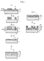
- a lower lift-off film 2 composed of polyimide-based resin having the following unit structural formula X is applied to a thickness of 10 ⁇ m to a Si substrate 1 and hardened by heat treatment in vacuum according to the heat pattern shown in Fig. 3.
- an upper lift-off film 3 composed of polyimide-based resin having the following unit structural formula Y is applied to a thickness of 3 ⁇ m to the surface of the lower lift-off film 2 , and likewise hardened by heat treatment according to the heat pattern shown in Fig. 3.
- masks 4 composed of SiO2 are formed to a thickness of about 1 ⁇ m on the upper lift-off film 3 by sputtering and patterning is carried out with a photoresist [Fig. 1(A)].
- the photoresist is removed, and then the lower lift-off film 2 and the upper lift-off film 3 are dry etched with O2 plasma to form a wiring pattern [Fig. 1(B)].
- wiring conductors 5 composed of Cu are vapor deposited to a thickness of 10 ⁇ m at a substrate temperature of 200°C [Fig. 1(C)].
- the substrate 1 is dipped in an etching solution composed of hydrazine and ethylenediamine at a mixing ratio of 1:1 by mole for 30 minutes to remove the upper lift-off film 3 by lifting off [Fig. 1(D)]. In this manner, the first wiring layer is formed.
- a lower lift-off film 2a composed of the polyimide based resin having the unit structural formula X is formed on the lower lift-off film 2 and the first layer of wiring conductor 5 , and then an upper-off film 3a composed of the polyimide-based resin having the unit structural formual Y and then a mask 4a for dry etching are formed thereon in the same manner as in Fig. 1(A).
- dry etching is carried out with O2 plasma and the lift-off films 2a and 3a are patterned to form a through-hole 6 for connecting the first layer of wiring conductor 5 to a second layer of wiring conductor to be successively formed [Fig. 1(E)].
- a lower lift-off film 2b composed of polyimide-based resin having the unit structural formula X is formed on the lower lift-off film 2a composed of the polyimide-based resin having the unit structural formula X, and then an upper lift-off film 3b composed of polyimide-based resin having the unit structural formula Y and a mask 4b for dry etching, composed of a SiO2 sputtered mask, are formed thereon successively.
- the upper and lower lift-off films are patterned according to the wiring pattern of the second layer [Fig. 1(G)].
- a wiring conductor 5a composed of Cu for a second layer is vapor deposited, and the upper lift-off film 3b is removed (lifted off) by the etching solution, whereby a second wiring layer is formed.
- Fig. 2 is a cross-sectional view of finally formed wiring.
- the second layer of lift-off film can be flattened by leaving the lower lift-off film used for forming the first layer of wiring and making the thickness of the lower lift-off film equal to that of the first layer of wiring.
- the etching of lift-off film proceeds uniformly throughout the entire surface and a desired wiring pattern can be patterned.
- Fig. 5(A) shows the state where the first layer of lower lift-off film 2 is removed off
- Fig. 5(B) shows the state where a lower lift-off film 2a and an upper lift-off film 3a are formed from the state of Fig. 5(A). It can be seen therefrom that the lift-off films 2a and 3a cannot be flattened.
- a lift-off film 3 composed of polyimide-based resin having the unit structural formula Y is applied to a thickness of 15 ⁇ m to a Si substrate 1 , and hardened by heat treatment according to the heat pattern of Fig. 3. Then, SiO2 sputtered films 4 are formed thereon.
- the lift-off film 3 is patterened by dry etching with O2 plasma [Fig. 7(B)].
- the patterning may be a wet etching with an etching solution.
- wiring conductors 5 composed of Cu are vapor deposited to a thickness of 15 ⁇ m after the SiO2 mask 4 has been removed or while retaining the SiO2 mask 4 [Fig. 6(C)].
- Fig. 4 shows a process for forming a wiring with polyimide-based resin having the unit structural formula X as a lift-off material.
- a lift-off film 11 composed of polyimide-based resin having the unit structural formula X as a lift-off material is formed on a Si substrate 10 [Fig. 4(A)].
- the lift-off film 11 is hardened by heat treatment according to the heat pattern of Fig. 3 and masks 12 composed of Cr and resists 13 are laid successively thereon to make masking [Fig. 4(B)].
- a wiring pattern is formed on the substrate 10 by dry etching with O2 plasma [Fig. 4(C)].
- Wiring conductors 14 composed of Cu or Al are vapor deposited thereon [Fig. 4(D).
- the lift-off film 11 is removed (lifted off) by O2 plasma usher treatment, while leaving only conductor 14 as a wiring on the substrate 10 .
- lifting off must be carried out by dry etching because of poor wet etching susceptibility of polyimide-based resin having the unit structural formula X, and also there remain residues of the lift-off film. Furthermore, it is impossible to form a wiring film as thick as 10-20 ⁇ m.
- a wiring film as thick as 10-20 ⁇ m can be readily lifted off with an etching solution when polyimide-based resin having the unit structural formula Y is used.
- polyimide-based resin having the unit structural formula X as a lower lift-off film
- polyimide-based resin having the unit structural formula Y as an upper lift-off film
- lift-off films can be flattened in the multiple layer wiring and the wiring pattern precision can be enhanced.
Landscapes
- Engineering & Computer Science (AREA)
- Manufacturing & Machinery (AREA)
- Microelectronics & Electronic Packaging (AREA)
- Internal Circuitry In Semiconductor Integrated Circuit Devices (AREA)
- Production Of Multi-Layered Print Wiring Board (AREA)
- Manufacturing Of Printed Circuit Boards (AREA)
- Weting (AREA)
Applications Claiming Priority (2)
| Application Number | Priority Date | Filing Date | Title |
|---|---|---|---|
| JP200971/86 | 1986-08-27 | ||
| JP20097186 | 1986-08-27 |
Publications (3)
| Publication Number | Publication Date |
|---|---|
| EP0261400A2 true EP0261400A2 (de) | 1988-03-30 |
| EP0261400A3 EP0261400A3 (en) | 1989-05-24 |
| EP0261400B1 EP0261400B1 (de) | 1992-10-28 |
Family
ID=16433363
Family Applications (1)
| Application Number | Title | Priority Date | Filing Date |
|---|---|---|---|
| EP87112098A Expired - Lifetime EP0261400B1 (de) | 1986-08-27 | 1987-08-20 | "Lift-off" Verfahren zur Herstellung von Leiterbahnen auf einem Substrat |
Country Status (5)
| Country | Link |
|---|---|
| US (1) | US4886573A (de) |
| EP (1) | EP0261400B1 (de) |
| JP (1) | JPH07120647B2 (de) |
| KR (1) | KR940009174B1 (de) |
| DE (1) | DE3782389T2 (de) |
Cited By (3)
| Publication number | Priority date | Publication date | Assignee | Title |
|---|---|---|---|---|
| EP0424805A3 (en) * | 1989-10-26 | 1991-07-17 | Occidental Chemical Corporation | Copolyimide odpa/bpda/4,4'-oda/p-pda |
| EP0421053A3 (en) * | 1989-10-06 | 1992-06-10 | International Business Machines Corporation | High temperature lift-off process |
| WO2006132379A3 (en) * | 2005-06-07 | 2007-05-03 | Fujifilm Corp | Structure for functional film pattern formation and method of manufacturing functional film |
Families Citing this family (10)
| Publication number | Priority date | Publication date | Assignee | Title |
|---|---|---|---|---|
| US5198298A (en) * | 1989-10-24 | 1993-03-30 | Advanced Micro Devices, Inc. | Etch stop layer using polymers |
| US5426071A (en) * | 1994-03-04 | 1995-06-20 | E. I. Du Pont De Nemours And Company | Polyimide copolymer film for lift-off metallization |
| US6303488B1 (en) | 1997-02-12 | 2001-10-16 | Micron Technology, Inc. | Semiconductor processing methods of forming openings to devices and substrates, exposing material from which photoresist cannot be substantially selectively removed |
| US6495468B2 (en) | 1998-12-22 | 2002-12-17 | Micron Technology, Inc. | Laser ablative removal of photoresist |
| KR100643404B1 (ko) * | 2005-09-22 | 2006-11-10 | 삼성전자주식회사 | 디스플레이장치 및 그 제조방법 |
| US7993972B2 (en) * | 2008-03-04 | 2011-08-09 | Stats Chippac, Ltd. | Wafer level die integration and method therefor |
| JP5786548B2 (ja) * | 2011-08-15 | 2015-09-30 | 住友電気工業株式会社 | 窒化物半導体発光素子を作製する方法 |
| JP2013243263A (ja) * | 2012-05-21 | 2013-12-05 | Internatl Business Mach Corp <Ibm> | 3次元積層パッケージにおける電力供給と放熱(冷却)との両立 |
| KR102614588B1 (ko) * | 2018-08-20 | 2023-12-18 | 삼성디스플레이 주식회사 | 표시 장치의 제조 방법 |
| CN113632182B (zh) * | 2019-03-29 | 2022-12-30 | 株式会社自动网络技术研究所 | 布线模块 |
Family Cites Families (21)
| Publication number | Priority date | Publication date | Assignee | Title |
|---|---|---|---|---|
| US3179633A (en) * | 1962-01-26 | 1965-04-20 | Du Pont | Aromatic polyimides from meta-phenylene diamine and para-phenylene diamine |
| GB1230421A (de) * | 1967-09-15 | 1971-05-05 | ||
| US4218283A (en) * | 1974-08-23 | 1980-08-19 | Hitachi, Ltd. | Method for fabricating semiconductor device and etchant for polymer resin |
| JPS52156583A (en) * | 1976-06-23 | 1977-12-27 | Hitachi Ltd | Electrode formation method in semiconductor device |
| FR2392495A1 (fr) * | 1977-05-25 | 1978-12-22 | Radiotechnique Compelec | Procede de realisation de dispositifs semi-conducteurs a reseau de conducteurs mono ou multicouche et dispositifs ainsi obtenus |
| JPS54138068A (en) * | 1978-04-18 | 1979-10-26 | Toray Ind Inc | Polyimide film |
| JPS5527326A (en) * | 1978-08-17 | 1980-02-27 | Ube Ind Ltd | Polyimide resin composition and its preparation |
| EP0019391B1 (de) * | 1979-05-12 | 1982-10-06 | Fujitsu Limited | Verfahren zur Herstellung einer elektronischen Vorrichtung mit Vielschicht-Verdrahtungsstruktur |
| US4367119A (en) * | 1980-08-18 | 1983-01-04 | International Business Machines Corporation | Planar multi-level metal process with built-in etch stop |
| JPS5744618A (en) * | 1980-08-29 | 1982-03-13 | Hitachi Chem Co Ltd | Preparation of polyimide copolymer |
| JPS5792849A (en) * | 1980-12-01 | 1982-06-09 | Mitsubishi Electric Corp | Manufacture of semiconductor device |
| US4451971A (en) * | 1982-08-02 | 1984-06-05 | Fairchild Camera And Instrument Corporation | Lift-off wafer processing |
| US4428796A (en) * | 1982-08-02 | 1984-01-31 | Fairchild Camera And Instrument Corporation | Adhesion bond-breaking of lift-off regions on semiconductor structures |
| US4497684A (en) * | 1983-02-22 | 1985-02-05 | Amdahl Corporation | Lift-off process for depositing metal on a substrate |
| EP0133533B1 (de) * | 1983-08-01 | 1993-04-21 | Hitachi, Ltd. | Harzmaterial mit geringer thermischer Ausdehnung für Verdrahtungsisolationsfolie |
| JPS60110140A (ja) * | 1983-11-21 | 1985-06-15 | Hitachi Ltd | 配線構造体形成方法 |
| JPS60120723A (ja) * | 1983-11-30 | 1985-06-28 | インタ−ナショナル ビジネス マシ−ンズ コ−ポレ−ション | 電子装置 |
| JPS60157286A (ja) * | 1984-01-27 | 1985-08-17 | 株式会社日立製作所 | フレキシブルプリント基板の製造方法 |
| JPS60212428A (ja) * | 1984-04-06 | 1985-10-24 | Mitsui Toatsu Chem Inc | ポリイミド樹脂プレポリマ溶液の調整方法 |
| US4519872A (en) * | 1984-06-11 | 1985-05-28 | International Business Machines Corporation | Use of depolymerizable polymers in the fabrication of lift-off structure for multilevel metal processes |
| US4606998A (en) * | 1985-04-30 | 1986-08-19 | International Business Machines Corporation | Barrierless high-temperature lift-off process |
-
1987
- 1987-08-19 US US07/087,021 patent/US4886573A/en not_active Expired - Fee Related
- 1987-08-20 EP EP87112098A patent/EP0261400B1/de not_active Expired - Lifetime
- 1987-08-20 DE DE8787112098T patent/DE3782389T2/de not_active Expired - Fee Related
- 1987-08-26 JP JP62210107A patent/JPH07120647B2/ja not_active Expired - Lifetime
- 1987-08-26 KR KR87009328A patent/KR940009174B1/ko not_active Expired - Fee Related
Cited By (3)
| Publication number | Priority date | Publication date | Assignee | Title |
|---|---|---|---|---|
| EP0421053A3 (en) * | 1989-10-06 | 1992-06-10 | International Business Machines Corporation | High temperature lift-off process |
| EP0424805A3 (en) * | 1989-10-26 | 1991-07-17 | Occidental Chemical Corporation | Copolyimide odpa/bpda/4,4'-oda/p-pda |
| WO2006132379A3 (en) * | 2005-06-07 | 2007-05-03 | Fujifilm Corp | Structure for functional film pattern formation and method of manufacturing functional film |
Also Published As
| Publication number | Publication date |
|---|---|
| EP0261400A3 (en) | 1989-05-24 |
| US4886573A (en) | 1989-12-12 |
| EP0261400B1 (de) | 1992-10-28 |
| KR940009174B1 (en) | 1994-10-01 |
| JPS63170925A (ja) | 1988-07-14 |
| JPH07120647B2 (ja) | 1995-12-20 |
| DE3782389D1 (de) | 1992-12-03 |
| DE3782389T2 (de) | 1993-05-06 |
| KR880003550A (ko) | 1988-05-17 |
Similar Documents
| Publication | Publication Date | Title |
|---|---|---|
| EP0261400A2 (de) | "Lift-off" Verfahren zur Herstellung von Leiterbahnen auf einem Substrat | |
| US5277749A (en) | Methods and apparatus for relieving stress and resisting stencil delamination when performing lift-off processes that utilize high stress metals and/or multiple evaporation steps | |
| US4692205A (en) | Silicon-containing polyimides as oxygen etch stop and dual dielectric coatings | |
| US4202914A (en) | Method of depositing thin films of small dimensions utilizing silicon nitride lift-off mask | |
| EP0099544B1 (de) | Verfahren zum Herstellen von Leiterbahnen und Durchgangsverbindungen auf LSI-Trägern | |
| US6297171B1 (en) | Semiconductor processing method of promoting photoresist adhesion to an outer substrate layer predominately comprising silicon nitride | |
| EP0054663A1 (de) | Verfahren zum Herstellen eines Metallmusters auf Kupferbasis | |
| EP0137927A2 (de) | Verfahren zum kontrollierten Ätzen von spitz zulaufenden Löchern in dielektrischen Borosilikatgläsern | |
| JP2004513515A (ja) | ホトレジストの改良形接着用アモルファス炭素層 | |
| US5907791A (en) | Method of making semiconductor devices by patterning a wafer having a non-planar surface | |
| EP0073910B1 (de) | Verfahren zum Ätzen von Polyimiden | |
| US4226932A (en) | Titanium nitride as one layer of a multi-layered coating intended to be etched | |
| JPH01137635A (ja) | 反応性イオン・エツチングによって基板材料にパターンを転写する方法 | |
| US4502916A (en) | Process for forming fine patterns | |
| US5126007A (en) | Method for etching a pattern in layer of gold | |
| US4830706A (en) | Method of making sloped vias | |
| EP0132585B1 (de) | Abhebeverfahren und Zusammensetzung dafür | |
| KR100230405B1 (ko) | 반도체장치의 다층 배선 형성방법 | |
| US5270151A (en) | Spin on oxygen reactive ion etch barrier | |
| JPS6392102A (ja) | フレキシブルなマイクロ回路の製造方法 | |
| JPH058856B2 (de) | ||
| JPH0629647A (ja) | フォトレジストの剥離方法 | |
| JP2770653B2 (ja) | 半導体集積回路装置の製造方法 | |
| KR100252757B1 (ko) | 금속패턴 형성방법 | |
| KR20010076614A (ko) | 멀티칩모듈 기판 제조공정에서 전기도금에 의한 금속배선제조방법 |
Legal Events
| Date | Code | Title | Description |
|---|---|---|---|
| PUAI | Public reference made under article 153(3) epc to a published international application that has entered the european phase |
Free format text: ORIGINAL CODE: 0009012 |
|
| AK | Designated contracting states |
Kind code of ref document: A2 Designated state(s): DE FR GB |
|
| RHK1 | Main classification (correction) |
Ipc: H01L 21/312 |
|
| PUAL | Search report despatched |
Free format text: ORIGINAL CODE: 0009013 |
|
| AK | Designated contracting states |
Kind code of ref document: A3 Designated state(s): DE FR GB |
|
| 17P | Request for examination filed |
Effective date: 19890608 |
|
| 17Q | First examination report despatched |
Effective date: 19910419 |
|
| GRAA | (expected) grant |
Free format text: ORIGINAL CODE: 0009210 |
|
| AK | Designated contracting states |
Kind code of ref document: B1 Designated state(s): DE FR GB |
|
| REF | Corresponds to: |
Ref document number: 3782389 Country of ref document: DE Date of ref document: 19921203 |
|
| ET | Fr: translation filed | ||
| PLBE | No opposition filed within time limit |
Free format text: ORIGINAL CODE: 0009261 |
|
| STAA | Information on the status of an ep patent application or granted ep patent |
Free format text: STATUS: NO OPPOSITION FILED WITHIN TIME LIMIT |
|
| 26N | No opposition filed | ||
| PGFP | Annual fee paid to national office [announced via postgrant information from national office to epo] |
Ref country code: FR Payment date: 19960625 Year of fee payment: 10 |
|
| PGFP | Annual fee paid to national office [announced via postgrant information from national office to epo] |
Ref country code: GB Payment date: 19960627 Year of fee payment: 10 |
|
| PGFP | Annual fee paid to national office [announced via postgrant information from national office to epo] |
Ref country code: DE Payment date: 19960930 Year of fee payment: 10 |
|
| PG25 | Lapsed in a contracting state [announced via postgrant information from national office to epo] |
Ref country code: GB Free format text: LAPSE BECAUSE OF NON-PAYMENT OF DUE FEES Effective date: 19970820 |
|
| GBPC | Gb: european patent ceased through non-payment of renewal fee |
Effective date: 19970820 |
|
| PG25 | Lapsed in a contracting state [announced via postgrant information from national office to epo] |
Ref country code: FR Free format text: LAPSE BECAUSE OF NON-PAYMENT OF DUE FEES Effective date: 19980430 |
|
| PG25 | Lapsed in a contracting state [announced via postgrant information from national office to epo] |
Ref country code: DE Free format text: LAPSE BECAUSE OF NON-PAYMENT OF DUE FEES Effective date: 19980501 |
|
| REG | Reference to a national code |
Ref country code: FR Ref legal event code: ST |