EP0235682A2 - Corps frité à base de nitrure d'aluminium, muni d'une couche métallisée conductrice - Google Patents
Corps frité à base de nitrure d'aluminium, muni d'une couche métallisée conductrice Download PDFInfo
- Publication number
- EP0235682A2 EP0235682A2 EP87102344A EP87102344A EP0235682A2 EP 0235682 A2 EP0235682 A2 EP 0235682A2 EP 87102344 A EP87102344 A EP 87102344A EP 87102344 A EP87102344 A EP 87102344A EP 0235682 A2 EP0235682 A2 EP 0235682A2
- Authority
- EP
- European Patent Office
- Prior art keywords
- group
- sintered body
- elements
- conductive
- metallized layer
- Prior art date
- Legal status (The legal status is an assumption and is not a legal conclusion. Google has not performed a legal analysis and makes no representation as to the accuracy of the status listed.)
- Granted
Links
Images

Classifications
-
- C—CHEMISTRY; METALLURGY
- C04—CEMENTS; CONCRETE; ARTIFICIAL STONE; CERAMICS; REFRACTORIES
- C04B—LIME, MAGNESIA; SLAG; CEMENTS; COMPOSITIONS THEREOF, e.g. MORTARS, CONCRETE OR LIKE BUILDING MATERIALS; ARTIFICIAL STONE; CERAMICS; REFRACTORIES; TREATMENT OF NATURAL STONE
- C04B41/00—After-treatment of mortars, concrete, artificial stone or ceramics; Treatment of natural stone
- C04B41/80—After-treatment of mortars, concrete, artificial stone or ceramics; Treatment of natural stone of only ceramics
- C04B41/81—Coating or impregnation
- C04B41/85—Coating or impregnation with inorganic materials
- C04B41/87—Ceramics
-
- C—CHEMISTRY; METALLURGY
- C04—CEMENTS; CONCRETE; ARTIFICIAL STONE; CERAMICS; REFRACTORIES
- C04B—LIME, MAGNESIA; SLAG; CEMENTS; COMPOSITIONS THEREOF, e.g. MORTARS, CONCRETE OR LIKE BUILDING MATERIALS; ARTIFICIAL STONE; CERAMICS; REFRACTORIES; TREATMENT OF NATURAL STONE
- C04B41/00—After-treatment of mortars, concrete, artificial stone or ceramics; Treatment of natural stone
- C04B41/45—Coating or impregnating, e.g. injection in masonry, partial coating of green or fired ceramics, organic coating compositions for adhering together two concrete elements
- C04B41/50—Coating or impregnating, e.g. injection in masonry, partial coating of green or fired ceramics, organic coating compositions for adhering together two concrete elements with inorganic materials
- C04B41/5053—Coating or impregnating, e.g. injection in masonry, partial coating of green or fired ceramics, organic coating compositions for adhering together two concrete elements with inorganic materials non-oxide ceramics
- C04B41/5062—Borides, Nitrides or Silicides
- C04B41/5063—Aluminium nitride
-
- C—CHEMISTRY; METALLURGY
- C04—CEMENTS; CONCRETE; ARTIFICIAL STONE; CERAMICS; REFRACTORIES
- C04B—LIME, MAGNESIA; SLAG; CEMENTS; COMPOSITIONS THEREOF, e.g. MORTARS, CONCRETE OR LIKE BUILDING MATERIALS; ARTIFICIAL STONE; CERAMICS; REFRACTORIES; TREATMENT OF NATURAL STONE
- C04B41/00—After-treatment of mortars, concrete, artificial stone or ceramics; Treatment of natural stone
- C04B41/45—Coating or impregnating, e.g. injection in masonry, partial coating of green or fired ceramics, organic coating compositions for adhering together two concrete elements
- C04B41/50—Coating or impregnating, e.g. injection in masonry, partial coating of green or fired ceramics, organic coating compositions for adhering together two concrete elements with inorganic materials
- C04B41/5053—Coating or impregnating, e.g. injection in masonry, partial coating of green or fired ceramics, organic coating compositions for adhering together two concrete elements with inorganic materials non-oxide ceramics
- C04B41/5062—Borides, Nitrides or Silicides
- C04B41/5068—Titanium nitride
-
- C—CHEMISTRY; METALLURGY
- C04—CEMENTS; CONCRETE; ARTIFICIAL STONE; CERAMICS; REFRACTORIES
- C04B—LIME, MAGNESIA; SLAG; CEMENTS; COMPOSITIONS THEREOF, e.g. MORTARS, CONCRETE OR LIKE BUILDING MATERIALS; ARTIFICIAL STONE; CERAMICS; REFRACTORIES; TREATMENT OF NATURAL STONE
- C04B41/00—After-treatment of mortars, concrete, artificial stone or ceramics; Treatment of natural stone
- C04B41/45—Coating or impregnating, e.g. injection in masonry, partial coating of green or fired ceramics, organic coating compositions for adhering together two concrete elements
- C04B41/50—Coating or impregnating, e.g. injection in masonry, partial coating of green or fired ceramics, organic coating compositions for adhering together two concrete elements with inorganic materials
- C04B41/51—Metallising, e.g. infiltration of sintered ceramic preforms with molten metal
- C04B41/5133—Metallising, e.g. infiltration of sintered ceramic preforms with molten metal with a composition mainly composed of one or more of the refractory metals
-
- C—CHEMISTRY; METALLURGY
- C04—CEMENTS; CONCRETE; ARTIFICIAL STONE; CERAMICS; REFRACTORIES
- C04B—LIME, MAGNESIA; SLAG; CEMENTS; COMPOSITIONS THEREOF, e.g. MORTARS, CONCRETE OR LIKE BUILDING MATERIALS; ARTIFICIAL STONE; CERAMICS; REFRACTORIES; TREATMENT OF NATURAL STONE
- C04B41/00—After-treatment of mortars, concrete, artificial stone or ceramics; Treatment of natural stone
- C04B41/80—After-treatment of mortars, concrete, artificial stone or ceramics; Treatment of natural stone of only ceramics
- C04B41/81—Coating or impregnation
- C04B41/85—Coating or impregnation with inorganic materials
- C04B41/88—Metals
-
- H—ELECTRICITY
- H10—SEMICONDUCTOR DEVICES; ELECTRIC SOLID-STATE DEVICES NOT OTHERWISE PROVIDED FOR
- H10W—GENERIC PACKAGES, INTERCONNECTIONS, CONNECTORS OR OTHER CONSTRUCTIONAL DETAILS OF DEVICES COVERED BY CLASS H10
- H10W70/00—Package substrates; Interposers; Redistribution layers [RDL]
- H10W70/01—Manufacture or treatment
- H10W70/05—Manufacture or treatment of insulating or insulated package substrates, or of interposers, or of redistribution layers
-
- H—ELECTRICITY
- H10—SEMICONDUCTOR DEVICES; ELECTRIC SOLID-STATE DEVICES NOT OTHERWISE PROVIDED FOR
- H10W—GENERIC PACKAGES, INTERCONNECTIONS, CONNECTORS OR OTHER CONSTRUCTIONAL DETAILS OF DEVICES COVERED BY CLASS H10
- H10W70/00—Package substrates; Interposers; Redistribution layers [RDL]
- H10W70/60—Insulating or insulated package substrates; Interposers; Redistribution layers
- H10W70/62—Insulating or insulated package substrates; Interposers; Redistribution layers characterised by their interconnections
- H10W70/66—Conductive materials thereof
-
- H—ELECTRICITY
- H10—SEMICONDUCTOR DEVICES; ELECTRIC SOLID-STATE DEVICES NOT OTHERWISE PROVIDED FOR
- H10W—GENERIC PACKAGES, INTERCONNECTIONS, CONNECTORS OR OTHER CONSTRUCTIONAL DETAILS OF DEVICES COVERED BY CLASS H10
- H10W70/00—Package substrates; Interposers; Redistribution layers [RDL]
- H10W70/60—Insulating or insulated package substrates; Interposers; Redistribution layers
- H10W70/67—Insulating or insulated package substrates; Interposers; Redistribution layers characterised by their insulating layers or insulating parts
- H10W70/69—Insulating materials thereof
- H10W70/692—Ceramics or glasses
-
- H—ELECTRICITY
- H05—ELECTRIC TECHNIQUES NOT OTHERWISE PROVIDED FOR
- H05K—PRINTED CIRCUITS; CASINGS OR CONSTRUCTIONAL DETAILS OF ELECTRIC APPARATUS; MANUFACTURE OF ASSEMBLAGES OF ELECTRICAL COMPONENTS
- H05K1/00—Printed circuits
- H05K1/02—Details
- H05K1/09—Use of materials for the conductive, e.g. metallic pattern
- H05K1/092—Dispersed materials, e.g. conductive pastes or inks
-
- Y—GENERAL TAGGING OF NEW TECHNOLOGICAL DEVELOPMENTS; GENERAL TAGGING OF CROSS-SECTIONAL TECHNOLOGIES SPANNING OVER SEVERAL SECTIONS OF THE IPC; TECHNICAL SUBJECTS COVERED BY FORMER USPC CROSS-REFERENCE ART COLLECTIONS [XRACs] AND DIGESTS
- Y10—TECHNICAL SUBJECTS COVERED BY FORMER USPC
- Y10S—TECHNICAL SUBJECTS COVERED BY FORMER USPC CROSS-REFERENCE ART COLLECTIONS [XRACs] AND DIGESTS
- Y10S428/00—Stock material or miscellaneous articles
- Y10S428/901—Printed circuit
-
- Y—GENERAL TAGGING OF NEW TECHNOLOGICAL DEVELOPMENTS; GENERAL TAGGING OF CROSS-SECTIONAL TECHNOLOGIES SPANNING OVER SEVERAL SECTIONS OF THE IPC; TECHNICAL SUBJECTS COVERED BY FORMER USPC CROSS-REFERENCE ART COLLECTIONS [XRACs] AND DIGESTS
- Y10—TECHNICAL SUBJECTS COVERED BY FORMER USPC
- Y10T—TECHNICAL SUBJECTS COVERED BY FORMER US CLASSIFICATION
- Y10T428/00—Stock material or miscellaneous articles
- Y10T428/24—Structurally defined web or sheet [e.g., overall dimension, etc.]
- Y10T428/24802—Discontinuous or differential coating, impregnation or bond [e.g., artwork, printing, retouched photograph, etc.]
- Y10T428/24917—Discontinuous or differential coating, impregnation or bond [e.g., artwork, printing, retouched photograph, etc.] including metal layer
-
- Y—GENERAL TAGGING OF NEW TECHNOLOGICAL DEVELOPMENTS; GENERAL TAGGING OF CROSS-SECTIONAL TECHNOLOGIES SPANNING OVER SEVERAL SECTIONS OF THE IPC; TECHNICAL SUBJECTS COVERED BY FORMER USPC CROSS-REFERENCE ART COLLECTIONS [XRACs] AND DIGESTS
- Y10—TECHNICAL SUBJECTS COVERED BY FORMER USPC
- Y10T—TECHNICAL SUBJECTS COVERED BY FORMER US CLASSIFICATION
- Y10T428/00—Stock material or miscellaneous articles
- Y10T428/24—Structurally defined web or sheet [e.g., overall dimension, etc.]
- Y10T428/24802—Discontinuous or differential coating, impregnation or bond [e.g., artwork, printing, retouched photograph, etc.]
- Y10T428/24926—Discontinuous or differential coating, impregnation or bond [e.g., artwork, printing, retouched photograph, etc.] including ceramic, glass, porcelain or quartz layer
Definitions
- the present invention relates to an aluminium nitride sintered body, and more specifically to an aluminium nitride sintered body having a conductive metallized layer with an excellent high-temperature adhesion to the aluminium nitride sintered body base material and available for a semiconductor device substrate.
- the present invention relates to a circuit substrate using an aluminium nitride sintered body as an insulating layer, and more particular to a circuit substrate in which conductive layers are sintered integral and simultaneous with the insulating layer to realize a multilayer interconnection.
- aluminium nitride (AlN) sintered body has been noticed as various structure materials, various electronic/electric parts materials, etc. Recently, in particular, this A1N sintered body has been used in place of alumina (Al 2 O 3 ) and beryllia (BeO), because Al 2 O 3 is not satisfactory in heat radiation and BeO is poisonous and therefore complicated in handling this material.
- the body is usually joined with some metal members, so that a conductive metallized layer is generally formed on the surface of the A 1 N sintered body.
- DBC direct bond copper
- the conductive metallized layer formed on the surface of the A1N sintered body in accordance with the above-mentioned conventional methods is weak in adhesion to the AlN sintered body, in particular at high temperature. Therefore, there exist problems such that it is difficult to bond another member with the formed metallized layer by a high temperature (700°C or higher) bonding method such as brazing, high temperature soldering, etc. or, even if bonded, when the AlN sintered body to which another member is bonded is used at high temperature, the formed metallized layer is peeled off from the surface of the sintered body and eventually another member is dropped off from the metallized layer.
- a high temperature (700°C or higher) bonding method such as brazing, high temperature soldering, etc.
- the A1N sintered body including a conductive metallized layer is used as a heat radiation substrate for electronic circuits, since the substrate is subjected to temperature changes (heat cycles) from low to high or vice versa, there exists another disadvantage such that cracks develop in the metallized layer due to a difference in thermal expansion coefficient between the A1N and the metallized layer forming component.
- This AIN sintered body is manufactured roughly as follows: An AlN powder is first mixed with a sintering aid such as Y 2 0 3 , Sm 2 O 3 , CaO, etc. of a predetermined amount, and further with an acrylic base resin binder, if necessary as an aid. These are sufficiently mixed, formed into an AlN green sheet body (raw compact) of a predetermined shape under pressure, and sintered at a predetermined temperature within a nitride atmosphere, for instance.
- a sintering aid such as Y 2 0 3 , Sm 2 O 3 , CaO, etc.
- this film was a metallized layer of Cu, A u or A g-Pd formed on the surface of the A1N sintered body in accordance with the DBC (direct bond cupper) method or the thick film method.
- the second problem occurs when a semiconductor element or wire is brazed or soldered at a high temperature onto the formed metallized layer. That is to say, although brazing is effected at about 800°C with a hydrogen-nitrogen mixture gas, since the metallized layer baking temperature is as low as about 600 to 1000°C, the adhesion junction strength between the metallized layer and the A1N sintered body surface is lowered markedly in brazing, thus disabling brazing in practice. Further, the similar problem arises in the case of high temperature soldering.
- the third problem occurs due to a difference in thermal expansion coefficient between the AlN sintered body and the metallized layer.
- brazing and high temperature soldering severe heat-cool cycles are applied in use to the substrate on which semiconductor elements such as silicon wafers are mounted.
- thermal stresses are generated on junction surfaces between AlN sintered body, metallized layer, brazed layer (or soldered layer), and semiconductor elements due to differences in thermal expansion coefficient between two of these layers, thus resulting in an occurrence of peelings of these elements, as shown in Fig. 1 B .
- the thermal expansion coefficient of the metallized layer is about 2 to 4 times greater than that (about 4.6 x 10 -6 /°C) of the AlN sintered body, and roughly equal to or half of that of brazed or soldered layer. Therefore, since there exists a big difference between the AlN sintered body and the metallized layer or the brazed (soldered) layer, microcracks are readily produced on the boundary surface between the A l N sintered body and the metallized layer or the brazed (or soldered) layer during heat cycle. Further, these microcracks develop gradually when the heat cycle is repeated, thus finally causing the peeling-off of the semiconductor element from the sintered body. This problem is serious, in particular, because the reliability of appliances having substrates on which semiconductor elements are mounted will be deteriorated.
- the fourth problem is that the adhesion strength between the metallized layer and the AlN sintered body is small at high temperatures, so that the reliability of the substrate is low at high temperature as in the second problem.
- the fifth problem is that thermal energy is not economical when checking the manufacturing processes from the first to the last.
- the substrate is completed by first sintering an A1N green body and further sintering the A1N sintered body again to form the metallized layer.
- Al 2 O 3 ceramics have widely been adopted as an insulating material for circuit substrates.
- Al 2 O 3 is low in heat conductivity, there still exists a problem with heat radiation. Therefore, it has been studied to apply A1N ceramics excellent in electrical characteristics such as electric insulating characteristics (as an insulator) and in thermal conductivity to circuit substrates (as disclosed Japanese Published Unexamined Pat. Appl. No. 60-178688).
- an aluminium nitride sintered body having a conductive metallized layer high in adhesion strength particularly at high temperature within a reducing atmosphere and therefore high in adhesion reliability of when other members are bonded to the metallized layer by brazing or soldering.
- an aluminium nitride sintered body comprises: (a) an insulating layer formed by sintering an aluminium nitride body; and (b) a metallized layer formed on said insulating layer, said metallized layer including as component (1) a conductor element; and (2) at least one element selected from the group consisting of IIa, IIIa, IVa, IIIb, lanthanide and actinoide group elements in periodic law table.
- the insulating layer includes at least one element selected from the group consisting of alkaline earth and rare-earth elements as a sintering aid to enable atmospheric sintering and to increase adhesion strength between said two layers.
- the conductor is any one of W, Mo, Ta, TiN and ZrN. Further, the content of the sintering aid in the insulating layer is 20 wt.% or less in oxide conversion, preferably 0.05 wt.% or more.
- the feature of the present invention exists in combination of the conductor and the component element. Therefore, the ratio of both is not limitative, but selectively determined according to the various objects of improving the adhesion strength between the two layers, the conductivity of the conductor, the deformation of the sintered body in sintering process, and the like.
- An embodiment of the aluminium nitride sintered body according to the present invention for providing a stronger adhesion strength comprises a conductive metallized layer on at least a part of an insulating layer of AlN sintered body, the conductive metallized layer including:
- the A1N sintered body according to the present invention is characterized by the combination of component elements for composing the phase of the conductive metallized layer formed on the sintered body base material (corresponding to the insulating layer) surface, so that the properties of the AlN sintered body base material itself are not particularly limited.
- the elements belonging to the first group of molybdenum (Mo), tungsten (W) and tantalum (Ta) are excellent in heat resistance and further approximate to the A1N sintered body base material in thermal expansion coefficient, so that these elements serve to improve the heat resistance characteristics and the cyclic heat resistance characteristics.
- these elements are included in a filler of the metallized layer as a single element or a combination of two or more elements.
- these elements belonging to the first group exist ih the metallized layer in the form of each element, a compound or solid solution including each element, or a mixture of two or more elements selected from the group consisting of these elements, compounds and solid solutions.
- the compounds are oxides of these elements, nitrides thereof, carbides thereof, acid nitrides thereof, carbonic nitrides thereof, carbonic oxides thereof, carbonic acid nitrides thereof, borides thereof, silicides thereof, etc.
- these compounds can be composite compounds or solid solutions which include at least one of elements belonging to the second group (described later) and/or at least one of elements other than those belonging to the second group.
- Mo exists in the composed phase of the conductive metallized layer in the form of Mo or Mo-Al solid solution.
- the elements belonging to the second group of the IIIb group elements B, Al, Ga, In, Tl), the IVa group elements (Ti, Zr, Hf), IIIa group elements (Sc, Y, Te), the rare earth elements (Y, La, Ce, Pr, Nd, Pm, Sm, Eu, Gd, Tb, Dy, Ho, Er, Tm, Yb, Lu) and the actinoid (Ac, Th, Pa, U, Np, Pu, Am, Cm, Bk, Cf, Es, Fm, Md, No, Lr) are excellent in weatness relative to AlN, so that these elements serve to improve the adhesion between the conductive metallized layer and the A1N sintered body.
- Al, Ti, Zr, Hf, Y, Ce, Dy, Th, Sm are particularly preferable as the elements belonging to the second group.
- these elements belonging to the second group are included in the composed phase of the metallized layer in the form of a single element or a mixture of two or more elements. That is, these elements exist in the metallized layer in the form of each element, a compound or solid solution including each element or a mixture of two or more elements selected from the group consisting of these elements, compounds and solid solutions.
- Ti exists in the composed phase of the conductive metallized layer in the form of T i N , T i0 2 , etc.
- the composition ratio of elements belonging to the first group and those belonging to the second group is not defined specifically.
- the ratio is appropriately determined according to the kind of elements used or the combination. For instance, it is preferable that the ratio of the sum total of the elements belonging to the first group to that of the elements belonging to the second group is 90/10 to 10/90 in atomic ratio.
- the AIN sintered body according to the present invention can be manufactured as follows:
- the paste or liquid applied on the surface of the AIN sintered body is dried and heat treated to form a metallized layer.
- the heating temperature is usually 1100 to 1800°C, although being different from the kind and the combination of the component elements.
- the treatment gas is nitrogen gas, dry forming gas, wet forming gas, etc.
- the treatment time is 0.5 to 2 hours, preferably. Where necessary, a plurality of these A1N sintered bodies on each surface of which the paste is applied to form a conductive layer are stacked one above the other for simultaneous sintering so as to provide multilayer interconnection.
- Ni plating for instance, is effected on the conductive metallized layer and then the plating layer is annealed at 600 to 850°C within a forming gas, before brazing or soldering. Further, it is possible to form an excellent metallized layer on the surface of the AlN sintered body by applying the paste already explained to an A1N green body and then sintering the both at the same time.
- a paste including at least one selected from the first group consisting of molybdenum (Mo), tungstn (W), tantalum (Ta), and compounds having at least one of these elements, and at least one selected from the second group consisting of III group elements in periodic law table, IVa group elements, rare earth elements (the rare earth elements are lanthanum family including Sc and Y), actinoide family elements, and compounds including at least one of these elements, is applied to an A1N green sheet body; and the whole is sintered simultaneously.
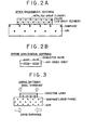
- FIG. 2A shows a model in which a conductive metallized layer including a first group metal element and a second group filler element is formed on an AlN sintered body including an assistant by simultaneous sintering.
- Fig. 2B shows an example in which two AlN green sheets each having two conductive paste layers are stacked one above the other before simultaneous sintering.
- the A1N green sheet body to which the present invention is applied is a raw compact obtained by mixing AlN powder of predetermined grain size with sintering assistant powder such as Y 2 0 2' YF 3' Sm 2 0 3 , or CaCO 3 and a binder such as wax or plastic at a predetermined ratio and by forming the mixture at room temperature under pressure or by forming the mixture into a sheet in accordance with doctor blade method.
- sintering assistant powder such as Y 2 0 2' YF 3' Sm 2 0 3 , or CaCO 3
- a binder such as wax or plastic
- the paste is composed of two components belonging to two groups I (conductor) and II (component elements) both conversed into a metallized layer after having been sintered and a medium for dispersing these components.
- the component belonging to the first group I is at least one selected from the group consisting of Mo, W, Ta, compounds including at least one of these elements.
- the component is a single metal of Mo, W, or Ta, these oxides, carbides, borides, silicides, acid nitride, carbon nitrides, hologenides, hydrides, hydroxides, nitrites, nitrates, sulfites sulfates, borates, carbonates, silicates, phosphates, phosphites, hydrochlorides, chlorates, oxalates, salts such as ammonium salt, alkoxycids such as ATRON NTa - 700 (Trademark of NIHON SODA Co., Ltd.), organic metal compounds such as sol/gel, and mixtures of two or more of the above components.
- These components can be used as a single component or a mixture obtained by combining two or more components selected appropriately.
- each single metal of Mo, W or Ta is preferable to use.
- the component belonging to the second group II is at least one selected from the group consisting of III group elements in periodic law table, IVa group elements, rare earth elements (the rare earth elements are lanthanum family including Sc and Y ), actinoide family elements, and compounds including at least one of these elements.
- the III group elements are Al, Ga, In, for instance. In particular, Al is preferable.
- the IVa group elements are Ti, Z r, Hf, for instance. In particular, Ti is preferable because an excellent metallized layer can be formed irrespective of the kind of the components belonging to the first group I.
- the rare earth elements are Sc, Y, La, Ce, Pr, Nd, Sm, Gd, etc. In particular, Y and Sm are preferable.
- the actinoide family elements are Ac, Th, etc. However, Ac is preferable, in particular.
- the component belonging to the second group II is a single metal of the III group elements, IVa group elements, rare-earth elements, and actinoide family elements, these oxides, nitrides, carbides, borides, silicides, acid nitrides, carbon nitrides, hologenides, hydrides, hydroxides, nitrides, nitrates, sulfites, sulfates, borates, carbonates, silicates, phosphates, phosphites, hydrochloride, chlorates, oxalates, salts such as ammonium salt, alkoxycids such as ATRON NTa - 700 (Trademark of NIHON SODA Co., Ltd.), organic metal compounds such as sol/gel, and mixtures of two or more of the above components.
- These components can be used as a single component or a mixture by combining two or more components selected appropriately.
- the paste according to the present invention can be prepared by uniformly dispersing the components belonging to two groups I and II into the medium.
- the medium used is ethylcellulose or nitrocellulose, for instance.
- the solvant for the medium is terpineol, tetralin, butyrcarbitol, etc., for instance.
- the component belonging to the first group I is effective to mainly maintain the conductivity and the heat resistance of the formed metallized layer at high level and the component belonging to the second group II is effective to maintain the strength of the metallized layer by binding the components belonging to the first group I .
- the relationship in quantity between components belonging to groups I and II changes according to the kinds of the selected components.
- the component ratio ( I/II ) by weight of the first group I to the second group II is 1/100 to 10/1.
- the weight ratio of I/II is preferably 1/2 to 2/1 in the IV group elements, but 1/5 to 1/1 in the III group elements.
- the component belonging to the group I is too much as compared with that belonging to the group II, the strength of the formed metallized layer is lowered. In contrast with this, if the component belonging to the group I is too small, the conductivity of the formed metallized layer is unsatisfactory.
- the various amount of the components belonging to the groups I and II into the medium is determined on the basis of the consistency of the prepared paste. If the component belonging to the first group I is too much, the paste becomes viscous, so that it is difficult to uniformly apply the paste on the surface of the A1N green sheet body. In contrast with this, if too little, the paste becomes non-viscous, so that the applied past drops from the surface of the A1N green sheet body. It is preferable to disperse the component belonging to the first group I to that belonging to the second group II so that a viscocity of the paste lies between 1.0 to 2.5 x 10 poise.
- the whole body is sintered simultaneously.
- a degreasing treatment at temperature from 50 to 700°C, for instance, in order to eliminate the binder component of the AlN green sheet body and the medium of the paste.
- the sintering is effected within a nitrogen atmosphere for instance.
- the sintering temperature and time are determined so that the A1N sintered body has desired characteristics such that the heat conductivity is 50 W/m.K or more.
- the sintering temperature is 1600 to 2000°C, preferably 1700 to 1800°C; the sintering time is 0.2 to 5 hours, preferably 0.5 to 1.5 hours.
- Raw material paste was prepared by mixing modybdenum (Mo) powder, titanium nitride (TiN) powder and ethylcellulose at weight ratio of 8 : 2 : 1.
- the prepared paste was applied on the surface of the AlN sintered body base material including 3 wt.% Y203.
- the applied paste was dried and heated within N 2 gas at about 1700 C for 1 hour to form a conductive metallized layer.
- Mo, AIN, YAG and TiN were observed as the composition phase.
- Ni was plated on the metallized layer and annealed at about 800°C within a forming gas.
- An end of a covar (Ni-Co-Fe alloy) wire was soldered to the metallized layer.
- the wire was pulled in the direction vertical to the metallized surface to measure the adhesion strength.
- the measured result was 2 kg/mm 2 or more, as shown in Table 1.
- This table 1 indicates that the AlN sintered body according to the present invention is formed with a conductive metallized layer having a high adhesion strength to the A 1N sintered body base material even after brazing or soldering process. Therefore, if another member is bonded, the reliability is high, so that it is possible to utilize the AlN sintered body according to the present invention for various usage.
- the AlN sintered body since the AlN sintered body has a every high heat conductivity (about 5 times higher than that of A1 2 0 3 ) and additionally a thermal expansion coefficient extremely approximate to that of Si which constitues semiconductor devices, the AIN sintered body having the conductive metallized layer according to the present invention is usable as semiconductor substrate material.
- the aluminium nitride sintered body according to the present invention is provided with a conductive metallized layer extremely high in adhesion strength at high temperature to the AIN sintered body base material, it is possible to bond other members to the sintered body by brazing or soldering.
- the metallized layer will not be peeled off even if the sintered body to which other members are bonded is used under heat cycle environment in which temperature changes from low to high or vice versa. Therefore, the AIN sintered body according to the present invention is available for recent high-integration, high-power circuit substrates, ignitors, high-frequency transistors, laser tubes, magnetrons, or various heaters, thus the industrial value being extremely high.
- Mo powder of 0.5 to 1.0 pm in particle diameter was prepared as a component belonging to the group I, and TiN powder of 1.0 to 2.0 ⁇ m in particle diameter was prepared as a component belonging to group II.
- the weight ratio of Mo was 50, and that of TiN was 50.
- a mixed powder of 100 weight ratio was dispersed into ethylcellulose of 7 weight ratio to obtain a paste of 2.0 x 10 5 poise.
- the paste prepared as above was applied with a roller on one surface of an AIN green sheet including 3 wt.% Y 2 O 3 as a sintering assistance to form a 15 pm thick layer.
- the green sheet on which the paste was applied was baked at 700°C for 180 minutes within a nitrogen atmosphere for degreasing treatment and then sintered at 1800°C for about 60 minutes in a nitrogen stream.
- a metallized layer was formed on the surface of the A 1 N sintered body.
- Ni plating of about 3 to 5 ⁇ m in thickness was formed in accordance with electroless plating technique on the obtained metallized layer.
- a coval wire (dia: 0.5 mm; tensile strength: 55 kg/mm 2 ) was brazed by use of silver solder.
- the brazing temperature was 800°C, and the atmosphere was a mixture gas of 50 vol.% hydrogen and 50 vol.% nitrogen.
- the A1N sintered body sheet was fixed and then the covar wire was pulled at room temperature (20°C) to observe the peeled-off resistance of the metallized layer from the sintered sheet.
- the brazed portion between the metallized layer and the covar wire was broken at a tensile strength of 5 kg/mm 2 , so that it was proved that the adhesion strength between the two was 5 kg/mm2 or more.
- the method according to the present invention is high in industrial value as follows: (1) it is possible to form a conductivity metallized layer with a high adhesion strength between the layer and the A1N sintered body surface; (2) the formed metallized layer serves to function as a thermal shock layer, because the metallized layer includes a high melting point metal such as Mo, W, Ta and thereby is excellent in heat resistance and approximate to the AlN sintered body in thermal expansion coefficient; and (3) the method is advantageous from thermal economical standpoint because the applied paste is changed to a metallized layer simultaneously when the A1N green body sheet is sintered.
- the AlN sintered body manufactured in accordance with the present invention is applicable to various parts, appliances, etc. such as ignitor, high-frequency transformer, circuit board parts as capacitors, laser insulation tube, power tube insulating cover,-high-frequency electromagnetic wave travelling tube window, high-energy beam irradiating window, magnetron member, tube heater, surface heater, sheath heater, soldering iron, iron press plate, moxa cautery appliance, coffee maker heater, trousers presser, hot plate, stool seat, cooking pan, thermal copy printer head, plug, thermo-couple protective tube, crucible scissors end, metal melting crucible, crystal pulling crucible, etc.
- ignitor high-frequency transformer, circuit board parts as capacitors, laser insulation tube, power tube insulating cover,-high-frequency electromagnetic wave travelling tube window, high-energy beam irradiating window, magnetron member, tube heater, surface heater, sheath heater, soldering iron, iron press plate, moxa cautery appliance, coffee maker heater, trousers presser, hot plate, stool seat,
- the present invention provides a circuit substrate formed with an insulating layer including AlN as the main component and at least one element selected from the group consisting of rare earth elements (including Y and lanthanide elements) and alkaline earth elements; and a conductive layer including at least one of a mixture and a compound including alumina and at least one of rare earth elements, and alkaline earth elements in addition to a conductive substance.
- an insulating layer including AlN as the main component and at least one element selected from the group consisting of rare earth elements (including Y and lanthanide elements) and alkaline earth elements
- a conductive layer including at least one of a mixture and a compound including alumina and at least one of rare earth elements, and alkaline earth elements in addition to a conductive substance.
- the above-mentioned circuit substrate can be obtained by forming a conductive pattern on an AlN green sheet by use of a conductive paste mixed with at least one of the mixture and the compound, before the simultaneous sintering.
- the conductive substance included in the conductive layer is not particularly limited, if the material is resistant against the AlN ceramic sintering temperature. W, Mo, ZrN, TiN, etc. are preferable.
- the content of the mixture and/or the compound of alumina and at least one element of rare earth elements and alkaline earth elements is preferably 0.05 to 20 wt.% in oxide conversion in the conductive layer. If the content is too high, the electric conductivity of the conductive layer decreases. If the content is too low, it is impossible to effectively prevent the peeling-off of the conductive layer and the warp of the substrate.
- the alkaline earth elements and the rare earth elements are preferably Ca, Ba, Sr and Y, La, Ce.
- the AlN insulating layer is a sintered body including A1N as the main component and a sintering aids including at least one of rare earth elements (Y and lanthanides) and alkaline earth elements.
- the rare earth element and/or the alkaline earth element is essential to sinter the A1N layer at atmospheric pressure.
- A1N ceramics including the rare earth element and the alkaline earth element is used as an insulating body, the afore-mentioned problems such as substrate warp, conductive path disconnection, etc. become noticeable.
- the conductive layer as described above is adopted, which realize a multilayer interconnection ceramic circuit substrate by making the best use of the A1N ceramics constituing the rare earth element and/or the alkaline earth element. It is preferable that the content of the rare earth element and the alkaline earth element in the insulating layer is 0.01 to 15 wt.% in oxide convention. Further, when taking the AlN heat conductivity into account, it is preferable to mix the rare earth element with the alkaline earth element such as Y - Ca, for instance.
- an AlN green sheet is formed.
- AlN powder, a sintering aids, and a binder are sufficiently mixed together with a solvent, and then the mixture is formed into a sheet in accordance with doctor blade method, for instance.
- the mean particle size (mean dia.) of the used A1N powder is 5 ⁇ m or less, preferably 4 ⁇ m or less when taking into account the sintering. In practice, the powder of 0.5 to 2 ⁇ m is used.
- the oxygen concentration in the AlN powder is important, because the heat conductivity is reduced when the content of oxygen is high. Therefore, the content of oxygen in the AlN powder should be 5 wt.% or less, preferably 3 wt.% or less. In practice, the oxygen content is 0.1 to 3 wt.%.
- the added sintering aids is rare earth element and alkaline earth element such as Sc, Y, La, Ce, Pr, Nd, Sm, Eu, Gd, Dy and Ca, Sr, Mg. These elements contribute to the densification of the AIN ceramics and the high thermal conductivity because oxygen in the A1N powder is trapped by subphase of the grain boundary. As elements having such an effect as described above, Y, La, Ce, Ca, Sr, Ba are particularly preferable.
- the sintering aids is added in the form of oxide, carbonate, nitrade, halide, acetylide, carbide, fluoride, hydride, nitride, etc.
- the conductive paste sintered into a conductive layer is printed on the A1N layer with a pattern.
- viaholes are formed in the green sheet to electrically connect two upper and lower conductive layers each sandwiched by two green sheets.
- the conductive material in the conductive paste should maintain the electric conductivity even after the simultaneous sintering.
- the preferable material is W, Mo, ZrN, and TiN.
- To this conductive paste at least one of the mixture and/or the compound of alumina and at least one of rare earth elements and alkaline earth elements, are added as a filler. The additive forms an aluminate liquid phase when the A1N sheet is sintered simultaneously.
- an aluminate liquid phase is produced in the insulating layer during sintering.
- an aluminate liquid phase is also produced in the conductive layer, the liquid phase in the insulating layer is prevented from being sucked up into the conductive layer in the arrow direction as shown in Fig. 3, and therefore it is possible to prevent the composition of the insulating layer from being made non-uniform due to partial suction of liquid phase, that is, to prevent the circuit substrate from being bent.
- liquid phase in the insulating layer moves into the conductive layer as shown in Fig.
- the sintering aids compound
- alumina alumina
- the two at such a ratio as to form aluminate. That is, the amount of alumina is preferably 0.03 to 10 wt.% so that the aluminate can be formed.
- an additive element of the same kind as the A1N ceramic sintering aids it is preferable to use an additive element of the same kind as the A1N ceramic sintering aids.
- a raw material of green sheet was prepared by adding a sintering aid of 1.2 pm mean dia.
- An organic binder was dispersed into this prepared raw material together with an organic solvent to form a slurry.
- the slurry was formed into a green sheet with a uniform thickness of 100 to 400 ⁇ m in accordance with doctor blade method.
- the green sheet was cut into an about 130 x 130 mm square insulating body, and a 300 pm dia. hole was formed to connect electric circuits formed on the insulating layers.
- a conductive paste to which filler is added was prepared by mixing 1.1 ⁇ m mean particle size tungsten of 97.0 wt.%, 1 pm mean particle size Al 2 O 3 of 1.288 wt.%, and 1.2 pm mean particle size organic solvent of 1.712 wt.% and by dispersing the mixture.
- This tungsten paste to which an inorganic filler had been added was screen-printed on the green sheet in which a viahole had already been formed. A plurality of these were hot pressed to obtain laminated green sheets. The laminated green sheets were treated within a N 2 atmosphere to remove the binder, and thereafter sintered at 1800°C for 1 hour within a N 2 atmosphere to obtain a multilayer ceramic substate.
- a disc with a diameter of 100 mm and a thickness of 2.5 mm was cut away from part of the obtained substrate at which no conductive portion is included in order to measure the thermal conductivity in accordance with laser flash method with this disc as a test piece.
- the parallelism between both sides of the substrate representative of the presence or absence of substrate warp was obtained by measuring a maximum warp value at the center and the peripheral edges of the substrate with the diagonal line of the multilayer sintered body substrate as its standard.
- the resistance (m ohm/mm square) of the conductive layer was measured without effecting metal plating to check the effect of inorganic filler addition.
- A1N multilayer ceramic substrates were formed as in the first example 1 by changing the kind of A1N powder, the kind of A1N substrate sintering aid powder, the kind of sintering additive filler, the amount of the above substances, the kind of conductive materials, etc. in various manners.
- the thermal conductivity, the tensile strength, the parallelism, the surface resistance of conductive layer of each of these Examples were measured.
- the test results are listed in Tables 3A, 3B and 4.
- Table 4 indicates that the warp represented by the parallelism between both sides of the substrate is small and further the resistivity is low, in spite of the fact that an additive is included, in the simultaneous sintered body according to the present convention.
- the thermal conductivity of the insulating body is high; adhesion of the conductive layer is strong; the deformation of the substrate is small during the sintering process; and the surface resistance of conductive layer is low; the tensile strength is high, thus indicating practical and excellent characteristics of the substrates of a high industrial utilization.
Landscapes
- Chemical & Material Sciences (AREA)
- Engineering & Computer Science (AREA)
- Ceramic Engineering (AREA)
- Inorganic Chemistry (AREA)
- Materials Engineering (AREA)
- Structural Engineering (AREA)
- Organic Chemistry (AREA)
- Ceramic Products (AREA)
- Parts Printed On Printed Circuit Boards (AREA)
Applications Claiming Priority (6)
| Application Number | Priority Date | Filing Date | Title |
|---|---|---|---|
| JP3382686A JPS62197374A (ja) | 1986-02-20 | 1986-02-20 | 導電性メタライズ層を有する窒化アルミニウム焼結体の製造方法 |
| JP3382486A JPS62197372A (ja) | 1986-02-20 | 1986-02-20 | 導電性メタライズ層を有する窒化アルミニウム焼結体の製造方法 |
| JP33826/86 | 1986-02-20 | ||
| JP33824/86 | 1986-02-20 | ||
| JP61171914A JPH0738491B2 (ja) | 1986-07-23 | 1986-07-23 | 回路基板の製造方法及び回路基板 |
| JP171914/86 | 1986-07-23 |
Publications (4)
| Publication Number | Publication Date |
|---|---|
| EP0235682A2 true EP0235682A2 (fr) | 1987-09-09 |
| EP0235682A3 EP0235682A3 (en) | 1988-08-17 |
| EP0235682B1 EP0235682B1 (fr) | 1994-04-20 |
| EP0235682B2 EP0235682B2 (fr) | 1997-11-12 |
Family
ID=27288220
Family Applications (1)
| Application Number | Title | Priority Date | Filing Date |
|---|---|---|---|
| EP87102344A Expired - Lifetime EP0235682B2 (fr) | 1986-02-20 | 1987-02-19 | Corps frité à base de nitrure d'aluminium, muni d'une couche métallisée conductrice |
Country Status (4)
| Country | Link |
|---|---|
| US (1) | US4770953A (fr) |
| EP (1) | EP0235682B2 (fr) |
| KR (1) | KR900006122B1 (fr) |
| DE (1) | DE3789628T3 (fr) |
Cited By (11)
| Publication number | Priority date | Publication date | Assignee | Title |
|---|---|---|---|---|
| EP0310437A1 (fr) * | 1987-09-30 | 1989-04-05 | Kabushiki Kaisha Toshiba | Procédé de fabrication d'un substrat de circuit en nitride d'aluminium métallisé |
| EP0276788A3 (en) * | 1987-01-26 | 1989-05-31 | Sumitomo Electric Industries, Limited | Aluminium nitride sintered body formed with metallized layer and method of manufacturing the same |
| EP0421680A1 (fr) * | 1989-09-27 | 1991-04-10 | Kabushiki Kaisha Toshiba | Plaque de circuit en nitrure d'aluminium |
| EP0401033A3 (fr) * | 1989-06-01 | 1991-08-07 | The Board Of Trustees Of The Leland Stanford Junior University | Dispositif d'électrophorèse capillaire utilisant une structure pour réaliser un contact électrique par moyen de la mobilité des ions |
| EP0285127A3 (fr) * | 1987-03-30 | 1992-01-22 | Kabushiki Kaisha Toshiba | Substrat pour circuit comprenant des céramiques du type nitride, son procédé de fabrication et métallisation |
| WO1993004998A1 (fr) * | 1991-09-12 | 1993-03-18 | The Dow Chemical Company | Procede de fabrication de substrats a plusieurs couches et a cuisson simultanee |
| EP0598399A3 (fr) * | 1992-11-18 | 1994-12-28 | Tokyo Shibaura Electric Co | Corps fritté en nitrure d'aluminium, procédé de son fabrication et plaquette de circuits en ceramique. |
| EP0974565A1 (fr) * | 1998-07-22 | 2000-01-26 | Sumitomo Electric Industries, Ltd. | Corps fritté en nitrure d'aluminium et son procédé de fabrication |
| KR100715569B1 (ko) | 2000-01-26 | 2007-05-09 | 엔지케이 스파크 플러그 캄파니 리미티드 | 접합용 세라믹부재, 세라믹부재의 제조방법, 진공스위치 및 진공용기 |
| RU2372689C2 (ru) * | 2007-06-13 | 2009-11-10 | Государственное образовательное учреждение высшего профессионального образования Кабардино-Балкарский государственный университет им. Х.М. Бербекова | Способ изготовления полупроводникового прибора |
| US12426506B2 (en) | 2019-07-19 | 2025-09-23 | Evatec Ag | Piezoelectric coating and deposition process |
Families Citing this family (55)
| Publication number | Priority date | Publication date | Assignee | Title |
|---|---|---|---|---|
| JPS6265991A (ja) * | 1985-09-13 | 1987-03-25 | 株式会社東芝 | 高熱伝導性セラミツクス基板 |
| JPS6318648A (ja) * | 1986-07-11 | 1988-01-26 | Toshiba Corp | 窒化アルミニウム回路基板 |
| JPH0680873B2 (ja) * | 1986-07-11 | 1994-10-12 | 株式会社東芝 | 回路基板 |
| US5529852A (en) * | 1987-01-26 | 1996-06-25 | Sumitomo Electric Industries, Ltd. | Aluminum nitride sintered body having a metallized coating layer on its surface |
| JPH0676790B2 (ja) * | 1987-07-30 | 1994-09-28 | 株式会社東芝 | イグナイタ |
| JP2544398B2 (ja) * | 1987-08-27 | 1996-10-16 | 富士通株式会社 | A1nセラミックスのメタライズ方法 |
| US5017434A (en) * | 1988-01-27 | 1991-05-21 | Enloe Jack H | Electronic package comprising aluminum nitride and aluminum nitride-borosilicate glass composite |
| JPH01203270A (ja) * | 1988-02-08 | 1989-08-16 | Sumitomo Electric Ind Ltd | 高熱伝導性窒化アルミニウム焼結体及びその製造法 |
| JP2949586B2 (ja) * | 1988-03-07 | 1999-09-13 | 株式会社日立製作所 | 電導材及びその製造法 |
| US5264388A (en) * | 1988-05-16 | 1993-11-23 | Sumitomo Electric Industries, Inc. | Sintered body of aluminum nitride |
| US5272009A (en) * | 1988-10-21 | 1993-12-21 | Battelle Memorial Institute | Laminate material and its use as heat-sink |
| JP2765885B2 (ja) * | 1988-11-14 | 1998-06-18 | 新光電気工業株式会社 | 窒化アルミニウム回路基板及びその製造方法 |
| JP2774560B2 (ja) * | 1989-03-31 | 1998-07-09 | 株式会社東芝 | 窒化アルミニウムメタライズ基板 |
| US5830570A (en) * | 1989-12-19 | 1998-11-03 | Kyocera Corporation | Aluminum nitride substrate and process for preparation thereof |
| US5370907A (en) * | 1990-06-15 | 1994-12-06 | Sumitomo Electric Industries, Ltd. | Forming a metallized layer on an AlN substrate by applying and heating a paste of a metal composed of W and Mo |
| JPH0461293A (ja) * | 1990-06-29 | 1992-02-27 | Toshiba Corp | 回路基板及びその製造方法 |
| US5200249A (en) * | 1990-08-15 | 1993-04-06 | W. R. Grace & Co.-Conn. | Via metallization for AlN ceramic electronic package |
| US5173354A (en) * | 1990-12-13 | 1992-12-22 | Cornell Research Foundation, Inc. | Non-beading, thin-film, metal-coated ceramic substrate |
| US5288769A (en) * | 1991-03-27 | 1994-02-22 | Motorola, Inc. | Thermally conducting adhesive containing aluminum nitride |
| US5616421A (en) * | 1991-04-08 | 1997-04-01 | Aluminum Company Of America | Metal matrix composites containing electrical insulators |
| US5570502A (en) * | 1991-04-08 | 1996-11-05 | Aluminum Company Of America | Fabricating metal matrix composites containing electrical insulators |
| US5775403A (en) * | 1991-04-08 | 1998-07-07 | Aluminum Company Of America | Incorporating partially sintered preforms in metal matrix composites |
| US5158912A (en) * | 1991-04-09 | 1992-10-27 | Digital Equipment Corporation | Integral heatsink semiconductor package |
| DE4138214A1 (de) * | 1991-11-21 | 1993-05-27 | Daimler Benz Ag | Verfahren zur metallisierung von aluminiumnitridkeramik |
| KR950701575A (ko) * | 1992-05-12 | 1995-04-28 | 마이클 씨. 퍼비스 | 질소화 알루미늄의 박막 금속화 및 브레이징(thin film metallization and brazing of aluminum nitride) |
| US5311399A (en) * | 1992-06-24 | 1994-05-10 | The Carborundum Company | High power ceramic microelectronic package |
| JPH0715101A (ja) * | 1993-06-25 | 1995-01-17 | Shinko Electric Ind Co Ltd | 酸化物セラミック回路基板及びその製造方法 |
| JP3724592B2 (ja) * | 1993-07-26 | 2005-12-07 | ハイニックス セミコンダクター アメリカ インコーポレイテッド | 半導体基板の平坦化方法 |
| JP2634133B2 (ja) * | 1993-08-03 | 1997-07-23 | 日本特殊陶業株式会社 | 高誘電体層を有する窒化アルミニウム多層配線基板及びその製造方法 |
| JPH07142822A (ja) * | 1993-09-20 | 1995-06-02 | Fujitsu Ltd | 回路基板及びその製造方法 |
| US5482903A (en) * | 1993-12-22 | 1996-01-09 | International Business Machines Corporation | Aluminum nitride body utilizing a vitreous sintering additive |
| JP3286651B2 (ja) * | 1993-12-27 | 2002-05-27 | 株式会社住友金属エレクトロデバイス | セラミック多層配線基板およびその製造法並びにセラミック多層配線基板用導電材料 |
| US5626943A (en) * | 1994-06-02 | 1997-05-06 | The Carborundum Company | Ultra-smooth ceramic substrates and magnetic data storage media prepared therefrom |
| DE69531980T2 (de) * | 1994-08-23 | 2004-07-29 | At & T Corp. | Metallisierung von keramischen Materialien durch Auftrag einer haftenden reduzierbaren Schicht |
| US5552232A (en) * | 1994-12-21 | 1996-09-03 | International Business Machines Corporation | Aluminum nitride body having graded metallurgy |
| WO1996029736A1 (fr) * | 1995-03-20 | 1996-09-26 | Kabushiki Kaisha Toshiba | Substrat de circuit au nitrure de silicium |
| KR100261793B1 (ko) * | 1995-09-29 | 2000-07-15 | 니시무로 타이죠 | 고강도 고신뢰성 회로기판 및 그 제조방법 |
| JPH09260543A (ja) * | 1996-03-22 | 1997-10-03 | Toshiba Corp | 窒化アルミニウム配線基板およびその製造方法 |
| US6033787A (en) * | 1996-08-22 | 2000-03-07 | Mitsubishi Materials Corporation | Ceramic circuit board with heat sink |
| JPH1067586A (ja) * | 1996-08-27 | 1998-03-10 | Dowa Mining Co Ltd | パワーモジュール用回路基板およびその製造方法 |
| US6143432A (en) * | 1998-01-09 | 2000-11-07 | L. Pierre deRochemont | Ceramic composites with improved interfacial properties and methods to make such composites |
| US6323549B1 (en) | 1996-08-29 | 2001-11-27 | L. Pierre deRochemont | Ceramic composite wiring structures for semiconductor devices and method of manufacture |
| US5920037A (en) * | 1997-05-12 | 1999-07-06 | International Business Machines Corporation | Conductive bonding design for metal backed circuits |
| US6004624A (en) * | 1997-07-02 | 1999-12-21 | International Business Machines Corporation | Method for the controlling of certain second phases in aluminum nitride |
| EP1122780A3 (fr) * | 2000-01-31 | 2004-01-02 | Ngk Insulators, Ltd. | Dissipateur de chaleur laminé, dispositif semi-conducteur de puissance et méthode de fabrication associée |
| US6607836B2 (en) * | 2000-10-23 | 2003-08-19 | Ngk Insulators, Ltd. | Material of low volume resistivity, an aluminum nitride sintered body and a member used for the production of semiconductors |
| US20020185487A1 (en) * | 2001-05-02 | 2002-12-12 | Ramesh Divakar | Ceramic heater with heater element and method for use thereof |
| US6732914B2 (en) * | 2002-03-28 | 2004-05-11 | Sandia National Laboratories | Braze system and method for reducing strain in a braze joint |
| US6867978B2 (en) * | 2002-10-08 | 2005-03-15 | Intel Corporation | Integrated heat spreader package for heat transfer and for bond line thickness control and process of making |
| US7532481B2 (en) * | 2004-04-05 | 2009-05-12 | Mitsubishi Materials Corporation | Al/AlN joint material, base plate for power module, power module, and manufacturing method of Al/AlN joint material |
| US20070251938A1 (en) * | 2006-04-26 | 2007-11-01 | Watlow Electric Manufacturing Company | Ceramic heater and method of securing a thermocouple thereto |
| WO2016121660A1 (fr) * | 2015-01-29 | 2016-08-04 | 京セラ株式会社 | Carte de circuit imprimé et dispositif électronique |
| CN109487198B (zh) * | 2018-12-20 | 2024-01-30 | 西安赛尔电子材料科技有限公司 | 一种用于可伐合金表面稀土金属-钼二元渗镀层的制备方法 |
| CN114538933B (zh) * | 2020-11-24 | 2022-11-22 | 娄底市安地亚斯电子陶瓷有限公司 | 一种行波管夹持杆的制备方法 |
| CN116410003B (zh) * | 2021-12-31 | 2024-08-13 | 江苏博睿光电股份有限公司 | 一种基板、制备方法及应用 |
Family Cites Families (4)
| Publication number | Priority date | Publication date | Assignee | Title |
|---|---|---|---|---|
| US3927815A (en) * | 1971-11-22 | 1975-12-23 | Ngk Insulators Ltd | Method for producing multilayer metallized beryllia ceramics |
| DE3247985C2 (de) * | 1982-12-24 | 1992-04-16 | W.C. Heraeus Gmbh, 6450 Hanau | Keramischer Träger |
| EP0153737B1 (fr) * | 1984-02-27 | 1993-07-28 | Kabushiki Kaisha Toshiba | Substrat pour circuit à haute thermoconductivité |
| JPS61142759A (ja) * | 1984-12-14 | 1986-06-30 | Ngk Spark Plug Co Ltd | Icパツケ−ジ用基板 |
-
1987
- 1987-02-19 EP EP87102344A patent/EP0235682B2/fr not_active Expired - Lifetime
- 1987-02-19 DE DE3789628T patent/DE3789628T3/de not_active Expired - Fee Related
- 1987-02-19 US US07/016,557 patent/US4770953A/en not_active Expired - Lifetime
- 1987-02-20 KR KR1019870001437A patent/KR900006122B1/ko not_active Expired
Cited By (16)
| Publication number | Priority date | Publication date | Assignee | Title |
|---|---|---|---|---|
| EP0276788A3 (en) * | 1987-01-26 | 1989-05-31 | Sumitomo Electric Industries, Limited | Aluminium nitride sintered body formed with metallized layer and method of manufacturing the same |
| US4906511A (en) * | 1987-02-12 | 1990-03-06 | Kabushiki Kaisha Toshiba | Aluminum nitride circuit board |
| EP0285127A3 (fr) * | 1987-03-30 | 1992-01-22 | Kabushiki Kaisha Toshiba | Substrat pour circuit comprenant des céramiques du type nitride, son procédé de fabrication et métallisation |
| EP0310437A1 (fr) * | 1987-09-30 | 1989-04-05 | Kabushiki Kaisha Toshiba | Procédé de fabrication d'un substrat de circuit en nitride d'aluminium métallisé |
| EP0401033A3 (fr) * | 1989-06-01 | 1991-08-07 | The Board Of Trustees Of The Leland Stanford Junior University | Dispositif d'électrophorèse capillaire utilisant une structure pour réaliser un contact électrique par moyen de la mobilité des ions |
| EP0421680A1 (fr) * | 1989-09-27 | 1991-04-10 | Kabushiki Kaisha Toshiba | Plaque de circuit en nitrure d'aluminium |
| WO1993004998A1 (fr) * | 1991-09-12 | 1993-03-18 | The Dow Chemical Company | Procede de fabrication de substrats a plusieurs couches et a cuisson simultanee |
| US5540884A (en) * | 1991-09-12 | 1996-07-30 | The Dow Chemical Company | Method of making co-fired, multilayer substrates |
| US5409869A (en) * | 1992-11-18 | 1995-04-25 | Kabushiki Kaisha Toshiba | Aluminum nitride sintered body, method for manufacturing the same, and ceramic circuit board |
| EP0598399A3 (fr) * | 1992-11-18 | 1994-12-28 | Tokyo Shibaura Electric Co | Corps fritté en nitrure d'aluminium, procédé de son fabrication et plaquette de circuits en ceramique. |
| EP0974565A1 (fr) * | 1998-07-22 | 2000-01-26 | Sumitomo Electric Industries, Ltd. | Corps fritté en nitrure d'aluminium et son procédé de fabrication |
| US6271163B1 (en) | 1998-07-22 | 2001-08-07 | Sumitomo Electric Industries, Ltd. | Aluminum nitride sintered body and method of preparing the same |
| US6428741B2 (en) | 1998-07-22 | 2002-08-06 | Sumitomo Electric Industries, Ltd. | Aluminum nitride sintered body and method of preparing the same |
| KR100715569B1 (ko) | 2000-01-26 | 2007-05-09 | 엔지케이 스파크 플러그 캄파니 리미티드 | 접합용 세라믹부재, 세라믹부재의 제조방법, 진공스위치 및 진공용기 |
| RU2372689C2 (ru) * | 2007-06-13 | 2009-11-10 | Государственное образовательное учреждение высшего профессионального образования Кабардино-Балкарский государственный университет им. Х.М. Бербекова | Способ изготовления полупроводникового прибора |
| US12426506B2 (en) | 2019-07-19 | 2025-09-23 | Evatec Ag | Piezoelectric coating and deposition process |
Also Published As
| Publication number | Publication date |
|---|---|
| EP0235682B1 (fr) | 1994-04-20 |
| KR900006122B1 (ko) | 1990-08-24 |
| KR870008055A (ko) | 1987-09-24 |
| US4770953A (en) | 1988-09-13 |
| DE3789628T3 (de) | 1998-04-02 |
| DE3789628T2 (de) | 1994-09-01 |
| EP0235682B2 (fr) | 1997-11-12 |
| EP0235682A3 (en) | 1988-08-17 |
| DE3789628D1 (de) | 1994-05-26 |
Similar Documents
| Publication | Publication Date | Title |
|---|---|---|
| EP0235682B2 (fr) | Corps frité à base de nitrure d'aluminium, muni d'une couche métallisée conductrice | |
| EP0574956B1 (fr) | Substrat métallisé pour circuit comprenant des céramiques du type nitride | |
| EP0974565B1 (fr) | Corps fritté en nitrure d'aluminium et son procédé de fabrication | |
| EP0153737B1 (fr) | Substrat pour circuit à haute thermoconductivité | |
| KR900005842B1 (ko) | 질화 알루미늄 기판 | |
| JPH04212441A (ja) | セラミック配線基板 | |
| JPH0369873B2 (fr) | ||
| JP3618422B2 (ja) | 高強度回路基板およびその製造方法 | |
| JP4950379B2 (ja) | AlNメタライズ基板およびその製造方法 | |
| JP2704159B2 (ja) | 導電性メタライズ層を有する窒化アルミニウム焼結体およびその製造方法 | |
| JP2898877B2 (ja) | 導電性メタライズ層を有する窒化アルミニウム焼結体およびその製造方法 | |
| JPS6329991A (ja) | 回路基板の製造方法及び回路基板 | |
| JPH03116608A (ja) | 導体ペーストおよび導体 | |
| JP3709062B2 (ja) | 窒化アルミニウム質配線基板およびその製造方法 | |
| JPH0723273B2 (ja) | 窒化アルミニウム基板のメタライズ方法 | |
| JP4126588B2 (ja) | 金属化層を有する窒化アルミニウム焼結体及びその製造方法 | |
| JP4116656B2 (ja) | 高強度回路基板およびその製造方法 | |
| JPH1013006A (ja) | 電子部品 | |
| JP2002179467A (ja) | AlNメタライズ基板およびその製造方法 | |
| JP2003342073A (ja) | 金属化層を有する窒化アルミニウム焼結体及びその製造方法 | |
| JPH01260712A (ja) | ペースト組成物および導体 | |
| JP2004343134A (ja) | 高強度回路基板およびその製造方法 | |
| JP2004043222A (ja) | 窒化アルミニウム複合焼結体、セラミック基板、半導体装置及び焼結体の製造方法 | |
| JP2004018297A (ja) | 金属化層を有する窒化アルミニウム焼結体及びその製造方法 | |
| JPH07240572A (ja) | メタライズ基板の製造方法およびそれに用いられるメタライズ用金属粉末組成物 |
Legal Events
| Date | Code | Title | Description |
|---|---|---|---|
| PUAI | Public reference made under article 153(3) epc to a published international application that has entered the european phase |
Free format text: ORIGINAL CODE: 0009012 |
|
| AK | Designated contracting states |
Kind code of ref document: A2 Designated state(s): DE GB |
|
| PUAL | Search report despatched |
Free format text: ORIGINAL CODE: 0009013 |
|
| AK | Designated contracting states |
Kind code of ref document: A3 Designated state(s): DE GB |
|
| 17P | Request for examination filed |
Effective date: 19881201 |
|
| 17Q | First examination report despatched |
Effective date: 19900927 |
|
| GRAA | (expected) grant |
Free format text: ORIGINAL CODE: 0009210 |
|
| AK | Designated contracting states |
Kind code of ref document: B1 Designated state(s): DE GB |
|
| REF | Corresponds to: |
Ref document number: 3789628 Country of ref document: DE Date of ref document: 19940526 |
|
| PLBI | Opposition filed |
Free format text: ORIGINAL CODE: 0009260 |
|
| 26 | Opposition filed |
Opponent name: HOECHST AG Effective date: 19950120 |
|
| PLAW | Interlocutory decision in opposition |
Free format text: ORIGINAL CODE: EPIDOS IDOP |
|
| PLAW | Interlocutory decision in opposition |
Free format text: ORIGINAL CODE: EPIDOS IDOP |
|
| PUAH | Patent maintained in amended form |
Free format text: ORIGINAL CODE: 0009272 |
|
| STAA | Information on the status of an ep patent application or granted ep patent |
Free format text: STATUS: PATENT MAINTAINED AS AMENDED |
|
| 27A | Patent maintained in amended form |
Effective date: 19971112 |
|
| AK | Designated contracting states |
Kind code of ref document: B2 Designated state(s): DE GB |
|
| REG | Reference to a national code |
Ref country code: GB Ref legal event code: 746 Effective date: 19981007 |
|
| REG | Reference to a national code |
Ref country code: GB Ref legal event code: IF02 |
|
| PGFP | Annual fee paid to national office [announced via postgrant information from national office to epo] |
Ref country code: GB Payment date: 20030219 Year of fee payment: 17 |
|
| PGFP | Annual fee paid to national office [announced via postgrant information from national office to epo] |
Ref country code: DE Payment date: 20030227 Year of fee payment: 17 |
|
| PG25 | Lapsed in a contracting state [announced via postgrant information from national office to epo] |
Ref country code: GB Free format text: LAPSE BECAUSE OF NON-PAYMENT OF DUE FEES Effective date: 20040219 |
|
| PG25 | Lapsed in a contracting state [announced via postgrant information from national office to epo] |
Ref country code: DE Free format text: LAPSE BECAUSE OF NON-PAYMENT OF DUE FEES Effective date: 20040901 |
|
| GBPC | Gb: european patent ceased through non-payment of renewal fee |
Effective date: 20040219 |