EP0173849B1 - Lithographie par rayon laser - Google Patents
Lithographie par rayon laser Download PDFInfo
- Publication number
- EP0173849B1 EP0173849B1 EP85109357A EP85109357A EP0173849B1 EP 0173849 B1 EP0173849 B1 EP 0173849B1 EP 85109357 A EP85109357 A EP 85109357A EP 85109357 A EP85109357 A EP 85109357A EP 0173849 B1 EP0173849 B1 EP 0173849B1
- Authority
- EP
- European Patent Office
- Prior art keywords
- exposure
- light
- laser
- wafer
- layer
- Prior art date
- Legal status (The legal status is an assumption and is not a legal conclusion. Google has not performed a legal analysis and makes no representation as to the accuracy of the status listed.)
- Expired - Lifetime
Links
Images


Classifications
-
- G—PHYSICS
- G03—PHOTOGRAPHY; CINEMATOGRAPHY; ANALOGOUS TECHNIQUES USING WAVES OTHER THAN OPTICAL WAVES; ELECTROGRAPHY; HOLOGRAPHY
- G03F—PHOTOMECHANICAL PRODUCTION OF TEXTURED OR PATTERNED SURFACES, e.g. FOR PRINTING, FOR PROCESSING OF SEMICONDUCTOR DEVICES; MATERIALS THEREFOR; ORIGINALS THEREFOR; APPARATUS SPECIALLY ADAPTED THEREFOR
- G03F7/00—Photomechanical, e.g. photolithographic, production of textured or patterned surfaces, e.g. printing surfaces; Materials therefor, e.g. comprising photoresists; Apparatus specially adapted therefor
- G03F7/70—Microphotolithographic exposure; Apparatus therefor
- G03F7/70383—Direct write, i.e. pattern is written directly without the use of a mask by one or multiple beams
- G03F7/704—Scanned exposure beam, e.g. raster-, rotary- and vector scanning
-
- G—PHYSICS
- G03—PHOTOGRAPHY; CINEMATOGRAPHY; ANALOGOUS TECHNIQUES USING WAVES OTHER THAN OPTICAL WAVES; ELECTROGRAPHY; HOLOGRAPHY
- G03F—PHOTOMECHANICAL PRODUCTION OF TEXTURED OR PATTERNED SURFACES, e.g. FOR PRINTING, FOR PROCESSING OF SEMICONDUCTOR DEVICES; MATERIALS THEREFOR; ORIGINALS THEREFOR; APPARATUS SPECIALLY ADAPTED THEREFOR
- G03F7/00—Photomechanical, e.g. photolithographic, production of textured or patterned surfaces, e.g. printing surfaces; Materials therefor, e.g. comprising photoresists; Apparatus specially adapted therefor
- G03F7/70—Microphotolithographic exposure; Apparatus therefor
- G03F7/70375—Multiphoton lithography or multiphoton photopolymerization; Imaging systems comprising means for converting one type of radiation into another type of radiation
-
- H—ELECTRICITY
- H01—ELECTRIC ELEMENTS
- H01L—SEMICONDUCTOR DEVICES NOT COVERED BY CLASS H10
- H01L21/00—Processes or apparatus adapted for the manufacture or treatment of semiconductor or solid state devices or of parts thereof
- H01L21/02—Manufacture or treatment of semiconductor devices or of parts thereof
- H01L21/027—Making masks on semiconductor bodies for further photolithographic processing not provided for in group H01L21/18 or H01L21/34
- H01L21/0271—Making masks on semiconductor bodies for further photolithographic processing not provided for in group H01L21/18 or H01L21/34 comprising organic layers
- H01L21/0273—Making masks on semiconductor bodies for further photolithographic processing not provided for in group H01L21/18 or H01L21/34 comprising organic layers characterised by the treatment of photoresist layers
- H01L21/0274—Photolithographic processes
- H01L21/0275—Photolithographic processes using lasers
Definitions
- the invention relates to a laser beam lithograph for the production of highly integrated semiconductor components and with the other generic features mentioned in the preamble of claim 1.
- a laser beam lithograph of this type has been developed and presented by TRE Semiconductor Equipment Corporation, California, USA, cf. EP-A-0082479.
- the laser light used to record or "write" the desired structure on a photoresist layer is obtained by multiple splitting of a primary beam in order to achieve the highest possible working frequency by means of an increased number of exposure beams.
- all exposure beams can only be focused in a single plane.
- the use of the known laser beam lithograph is therefore possible, apart from the production of masks, at most when working in a so-called two-stage photoresist process, a "thick" photoresist layer compensates for unevenness in the wafers and a thin further photoresist layer is applied to this compensating photoresist layer, which is ultimately used for recording the intended structure.
- the individual light beams must be guided in optical paths of exactly the same geometrical length in order to ensure focusing in a single plane, which is necessary because the deflection of the light beams can be carried out with only a single reflector.
- Electron beam lithographs are also known for the production of semiconductor components, which allow a higher working frequency of up to 20 MHz.
- Such lithographs are expensive and require complex vacuum systems that are prone to failure.
- the object of the invention is therefore to provide a laser beam lithograph of the type mentioned at the outset which permits a higher operating frequency, can be implemented in a compact and simple construction and, moreover, also permits direct exposure of the wafer surface.
- the laser beam lithograph according to the invention allows control with 40 MHz signals and thus a reduction in the total exposure time by half compared to an electron beam lithograph and to a quarter compared to the known laser beam lithograph.
- the laser beam lithograph according to the invention does not require any adjustment effort and enables - during the manufacturing process - automatic refocusing in the sense of an optimally small focal spot diameter.
- the structural accuracy of the structures to be produced by exposure of photoresist layers is thereby considerably improved.
- the laser beam lithograph according to the invention is designed as a multi-channel system which permits an increased working speed by a factor corresponding to the number of exposure channels.
- the laser beam lithograph 10 is used in the production of highly integrated semiconductor components, which e.g. are produced in a planar process with a large number of individual process steps, for structurally correct exposure of photoresist layers, which are used for preparation e.g.
- a photoresist layer is used appropriately, it can also be used as a carrier for a further layer, e.g. a conductive metal layer is used, in which case, depending on the type of photoresist, together with the exposed or unexposed parts of the photoresist layer, the areas of the further layer, e.g. in an etching process.
- the laser beam lithograph 10 according to the invention is intended to enable the fastest possible, structurally accurate exposure of the photoresist layers required for the respective production phases.
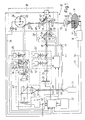
- the latter is designed as a one-channel system, in which only a single laser light bundle, designated overall by 12, is used for exposing the structure to be imprinted on a photoresist layer.
- This laser light bundle 12 is focused by means of a microscope objective 13 on the surface of the photoresist layer of the wafer 11 to be exposed, the focal spot, corresponding to the half-width of the Gaussian intensity profile of the laser light bundle in focus, a typical diameter of approximately 0.25 ⁇ m Has.
- the intensity of the laser light beam 12 can be changed in the ratio 500/1 by means of an acousto-optical modulator 14. If necessary, it can be finely graded.
- the wafer 11 can be moved back and forth in the X and Y coordinate directions marked by the arrows 17 and 18 by means of a wafer transport device 16 which is only indicated schematically, the X and Y transport strokes which can be carried out by means of the wafer transport device being sufficiently large are to the entire wafer surface to be able to expose the laser light beam 12.
- a first optical scanning device designated overall by 19, within the field of view of the microscope objective 13, which has a typical value of 250 m, line deflection of the laser light bundle 12 or the focal spot 21 in the X direction takes place (FIG. 2). possible.
- the wafer 11 is moved along the meandering or by means of the transport device 16.
- the line deflection is achieved by means of a rotatably drivable polygon mirror 26 provided in the arrangement shown in FIG. 1, with the result that the focal spot 21 extends in parallel lines 27 from one edge 28 to the opposite edge 29 of each strip-shaped area 24 emotional.
- the feed speed in the Y direction can be adjusted so that the distance measured in the Y direction between two successively swept scanning lines 27 is approximately equal to half the focal spot diameter, and is therefore 0.125 ⁇ m in the selected explanatory example .
- the acousto-optical modulator 14 provided for the brightness or Canaloscuro control of the laser light beam 12 can be controlled with a 40 MHz signal, i.e. the intensity of the laser light beam can be set to 40 million different values in 1 second. If it is provided that 27 2000 pixels should be exposed per line, which corresponds to a distance of 0.125 ⁇ m in the X direction, 20,000 lines 27 can be exposed point-by-point per second, whose line spacing is also 0.125 ⁇ m, and the result is a dot and line grid equidistant in the X and Y directions for the exposure.
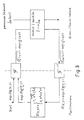
- the structure to be produced by exposure of the respective photoresist layer is stored in a disk memory combined with a computer 31 and can be successively read into the computer as the exposure process progresses and processed by the latter to control the acousto-optical modulator 14 in a suitable manner.
- the computer 31 is through feedback signals received from the wafer transport device 16, which contain the information about the momentary position of the wafers 11, and through feedback signals which contain the information contain about the instantaneous amount of the line deflection and the computer via the signal lines 33 and 34 and the line deflection and feedback line 36, synchronized with the wafer movement or the line scanning movement of the laser light beam 12.
- This second scanning device 38 is operated asynchronously to the first scanning device 19 and at a significantly lower scanning frequency.
- the light reflected from the wafer surface by reflection into the beam path of the second scanning device 38 is detected with a two-dimensional (2d) matrix arrangement of photoelectric receivers, preferably a diode matrix 39, with regard to its two-dimensional spatial intensity distribution, the intensity distribution of each of the illuminated surface elements of the wafers 11 reflected radiation is measured and stored for further processing.
- the point image function detected in this way is performed using known algorithms, the basic features of which will be briefly explained below for a better understanding by the computer 31, a comparison of the measured intensity distribution with a characteristic of accurate focusing of the total of 41 scanning light bundle on the scanned wafer surface - ideal - point image function performed.
- a control signal transmitter 42 connected downstream of the computer 31 is activated, with the output signals of which a so-called active mirror 43, ie a mirror with electrically controllable refractive power, is activated, which is now in the exposure beam path of the laser Lithographs 10 provides a compensatory focus shift in that the exposure laser light bundle 12 is precisely focused on the surface of the photoresist layer to be blasted within narrow tolerances.
- a continuous, automatic readjustment of the focal spot 21 of the exposure laser light beam to the surface of the respective photoresist layer can be achieved in the course of the exposure of a photoresist layer. It goes without saying that this refocusing cannot be carried out for every point to be exposed, but because the computational processing of the point image function takes a certain time, for example only for each of the lines 27 to be exposed.
- the starting point is the plausible assumption that the light field at the location (x, y) of the entrance pupil 44 of the microscope objective 13 has a plane wavefront that can be characterized by a phase factor ⁇ o (x, y).
- ⁇ o phase factor
- the course of the light field is ⁇ I (u, v) . expi ⁇ (u, v) in the focal plane - the surface of the photoresist layer of the microscope objective 13 to be exposed.
- a course of the wave front at the entrance pupil 44 of the microscope objective 17 is consistent with this field course, ie a phase factor ⁇ 1 (x, y ) calculated.
- this phase factor is now used to describe the light field at the location of the entrance pupil applied and again, as described above, the wave field in the focal plane of the microscope objective 17 is calculated; Furthermore, the amplitude factors are replaced by the roots of the measured intensity values and the new phase factor ⁇ 2 (x, y) is calculated.
- the laser beam lithograph 10 explained in this respect on the basis of its basic structure and its essential functions is further characterized by the following structural and functional details:
- the primary beam of the argon laser 37 represented by the dash-dotted central beam 46 and its marginal beams 47 and 48 is essentially a parallel bundle with a bundle cross section of approximately 1 mm 2. It is adjusted by means of a beam shaping and focus adjustment optics, designated in total by 49, which comprises the active mirror 43, to the further use of the laser light Bundle shape brought in the sense of an adaptation of the bundle cross-section to the optical devices available for further optical processing and in the sense of a targeted refocusing, if necessary also a targeted defocusing of the laser light bundle 12 in the region of the photoresist layer to be exposed.
- Targeted defocusing of the laser light beam 12 to enlarge the focal spot 21, which can be controlled by means of the computer 31, can be expedient if relatively wide and large areas are to be exposed uniformly.
- the active mirror is arranged in a pupil plane 44 ′ corresponding to the plane of the entrance pupil 44 of the microscope objective. It is - in the illustrated embodiment - illuminated via a partially transparent, for example semi-transparent, mirror 51, which extends the primary light beam 46, 47, 48 of the argon laser 37 toward the active mirror 43 by means of a telecentric lens arrangement which comprises the two converging lenses 52 and 53 of different focal lengths redirects.
- the light flux reflected by the active mirror 43 is increased by means of a further telecentric arrangement of lenses 54 and 56, in whose common focal plane the acousto-optical intensity modulator 14 is arranged brought the cross section suitable for the further use of the laser luminous flux already explained, with which the laser light bundle represented by the marginal rays 47 'and 48' emerges at the output 57 of the beam shaping optics 49.
- the active mirror 43 its principal Structure shown in Figure 4 is designed as a so-called film mirror. It comprises a grounded and mirrored film 58, which is located between a transparent electrode 59 and an arrangement of separately controllable individual electrodes 61.
- the counter electrode is kept at a constant potential U o . Applying different voltages to the individual electrodes results in electrostatic forces acting on the film 58, which can be used to deliberately deform this film in such a way that the active mirror receives a positive or negative refractive power.
- the output light bundle 47 ', 48' of the beam shaping optics 49 is fed to the first scanning device 19 which, by rotating the polygon mirror 26, mediates the line deflection of the laser light bundle 12 or the focal spot 21 in the X direction. It is also provided with a Y deflection device 62, the use of which will be discussed in more detail below.
- the polygon mirror shown in FIG. 1 with only 8 facets 63, which can be rotated about the axis 64 perpendicular to the plane of the drawing, has 24 facets in a typical polygonal arrangement in a typical embodiment. It can be driven by means of an electric motor 66.
- the Y deflection device 62 additionally provided in the context of the first scanning device 19 is realized in a design known per se by a galvanometer mirror which can be driven pivotably about a horizontal axis 65.
- the facet surfaces 63 of the polygon mirror 26 are shown in FIG a telecentric beam path, which is illustrated by the two lenses 67 and 68, is imaged on the reflecting surface 69 of the galvanometer mirror 62.
- a deflection mirror 71 arranged between the exit lens 68 of this telecentric beam path 67, 68 and the galvanometer mirror 62 is only provided to achieve a favorable beam path geometry.
- the reflecting surface 69 of the galvanometer mirror 72 is imaged on the entrance pupil 44 of the microscope objective 13, which in turn is the laser light bundle 12 which passes through the entrance pupil 44 as a parallel bundle or almost parallel light bundle focused on the surface of the wafer 11 to be exposed.
- first partially transparent mirror 74 usually a semi-transparent mirror, which is arranged between the polygon mirror 26 and the output 57 of the beam shaping optics 49 and is part of one first detection arrangement, designated overall by 76, is coupled out in the direction of arrow 77 from the exposure beam path.
- This decoupled light bundle is focused by means of a further microscope objective 78.
- a pinhole 81 is arranged in the focal plane 79 of this further microscope objective 78, which conveys a bundle limitation in such a way that through this pinhole 81 only such light can strike a photomultiplier 82 that comes from the depth of field of the microscope objective 13 corresponding region of the focusing plane of the exposure beam path.
- connection marks can be "seen” in the reflected UV light, which are provided for a continuous and precise division of the lines 27 of adjacent strip-shaped areas 24 and are each generated in a method step carried out before the exposure of the new photoresist layer and to be precise in narrow overlapping areas of the adjacent surface strips 24 of the wafers 11.
- the desired locations of such identification marks are stored in the computer 31. If the detection signal of the photomultiplier 82 occurs earlier or later in the course of an exposure process than it corresponds to the desired position stored in the computer 31, this is an indication that the lines 27 in the strip 24 of the wafer surface which is subjected to the exposure are opposite the ones Lines of the previously exposed strip are offset.
- the computer 31 then generates a control signal for the Y deflection device 62 of the first scanning device, as a result of which the galvanometer mirror 62 can be adjusted to such an extent that the offset of the lines 27 in the Y direction is compensated for again.
- a second detection device 83 analogous to the first detection device 76 can also be used, which measures the intensity of the UV radiation luminescence radiation induced in a photoresist layer.
- Marks recognizable by means of the second detection device 83 can e.g. be produced by bleaching the photoluminescence in partial areas of the wafer surface.
- the second scanning device 38 comprises, as scanning elements, a first galvanometer mirror 87 which can be pivoted about a horizontal axis 86, ie axis 86 parallel to the plane of propagation of the scanning light, and which mediates the Y deflection of the scanning light, and a second galvanometer mirror 87 which rotates around an axis 88 running perpendicular to the plane of propagation of the scanning light is pivotable and accordingly conveys the X-line deflection.
- first mirror 89 which is transparent to the UV laser light and reflects the wavelength 514 nm
- a deflection mirror 91, a partially transparent mirror 92, the second scanning device 38 and one further partially transparent mirror 93 is coupled into the beam path provided for illuminating the wafer surface, this coupling of the further scanning luminous flux 41 taking place between the galvanometer mirror 62 of the first scanning device 19 and the one lens 72 of the telecentric lens arrangement 72, 73, which in front of the entrance pupil 44 of the microscope objective 17 is arranged.
- the first and second detection devices 76 and 83 are provided with analog, further detection devices 76 'and 83', which likewise enable the detection of connection marks, the position of which in relation to the desired locations stored in the computer 31 now using the reflected scanning light (Detection arrangement 76 ') or, in turn, the detected luminescence radiation (detection device 83') is recognized, as already explained with reference to the detection device 83.
- An exposure frequency of 40 MHz can be achieved with the laser beam lithograph 10 explained with reference to FIG. 40 million picture elements (pixels) of an exposure structure can be generated per second.
- a beam shaping and refocusing optics 49 'shown in FIG. 5 are provided, which have two mirrors 43' and 43 '' which are active in the sense explained above. comprises which in the Z-ray path shown in FIG. 5 between the telecentric lens systems 52, 53 and 54, 56 analog lens system 52 ', 53' and 54 ', 56' are arranged.
- the two active mirrors 43 'and 43'' are designed as facet mirrors, each of which has the same number of spherical facet surfaces 96 and 97, respectively.
- One of the spherical facets 96 of one active mirror 43 ' is conjugated to one of the spherical facets 97 of the other active mirror 43' in such a way that they have a common focus, the central axes 98 of each of one of the facet pairs 96, 97 Z. -form-reflected, convergent light beams run essentially parallel to each other.
- the intensities of the light bundles converging between the two active mirrors 43 'and 43'' can be individually modulated in a computer-controlled manner by means of an arrangement of acousto-optical modulators, designated as 99, which are arranged in the common focal plane of the mirror facets 96 and 97.
- the refractive powers and orientations of the mirror facets 96 and 97 are set by computer-controlled voltage application of the control electrodes of the active mirrors 43 'and 43''in such a way that the functional combination of the beam shaping optics 49' with the other functional elements of the laser beam lithograph 1, on the surface of the wafers 11, a linear or almost linear arrangement of focal spots lying closely next to one another in the Y direction results, the distance of which corresponds, for example, to half the focal spot diameter.
- Beam shaping optics 49 ' is then possible in the manner analogous to that described above for multi-channel operation of the laser lithograph 10, with the result that the working frequency is increased by the factor corresponding to the number of exposure channels.
Landscapes
- Physics & Mathematics (AREA)
- General Physics & Mathematics (AREA)
- Engineering & Computer Science (AREA)
- Power Engineering (AREA)
- Manufacturing & Machinery (AREA)
- Computer Hardware Design (AREA)
- Microelectronics & Electronic Packaging (AREA)
- Optics & Photonics (AREA)
- Condensed Matter Physics & Semiconductors (AREA)
- Exposure And Positioning Against Photoresist Photosensitive Materials (AREA)
- Exposure Of Semiconductors, Excluding Electron Or Ion Beam Exposure (AREA)
- Automatic Focus Adjustment (AREA)
- Mechanical Optical Scanning Systems (AREA)
- Mechanical Light Control Or Optical Switches (AREA)
- Lasers (AREA)
- Semiconductor Lasers (AREA)
- Laser Surgery Devices (AREA)
- Materials For Photolithography (AREA)
Claims (5)
- Presse lithographique à rayon laser pour la fabrication de composants semiconducteurs hautement intégrés dont les éléments fonctionnels sont produits en recouvrant une "galette", ou lame, de couches structurées riches en détails aux propriétés de conductibilité électrique variées, l'enregistrement de la structure de lignes et de surfaces prévue dans une couche s'effectuant par exposition, conforme à cette structure, d'une couche de laque photosensible appliquée sur la surface caractéristique chaque fois de la phase concernée du processus de fabrication, la presse étant équipée d'au moins un canal d'exposition au moyen duquel la surface de la couche de laque photosensible à exposer peut être balayée, les mouvements relatifs de la lame et du rayon éclairant nécessaires à ce balayage s'effectuant tant par déviation de ce rayon que par des déplacements de la lame, commandés par calculateur, dans deux directions de coordonnées orthogonales l'une à l'autre, ainsi que d'un modulateur acoustico-optique (14) pour la modulation en intensité du rayon éclairant, caractérisée en ce que le parcours du rayon éclairant comprend, en tant qu'organe de focalisation, au moins un miroir actif (43 ; 43', 43") à distance focale réglable par voie électrique, en ce qu'il est prévu un équipement explorateur (38) au moyen duquel la répartition dans l'espace d'une lumière d'essai (41) réfléchie sur des éléments de surface judicieusement choisis de la lame (11) peut être décelée, et en ce que dans le cadre du calculateur prévu pour la commande de l'exposition et pour la détection de la répartition de l'intensité de la lumière réfléchie (fonction d'image ponctuelle) il est prévu un comparateur qui à partir de la comparaison de la fonction d'image ponctuelle décelée avec une fonction d'image ponctuelle idéale caractéristique d'une focalisation optimale de la lumière d'essai, c'est-à-dire du flux lumineux éclairant, génère des signaux de commande pour le miroir actif (43, 43', 43") en vue du réglage de conditions de focalisation bien définies.
- Presse lithographique à rayon laser selon la revendication 1, caractérisée en ce qu'il est prévu un équipement de décomposition de rayon (43', 43") qui réalise une décomposition du rayon primaire d'un laser (37), prévu à des fins d'exposition, en un certain nombre de rayons partiels dont les intensités peuvent être variées indépendamment les unes des autres au moyen d'un dispositif modulateur (99), les faisceaux lumineux partiels résultant de la décomposition du rayon primaire pouvant être focalisés individuellement sur la surface à exposer de la lame.
- Presse lithographique à rayon laser selon la revendication 1 ou 2, caractérisée en ce qu'il est prévu une optique de formation de rayon qui réalise une décomposition du rayon primaire de la source lumineuse laser (37), prévue pour l'exposition de la couche de laque photosensible, en un certain nombre de rayons partiels qui peuvent être focalisés individuellement sur la surface à exposer, et dont les intensités peuvent chacune être réglées séparément par un modulateur acoustico-optique.
- Presse lithographique à rayon laser selon la revendication 3, caractérisée en ce qu'une optique de formation de rayon (49') prévue pour la décomposition du rayon primaire de la source lumineuse laser (37) comprend deux miroirs actifs (43' et 43") qui comprennent chacun le même nombre de surfaces formant facettes sphériques (96 et 97) dans une disposition à foyer commun, et en ce qu'un dispositif modulateur, qui comprend un nombre de modulateurs acoustico-optiques correspondant au nombre des paires de facettes conjuguées (96, 97), est disposé dans le plan focal commun des deux miroirs actifs (43' et 43").
- Presse lithographique à rayon laser selon l'une quelconque des revendications précédentes, caractérisée en ce qu'il est prévu au moins un dispositif indicateur photoélectrique (76 ; 83 ; 76' ; 83') au moyen duquel peut être décelée l'intensité de la lumière qui, renvoyée dans le parcours du rayon éclairant ou dans le parcours de rayons explorateurs, a été réfléchie par des points sélectionnés de la surface de la lame ou a été émise par luminescence.
Priority Applications (1)
| Application Number | Priority Date | Filing Date | Title |
|---|---|---|---|
| AT85109357T ATE64236T1 (de) | 1984-07-26 | 1985-07-25 | Laserstrahl-lithograph. |
Applications Claiming Priority (2)
| Application Number | Priority Date | Filing Date | Title |
|---|---|---|---|
| DE3427611A DE3427611A1 (de) | 1984-07-26 | 1984-07-26 | Laserstrahl-lithograph |
| DE3427611 | 1984-07-26 |
Publications (3)
| Publication Number | Publication Date |
|---|---|
| EP0173849A2 EP0173849A2 (fr) | 1986-03-12 |
| EP0173849A3 EP0173849A3 (en) | 1988-06-08 |
| EP0173849B1 true EP0173849B1 (fr) | 1991-06-05 |
Family
ID=6241658
Family Applications (1)
| Application Number | Title | Priority Date | Filing Date |
|---|---|---|---|
| EP85109357A Expired - Lifetime EP0173849B1 (fr) | 1984-07-26 | 1985-07-25 | Lithographie par rayon laser |
Country Status (5)
| Country | Link |
|---|---|
| US (1) | US4727381A (fr) |
| EP (1) | EP0173849B1 (fr) |
| JP (1) | JPS61116360A (fr) |
| AT (1) | ATE64236T1 (fr) |
| DE (2) | DE3427611A1 (fr) |
Cited By (1)
| Publication number | Priority date | Publication date | Assignee | Title |
|---|---|---|---|---|
| DE10358415A1 (de) * | 2003-12-13 | 2005-07-07 | Lambertus Monnee | Computergesteuertes Verfahren zur Darstellung der Bewegungsbahn eines Werkzeuges zur Ausbeulung einer Delle in einem Karosserieblech durch einen laufenden Lichtpunkt |
Families Citing this family (45)
| Publication number | Priority date | Publication date | Assignee | Title |
|---|---|---|---|---|
| JPS62279627A (ja) * | 1986-05-28 | 1987-12-04 | Toshiba Mach Co Ltd | ビ−ム描画装置の描画方法 |
| CH670592A5 (fr) * | 1986-09-22 | 1989-06-30 | Lasarray Holding Ag | |
| NL8700612A (nl) * | 1987-03-13 | 1988-10-03 | Tno | Confocale laserscanning microscoop. |
| FR2621762B1 (fr) * | 1987-10-09 | 1994-06-17 | Thomson Csf | Procede et dispositif pour l'inscription d'image par laser, et dispositif obtenu par ce procede |
| US4901718A (en) * | 1988-02-02 | 1990-02-20 | Intelligent Surgical Lasers | 3-Dimensional laser beam guidance system |
| US4912487A (en) * | 1988-03-25 | 1990-03-27 | Texas Instruments Incorporated | Laser scanner using focusing acousto-optic device |
| US5592211A (en) * | 1988-03-25 | 1997-01-07 | Texas Instruments Incorporated | Laser pattern/inspector with a linearly ramped chirp deflector |
| US4947039A (en) * | 1988-10-17 | 1990-08-07 | Eotron Corporation | Flat stationary field light beam scanning device |
| US5327338A (en) * | 1990-01-31 | 1994-07-05 | Etec Systems, Inc. | Scanning laser lithography system alignment apparatus |
| US5124927A (en) * | 1990-03-02 | 1992-06-23 | International Business Machines Corp. | Latent-image control of lithography tools |
| WO1992010049A1 (fr) * | 1990-11-21 | 1992-06-11 | Polaroid Corporation | Systeme d'impression optique avec support d'impression discontinu |
| US5274397A (en) * | 1991-05-14 | 1993-12-28 | Firstech Properties Company | Large-format plotter using segmented raster-scanning |
| US5619488A (en) * | 1991-09-07 | 1997-04-08 | Fuji Xerox Co., Ltd. | Information recording device |
| US5331338A (en) * | 1992-01-30 | 1994-07-19 | Printware, Inc. | Web steering for an image recorder |
| US5246435A (en) * | 1992-02-25 | 1993-09-21 | Intelligent Surgical Lasers | Method for removing cataractous material |
| EP0558781B1 (fr) * | 1992-03-05 | 1998-08-05 | Micronic Laser Systems Ab | Méthode et dispositif pour l'exposition de substrats |
| US5656186A (en) * | 1994-04-08 | 1997-08-12 | The Regents Of The University Of Michigan | Method for controlling configuration of laser induced breakdown and ablation |
| US5633672A (en) * | 1994-09-13 | 1997-05-27 | Eastman Kodak Company | Real-time calibration of processless writer |
| DE19511119A1 (de) * | 1995-03-20 | 1995-10-05 | Frenck H J Dr | Verfahren und Vorrichtung zur Präparation von Strukturen in dünnen Schichten durch Direktbeleuchtung einer fotoempfindlichen Schicht |
| JP3591922B2 (ja) * | 1995-07-17 | 2004-11-24 | キヤノン株式会社 | 光量測定装置 |
| US6246706B1 (en) | 1999-05-27 | 2001-06-12 | Spectra Physics Lasers, Inc. | Laser writing method and apparatus |
| DE19957418B4 (de) * | 1999-11-29 | 2016-02-04 | Leica Microsystems Cms Gmbh | Verfahren zur lichtoptischen Abtastung eines Objekts und Rastermikroskop zur Anwendung des Verfahrens |
| US6324191B1 (en) | 2000-01-12 | 2001-11-27 | Intralase Corp. | Oscillator with mode control |
| US6341009B1 (en) | 2000-02-24 | 2002-01-22 | Quantronix Corporation | Laser delivery system and method for photolithographic mask repair |
| US8497450B2 (en) * | 2001-02-16 | 2013-07-30 | Electro Scientific Industries, Inc. | On-the fly laser beam path dithering for enhancing throughput |
| US20020170887A1 (en) * | 2001-03-01 | 2002-11-21 | Konica Corporation | Optical element producing method, base material drawing method and base material drawing apparatus |
| US7843632B2 (en) * | 2006-08-16 | 2010-11-30 | Cymer, Inc. | EUV optics |
| US6610050B2 (en) | 2001-07-27 | 2003-08-26 | 20/10 Perfect Vision, Optische Geraete Gmbh | Laser beam delivery system with multiple focal points |
| EP1446703A2 (fr) | 2001-11-07 | 2004-08-18 | Applied Materials, Inc. | Imprimante a matrice en grille de points optique |
| JP2005533365A (ja) | 2001-11-07 | 2005-11-04 | アプライド マテリアルズ インコーポレイテッド | マスクレスの光子−電子スポット格子アレイ印刷装置 |
| US7618415B2 (en) * | 2004-04-09 | 2009-11-17 | Technolas Perfect Vision Gmbh | Beam steering system for corneal laser surgery |
| US7633034B2 (en) * | 2004-06-18 | 2009-12-15 | Electro Scientific Industries, Inc. | Semiconductor structure processing using multiple laser beam spots overlapping lengthwise on a structure |
| US8148211B2 (en) * | 2004-06-18 | 2012-04-03 | Electro Scientific Industries, Inc. | Semiconductor structure processing using multiple laser beam spots spaced on-axis delivered simultaneously |
| US7629234B2 (en) * | 2004-06-18 | 2009-12-08 | Electro Scientific Industries, Inc. | Semiconductor structure processing using multiple laterally spaced laser beam spots with joint velocity profiling |
| US7687740B2 (en) * | 2004-06-18 | 2010-03-30 | Electro Scientific Industries, Inc. | Semiconductor structure processing using multiple laterally spaced laser beam spots delivering multiple blows |
| US7435927B2 (en) | 2004-06-18 | 2008-10-14 | Electron Scientific Industries, Inc. | Semiconductor link processing using multiple laterally spaced laser beam spots with on-axis offset |
| US7935941B2 (en) * | 2004-06-18 | 2011-05-03 | Electro Scientific Industries, Inc. | Semiconductor structure processing using multiple laser beam spots spaced on-axis on non-adjacent structures |
| US8110775B2 (en) * | 2004-06-18 | 2012-02-07 | Electro Scientific Industries, Inc. | Systems and methods for distinguishing reflections of multiple laser beams for calibration for semiconductor structure processing |
| US8383982B2 (en) * | 2004-06-18 | 2013-02-26 | Electro Scientific Industries, Inc. | Methods and systems for semiconductor structure processing using multiple laser beam spots |
| US7923306B2 (en) * | 2004-06-18 | 2011-04-12 | Electro Scientific Industries, Inc. | Semiconductor structure processing using multiple laser beam spots |
| US7371596B2 (en) * | 2004-12-30 | 2008-05-13 | Semicube, Inc. | Parallel-beam scanning for surface patterning of materials |
| US20070173796A1 (en) * | 2006-01-25 | 2007-07-26 | Ralf Kessler | Device and method for calibrating a laser system |
| US7643521B2 (en) * | 2006-07-27 | 2010-01-05 | Technolas Perfect Vision Gmbh | Material processing system with variable repetition rate laser |
| JP2013138100A (ja) * | 2011-12-28 | 2013-07-11 | Dainippon Screen Mfg Co Ltd | 描画装置および描画方法 |
| DE102012000650A1 (de) * | 2012-01-16 | 2013-07-18 | Carl Zeiss Microscopy Gmbh | Verfahren und vorrichtung zum abrastern einer oberfläche eines objekts mit einem teilchenstrahl |
Family Cites Families (6)
| Publication number | Priority date | Publication date | Assignee | Title |
|---|---|---|---|---|
| DE2012394A1 (de) * | 1970-03-16 | 1971-10-14 | Siemens Ag | Anordnung zur direkten und abschnittsweisen Belichtung von lichtempfindlichen Schichten |
| US4001840A (en) * | 1974-10-07 | 1977-01-04 | Precision Instrument Co. | Non-photographic, digital laser image recording |
| JPS54128303A (en) * | 1978-03-29 | 1979-10-04 | Victor Co Of Japan Ltd | Optical reproducing device of information recording medium disc |
| JPS5567722A (en) * | 1978-11-16 | 1980-05-22 | Fuji Photo Film Co Ltd | Light beam recorder |
| JPS57102016A (en) * | 1980-12-17 | 1982-06-24 | Hitachi Ltd | Pattern generator |
| US4541712A (en) * | 1981-12-21 | 1985-09-17 | Tre Semiconductor Equipment Corporation | Laser pattern generating system |
-
1984
- 1984-07-26 DE DE3427611A patent/DE3427611A1/de not_active Withdrawn
-
1985
- 1985-07-23 US US06/758,061 patent/US4727381A/en not_active Expired - Fee Related
- 1985-07-25 EP EP85109357A patent/EP0173849B1/fr not_active Expired - Lifetime
- 1985-07-25 AT AT85109357T patent/ATE64236T1/de not_active IP Right Cessation
- 1985-07-25 DE DE8585109357T patent/DE3583087D1/de not_active Expired - Lifetime
- 1985-07-26 JP JP60164211A patent/JPS61116360A/ja active Granted
Cited By (2)
| Publication number | Priority date | Publication date | Assignee | Title |
|---|---|---|---|---|
| DE10358415A1 (de) * | 2003-12-13 | 2005-07-07 | Lambertus Monnee | Computergesteuertes Verfahren zur Darstellung der Bewegungsbahn eines Werkzeuges zur Ausbeulung einer Delle in einem Karosserieblech durch einen laufenden Lichtpunkt |
| DE10358415B4 (de) * | 2003-12-13 | 2007-02-15 | Lambertus Monnee | Computergesteuertes Verfahren zur Darstellung der Bewegungsbahn eines Werkzeuges zur Ausbeulung einer Delle in einem Karosserieblech durch einen laufenden Lichtpunkt |
Also Published As
| Publication number | Publication date |
|---|---|
| EP0173849A3 (en) | 1988-06-08 |
| JPS61116360A (ja) | 1986-06-03 |
| ATE64236T1 (de) | 1991-06-15 |
| EP0173849A2 (fr) | 1986-03-12 |
| DE3427611A1 (de) | 1988-06-09 |
| JPH0513368B2 (fr) | 1993-02-22 |
| US4727381A (en) | 1988-02-23 |
| DE3583087D1 (en) | 1991-07-11 |
Similar Documents
| Publication | Publication Date | Title |
|---|---|---|
| EP0173849B1 (fr) | Lithographie par rayon laser | |
| EP0168643B1 (fr) | Dispositif pour l'inspection de pastilles de semi-conducteurs | |
| DE3137031C2 (de) | Mehrfachstrahlenbündel-Abtastoptiksystem | |
| EP1168813B1 (fr) | Source laser d'illumination à plusieurs faisceaux et procédé d'entrelacement de lignes de balayage à trame pour l'exposition de plaques d'impression | |
| DE19827423C2 (de) | Zweidimensionale Laserdiodenanordnung | |
| DE102011112649B4 (de) | Laserspotsteuerung in MALDI-Massenspektrometern | |
| WO1998000760A1 (fr) | Dispositif d'exposition pour lithographie et procede de lithographie | |
| DE69724331T2 (de) | Verfahren zur Herstellung eines Düsenkörpers und Arbeitsgerät | |
| DE3933308A1 (de) | Abtast- und wiederholungs-projektionslithographiesystem mit hoher aufloesung | |
| EP0898783A2 (fr) | Microscope a balayage dans lequel un echantillon est excite optiquement simultanement en plusieurs points | |
| DE19503675A1 (de) | Optisches Übertragungssystem und Verfahren zur Lichtausstrahlung | |
| DE3806785A1 (de) | Optischer drucker | |
| DE2758305C2 (de) | Verfahren und Vorrichtung zur Vermeidung von Zeilenstrukturen bei der Bildaufzeichnung | |
| DE4313111A1 (de) | Verfahren zur Herstellung einer druckenden Vorlage, insbesondere einer Druckform einer Druckmaschine | |
| DE3139106A1 (de) | Integrierte wellenleiter-tropfensensoranordnung fuer ein farbtroepfchenstrahl-drucksystem | |
| DE2411508C2 (de) | Vorrichtung zum Erzeugen von Masken für Mikroschaltkreise | |
| DE102007038704B4 (de) | Substratbelichtungsvorrichtung | |
| DE10058761B4 (de) | Abbildungsvorrichtung | |
| EP0184063B1 (fr) | Méthode de positionnement de formes d'impression avant le poinçonnage des trous de positionnement ainsi que dispositif pour la mise en oeuvre du procédé | |
| DE10013299A1 (de) | Verfahren und Vorrichtung zur geometrischen Kalibrierung pixelorientierter photosensitiver Elemente | |
| DE4127919C2 (de) | Lichtaufzeichnungsvorrichtung | |
| DE19955107B4 (de) | Thermisches Aufzeichnen mit variabler Energiedichte | |
| DE3624163C2 (de) | Gerät zur Erzeugung eines Musters auf einem eine strahlungsempfindliche Schicht aufweisenden Werkstück | |
| DE2742264B2 (de) | Verfahren zur Abbildung eines Objektes mit geringer Vergrößerung mittels eines Korpuskularstrahlgeräts, insbesondere eines Elektronen-Mikroskops und Korpuskularstrahlgerät zur Durchführung des Verfahrens | |
| EP2356518B1 (fr) | Procede et dispositif d'imagerie d'un substrat sensible au rayonnement |
Legal Events
| Date | Code | Title | Description |
|---|---|---|---|
| PUAI | Public reference made under article 153(3) epc to a published international application that has entered the european phase |
Free format text: ORIGINAL CODE: 0009012 |
|
| AK | Designated contracting states |
Kind code of ref document: A2 Designated state(s): AT CH DE FR GB IT LI NL |
|
| PUAL | Search report despatched |
Free format text: ORIGINAL CODE: 0009013 |
|
| AK | Designated contracting states |
Kind code of ref document: A3 Designated state(s): AT CH DE FR GB IT LI NL |
|
| 17P | Request for examination filed |
Effective date: 19880723 |
|
| RAP1 | Party data changed (applicant data changed or rights of an application transferred) |
Owner name: HEIDELBERG INSTRUMENTS GMBH |
|
| RIN1 | Information on inventor provided before grant (corrected) |
Inventor name: HUNKLINGER, SIEGFRIED, PROF. DR. Inventor name: BILLE, JOSEF, PROF. DR. |
|
| 17Q | First examination report despatched |
Effective date: 19900905 |
|
| GRAA | (expected) grant |
Free format text: ORIGINAL CODE: 0009210 |
|
| AK | Designated contracting states |
Kind code of ref document: B1 Designated state(s): AT CH DE FR GB IT LI NL |
|
| PG25 | Lapsed in a contracting state [announced via postgrant information from national office to epo] |
Ref country code: NL Effective date: 19910605 Ref country code: IT Free format text: LAPSE BECAUSE OF FAILURE TO SUBMIT A TRANSLATION OF THE DESCRIPTION OR TO PAY THE FEE WITHIN THE PRESCRIBED TIME-LIMIT;WARNING: LAPSES OF ITALIAN PATENTS WITH EFFECTIVE DATE BEFORE 2007 MAY HAVE OCCURRED AT ANY TIME BEFORE 2007. THE CORRECT EFFECTIVE DATE MAY BE DIFFERENT FROM THE ONE RECORDED. Effective date: 19910605 Ref country code: FR Effective date: 19910605 |
|
| REF | Corresponds to: |
Ref document number: 64236 Country of ref document: AT Date of ref document: 19910615 Kind code of ref document: T |
|
| REF | Corresponds to: |
Ref document number: 3583087 Country of ref document: DE Date of ref document: 19910711 |
|
| PG25 | Lapsed in a contracting state [announced via postgrant information from national office to epo] |
Ref country code: AT Effective date: 19910725 |
|
| PG25 | Lapsed in a contracting state [announced via postgrant information from national office to epo] |
Ref country code: LI Effective date: 19910731 Ref country code: CH Effective date: 19910731 |
|
| GBT | Gb: translation of ep patent filed (gb section 77(6)(a)/1977) | ||
| EN | Fr: translation not filed | ||
| NLV1 | Nl: lapsed or annulled due to failure to fulfill the requirements of art. 29p and 29m of the patents act | ||
| GBT | Gb: translation of ep patent filed (gb section 77(6)(a)/1977) | ||
| REG | Reference to a national code |
Ref country code: CH Ref legal event code: PL |
|
| PLBE | No opposition filed within time limit |
Free format text: ORIGINAL CODE: 0009261 |
|
| STAA | Information on the status of an ep patent application or granted ep patent |
Free format text: STATUS: NO OPPOSITION FILED WITHIN TIME LIMIT |
|
| 26N | No opposition filed | ||
| PGFP | Annual fee paid to national office [announced via postgrant information from national office to epo] |
Ref country code: GB Payment date: 19930615 Year of fee payment: 9 |
|
| PGFP | Annual fee paid to national office [announced via postgrant information from national office to epo] |
Ref country code: DE Payment date: 19930729 Year of fee payment: 9 |
|
| PG25 | Lapsed in a contracting state [announced via postgrant information from national office to epo] |
Ref country code: GB Effective date: 19940725 |
|
| GBPC | Gb: european patent ceased through non-payment of renewal fee |
Effective date: 19940725 |
|
| PG25 | Lapsed in a contracting state [announced via postgrant information from national office to epo] |
Ref country code: DE Effective date: 19950401 |