EP0147112A2 - Piezoelektrische Antriebsvorrichtung mit einem bilaminaren Element - Google Patents
Piezoelektrische Antriebsvorrichtung mit einem bilaminaren Element Download PDFInfo
- Publication number
- EP0147112A2 EP0147112A2 EP84308513A EP84308513A EP0147112A2 EP 0147112 A2 EP0147112 A2 EP 0147112A2 EP 84308513 A EP84308513 A EP 84308513A EP 84308513 A EP84308513 A EP 84308513A EP 0147112 A2 EP0147112 A2 EP 0147112A2
- Authority
- EP
- European Patent Office
- Prior art keywords
- voltage
- bimorph element
- circuit
- coin
- actuator according
- Prior art date
- Legal status (The legal status is an assumption and is not a legal conclusion. Google has not performed a legal analysis and makes no representation as to the accuracy of the status listed.)
- Granted
Links
Images


Classifications
-
- H—ELECTRICITY
- H10—SEMICONDUCTOR DEVICES; ELECTRIC SOLID-STATE DEVICES NOT OTHERWISE PROVIDED FOR
- H10N—ELECTRIC SOLID-STATE DEVICES NOT OTHERWISE PROVIDED FOR
- H10N30/00—Piezoelectric or electrostrictive devices
- H10N30/80—Constructional details
- H10N30/802—Circuitry or processes for operating piezoelectric or electrostrictive devices not otherwise provided for, e.g. drive circuits
-
- H—ELECTRICITY
- H10—SEMICONDUCTOR DEVICES; ELECTRIC SOLID-STATE DEVICES NOT OTHERWISE PROVIDED FOR
- H10N—ELECTRIC SOLID-STATE DEVICES NOT OTHERWISE PROVIDED FOR
- H10N30/00—Piezoelectric or electrostrictive devices
- H10N30/20—Piezoelectric or electrostrictive devices with electrical input and mechanical output, e.g. functioning as actuators or vibrators
- H10N30/204—Piezoelectric or electrostrictive devices with electrical input and mechanical output, e.g. functioning as actuators or vibrators using bending displacement, e.g. unimorph, bimorph or multimorph cantilever or membrane benders
- H10N30/2041—Beam type
- H10N30/2042—Cantilevers, i.e. having one fixed end
-
- H—ELECTRICITY
- H10—SEMICONDUCTOR DEVICES; ELECTRIC SOLID-STATE DEVICES NOT OTHERWISE PROVIDED FOR
- H10N—ELECTRIC SOLID-STATE DEVICES NOT OTHERWISE PROVIDED FOR
- H10N30/00—Piezoelectric or electrostrictive devices
- H10N30/80—Constructional details
- H10N30/87—Electrodes or interconnections, e.g. leads or terminals
Definitions
- the present invention relates to a bimorph element and, more particularly, to a piezoelectric actuator using a unidirectional polarization type bimorph element.
- a compact, thin, low-power drive component may comprise a known PZT (trade name) bimorph element available from Krebeit Inc.
- PZT trade name
- a conventional PZT bimorph element provides only a small displacement and a small force.
- a power of up to 10 mW is required to hold a switching state of a driver so as to keep the bimorph element displaced at one side upon application of a voltage thereto.
- this bimorph element has a large hysteresis and a low resistance to mechanical impact and cannot be used in the coin processing apparatus.
- two piezoceramic elements i.e., piezoelectric plates which consist of lead zirconate-titanate and which are polarized along the direction of thickness thereof are overlapped.
- One end of each of the piezoceramic elements is fixed.
- a voltage having the same polarity as the polarization of the piezoceramic elements is applied to one piezoceramic element, and a voltage having a polarity opposite to the polarization of the piezoceramic elements is applied to the other piezoceramic element.
- an electric field acting along the direction of thickness is applied to the respective piezoceramic elements which are displaced along opposing directions in accordance with a piezoelectric transverse displacement effect, thereby flexing the free end portions thereof.
- Conventional bimorph elements are classified into a parallel type element wherein the overlapping piezoceramic elements are polarized in one direction with respect to the direction of thickness thereof, and a / series type wherein the overlapping piezoceramic elements are polarized'in opposing directions with respect to the direction of thickness thereof.
- the parallel type element can provide a large displacement at a low voltage and can be used in place of the electromagnet.
- a voltage is applied to one piezoceramic element in the same direction as the polarization of the elements, and another voltage is applied to the other piezoceramic element in a direction opposite to the polarization, thereby displacing the free ends along a given direction. Thereafter, the polarities of the applied voltages are switched to restore the initial polarization states of the piezoceramic elements.
- the above operation must be repeated, in the piezoceramic element with the applied voltage having a polarity opposite to its polarization direction, the polarization effect becomes weakened. Since a piezoelectric actuator must provide a maximum displacement, a power source voltage must be increased.
- a bimorph element comprises two piezoceramic elements each of which has a thickness of about 0.15 mm and whose material has a field strength-of 580 V/mm
- the power source voltage increases to about 80 V to 85 V
- the polarization of the piezoceramic elements is disturbed, and the resultant displacement becomes very small.
- a practical applied voltage is limited to 1/2 to 1/3 of the polarization breakdown voltage.
- a displacement of about 1 mm in a bimorph element having a length of 45 mm is obtained at a voltage of 30 V. In this manner, when a conventional drive circuit is used although the parallel type element is used, a large displacement cannot be obtained since the power source voltage is limited.
- a polarity switching circuit must have electrical characteristics wherein a high voltage can be switched, a switched state can be held at a low power, and carriers charged by the bimorph element at the time of switching can be immediately discharged.
- none of the conventional switching circuits can satisfy these electrical characteristics.
- a.principal object of the present invention to provide a piezoelectric actuator using a bimorph element wherein a large displacement can be obtained with a large force at a low power without depolarizing piezoceramic elements of the bimorph element.
- a piezoelectric actuator using a bimorph element comprising:
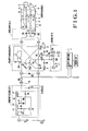
- F ig. 1 shows a piezoelectric actuator using a bimorph element according to an embodiment of the present invention.
- this piezoelectric -actuator basically comprises a parallel type bimorph element 1, a drive input circuit 2, a polarity switching circuit 3, a constant voltage circuit 4, a control circuit 5 and a DC power source E C .
- the bimorph element 1 is connected to the DC power source E C through the drive input circuit 2, the polarity switching circuit 3 and the constant voltage circuit 4.
- the bimorph element 1 includes a pair of piezoceramic elements H1 and H2. These piezoceramic elements H1 and H2 sandwich a central electrode S and are arranged such that their polarization directions are the same (upper-to-lower direction of thickness in Fig.
- Electrodes T1 and T2 are formed on surfaces of the piezoceramic elements Hl and H2 which oppose the inner surfaces thereof contacting the central electrode S.
- One end of the electrode T2 formed on the piezoceramic element H2 is connected to a base.
- the drive input circuit 2 comprises: a Zener diode ZD1, i.e., a constant voltage diode, a cathode of which is connected to the electrode T1 of the piezoceramic element H1; a Zener diode ZD2, an anode of which is connected to the electrode T2 of the piezoceramic element H2; a resistor R1 of a high resistance connected between the electrode T1 and the middle electrode S; and a resistor R 2 of a high resistance connected between the central electrode S and the electrode T2.
- the remaining terminals of the Zener diodes ZD1 and ZD2 are commonly connected, and a common junction point is connected to a terminal A.
- a junction point i.e., the central electrode 5
- the resistors Rl and R2 may be omitted, as indicated by dotted lines.
- the polarity switching circuit 3 comprises: a Darlington-connected pnp transistor pair DTrl, an output of which is connected between the terminal A and a terminal C'; a Darlington-connected pnp transistor pair DTr2, an output of which is connected between the terminal B and the terminal C l ; an NPN transistor TR2, an output of which is connected between the terminal B and a terminal G'; and an NPN transistor Tr4 an output of which is connected between the terminal B and the terminal G'. These transistors are bridged as a polarity switch.
- the input electrode (base) of the transistor pair DTrl is connected to the collector of an NPN transistor Tr7 through a resistor R3.
- the emitter of the NPN transistor Tr7 is grounded.
- the base of the transistor Tr7 is connected to an output terminal of an inverter INV through a resistor R4.
- the emitter of the transistor Tr2 is connected to the output terminal of the inverter INV through a resistor R5.
- the input electrode (base) of the transistor pair DTr2 is connected to the collector of an NPN transistor Tr6 through a resistor R7.
- the emitter of the NPN transistor Tr6 is grounded.
- the base of the transistor Tr6 is connected to the input terminal of the inverter INV through a resistor R8 and to the control circuit 5.
- the base of the transistor Tr4 is also connected to the input terminal of the inverter INV through a resistor R9.
- the control circuit 5 causes a combination of the transistor pair DTrl and the transistor Tr2 and a combination of the transistor pair DTr2 and the transistor Tr4 in the polarity switching circuit 3 to be alternately switched to control polarity switching of the voltage applied to the bimorph element 1.
- the control circuit 5 comprises a resistor R10, a switch SW1 and a DC power source E C .
- the input terminal of the inverter INV is grounded through a resistor R10. At the same time, this input terminal is connected to the positive terminal of the DC power source E C through a slider of the switch SW1 or is grounded.
- the constant voltage circuit 4 comprises: a self-excited ringing choke DC/DC converter using a PNP transistor.
- the constant voltage circuit 4 comprises a saturating transformer TR having coils l - 1, l2 and l3 which are wound in the same direction; a capacitor CB and an electrolytic capacitor C1; resistors RB and RS, a PNP transistor Q1, a diode D1 and a Zener diode ZD3.
- the transistor Q1 together with one end of the coil l2 is connected to a positive terminal F of the DC power source E C .
- the collector of the transistor Q1 is connected to one terminal of the coil l1.
- the other terminal of the coil l2 and one terminal of the coil l3 are commonly connected, and this common junction point is connected to the base of the transistor Q1 through a parallel circuit of the capacitor CB and the resistor RB.
- the base of the transistor Ql is also connected to the other terminal of the coil 11 through the start resistor RS.and to a ground terminal G.
- the base of the transistor Q1 is further connected to the anode of the Zener diode ZD3.
- the cathode of the Zener diode ZD3 is connected to an output terminal C.
- the capacitor Cl is connected between the output terminal C and the ground terminal G.
- the cathode of a diode Dl is connected to the cathode of the Zener diode ZD3.
- the anode of the diode D1 is connected to the other terminal of the coil k3.
- the DC power source E C generates a voltage of, for example, 5 V.
- the relationships between V C' V ZD1 and V ZD2 are given as follows:
- the polarization degradation voltage is defined as a voltage at which the piezoceramic element is depolarized when a voltage having a polarity opposite to the polarization of the piezoceramic element is gradually increased.
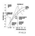
- the polarization degradation voltage will be further clarified with reference to Fig. 2.
- a polarization breakdown voltage Vp In a conventional parallel type piezoelectric element, an AC power source is connected between the opposing electrodes which are commonly connected to the central electrode of the bimorph element, and a displacement ⁇ is measured when the AC voltage E (+E.to -E) is gradually increased to displace the bimorph element. As indicated by a dotted line in Fig. 2, the displacement is increased in accordance with an increase in voltage. However, when a voltage level exceeds a predetermined level, the displacement is abruptly decreased, as previously described. This is because the polarization of the piezoceramic element is broken down upon application of an excessive voltage having a polarity opposite to the polarization of the piezoceramic element. The voltage subjected to polarization breakdown is termed a polarization breakdown voltage Vp.
- the polarization degradation voltage Vd is 1/2 to 1/3 of the breakdown voltage Vp of the piezoceramic element of the PZT system. Referring to Fig. 2, since the polarization breakdown voltage is 80 to 85 V, the polarization degradation voltage Vd becomes about 27 to 40 V.
- the operation of the constant voltage circuit 4 in Fig. 1 will be described.
- a voltage i.e., 5 V
- a current flows through the start resistor in the constant voltage circuit 4, so that the transistor Q1 is turned on.
- a collector current from the transistor Q1 flows through the coil l1 in the transformer Tl
- an induction voltage is generated through the coils l2 and l3, as shown in Fig. 1, so that a current flows through the base circuit consisting of the resistor RB and the capacitor CB.
- the ON state of the transistor Q1 is stabilized, and a larger collector current flows out therefrom.
- the collector current i.e., a current flowing through the coil l1 becomes small, and induction voltages at the coils l2 and l3 are inverted.
- the voltage at the coil l3 is applied to the capacitor C1 which is then charged.
- the magnetic fluxes of the coils l2 and l3 are decreased, and the inverted induction voltages become low.
- a current flows through the coil l2 again from the power source E C to the base circuit consisting of the resistor RB and the capacitor CB serving for the transistor Q1.
- the transistor Q1 is turned on, and the coils l1, l2 and l3 are again excited. In this manner, the transformer TR is self-excited, and carriers are charged in the capacitor C1.
- the Zener diode ZD3 is turned on, and a current will not flow in the base circuit consisting of the resistor RB and the capacitor CB, thereby stopping oscillation.
- oscillation is restarted, thereby obtaining a voltage of E C + V ZD3 .
- the voltage from the power source E C is boosted to obtain the constant voltage V C .
- the control circuit causes the switch SW1 to set in the position as illustrated in Fig. 1, the output from the inverter INV becomes the same as the voltage from the power source E C .
- the transistor Tr2 and then the transistor Tr7 are turned on, so that the Darlington transistor pair DTrl is turned on.
- the voltage V c appears across the terminals A and B.
- each piezoceramic element can be regarded as a capacitor C PZ of 0.01 to several microfarads.
- the reverse bias voltage of the Zener diode is not more than V ZD and the Zener diode is thus kept in the OFF state. In this state, the Zener diode can be regarded as a capacitor C ZD(OFF) of several tens of picofarads to several hundreds of picofarads.
- the Zener diode is regarded as a conductor. For this reason, when a constant voltage V c is applied to a series circuit of the piezoceramic element and the Zener diode through a resistor or a constant current diode CRD, condition C PZ » C ZD(OFF) is established when a charge current starts to flow. Therefore, most of the voltage applied to the series circuit of the piezoceramic element and the Zener diode is applied to the Zener diode. When a voltage at the series circuit has reached the voltage V ZD , the Zener diode is turned on.
- the piezoceramic element is charged with a voltage V C - V ZP .
- the reverse-biased OFF capacitance of the constant voltage circuit used in the present invention must be smaller than the capacitance of the piezoceramic element.
- a voltage V C - V ZD1 is applied to the piezoceramic element H1 along a direction opposite to the polarization direction since the Zener diode ZD1 is reverse biased.
- the distal end of the bimorph element 1 is greatly moved downward.
- the switch SW1 By operating the switch SW1 in the manner described above, the distal end of the bimorph element 1 vertically vibrates.
- a displacement of the bimorph element 1 is represented by the solid line in Fig. 2 when the voltages V C - V ZD1,2 are kept constant and the voltage V changes.
- curves a and b represent the displacements when the clamp voltages having a polarity opposite to the polarization direction are 40 V and 30 V, respectively. In this case, the oscillation frequency was 2 Hz..
- the displacement is doubly increased.
- the displacement can be tripled at a voltage of 90 to 100 V. This voltage range can be used in practice.
- the force can be increased at the same rates as described above, so that the a product of the displacement and the generated force in the actuator is improved 4 to 6 times.
- One of the main features of the present invention lies in the fact that a constant voltage V higher than the polarization degradation voltage Vd is applied in the same direction as the polarization direction of the piezoceramic element to recover depolarization caused by application of a voltage in a direction opposite to the polarization direction, thereby preventing degradation of the polarization of the bimorph element.
- This recovery effect (utilization of an increase in polarization) is not conventionally known well.
- Predetermined voltages are respectively applied to piezoceramic elements which constitute parallel bimorph elements in a direction opposite to the polarization direction of the piezoceramic elements.
- each piezoceramic element has a polarization breakdown voltage Vp of about 85 V and a polarization degradation voltage Vd of about 30 V.
- Vp polarization breakdown voltage
- Vd polarization degradation voltage
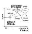
- a time required for attenuating the vibrations of each bimorph element by a predetermined value is shortened by about Vp/10, as indicated by an intersection between the corresponding solid curves and the alternate long and short dashed line, every time the voltage applied to each piezoceramic element in the direction opposite to its polarization direction increases from the polarization degradation voltage Vd by about 1/10.
- the recovery effect obtained by an increase in polarization upon application of a voltage higher than the voltage Vd to the depolarized piezoceramic element in the same direction as the polarization direction for a predetermined period is represented by dotted curves.
- polarization is attenuated by 50% upon application of a voltage Vd + 3Vp/10 ( I - 57 V) for a predetermined period of time, it takes about 10 times the original period of time to recover its polarization when the same voltage is applied in the same direction as its polarization direction.
- V voltage must be higher than the voltage applied in the direction opposite to the polarization direction by Vp/10.
- Inequalities (1) and (2) can be applied to this case. However, even if inequalities (1) and (2) are satisfied, the voltage applied in the direction opposite to the polarization direction is limited. When this voltage comes closer to the voltage Vp, depolarization is abruptly increased, as shown in Fig. 4A. Therefore, even if the polarization effect is obtained, the element has unstable characteristics. In practice, inequality (3) must also be satisfied.
- the driving method for positively utilizing the polarization effect is very effective when a voltage higher than the voltage Vd is applied while the polarities of such a voltage are switched.
- a conventional analog AC power source is used, application of a sufficient voltage to recover the depolarization effect cannot be guaranteed.
- the voltages Vp and Vd greatly depend on changes in temperatures.
- the voltages Vp and Vd must be defined at a given operation temperature.
- the voltages Vp and Vd have negative temperature coefficients and can decrease at high temperatures.
- the voltages Vp and Vd are preferably defined at the upper limit of the operating temperature.
- Fig. 4B is another graph for explaining the effect of the present invention.
- Fig. 4B shows a case wherein the bimorph element in Fig. 4A is operated for a long period of time at a voltage V c of 80 V and a duty of 1/2. Even if a voltage (V C - V ZD ) applied in the direction .. opposite to the polarization direction becomes higher than the polarization degradation voltage Vd and becomes a voltage of 40 to.50 V, degradation does not substantially occur.
- the base current In order to operate one of the Darlington transistor pairs DTrl and DTr2 so as to switch the polarity of the voltage, the base current must be flowed from the constant voltage circuit 4. However,. since the voltage is high, even a small current causes high power consumption.
- the bimorph element serves as a capacitive load, so power is not required to maintain the displacement. However, when the polarity switching circuit 3 greatly consumes power so as to hold the switching state, the bimorph loses its advantage as a low-power element.
- the Darlington transistor pairs DTrl and DTr2 are used to increase the current-amplification factor.
- the current flowed in the .bimorph element 1 is approximately several to several tens of milliamperes.
- a current-amplification factor of the Darlington transistor pair is set at about 10 4 , the required base current is not more than several microamperes. Even if the 100-V constant voltage circuit 4 is used, power required to maintain the switched state is about 0.1 to 1 mW.
- each of the resistors R3 and R7 has a resistance of several to several tens of megohms. Resistors having such high resistance can be easily mounted by soldering on a ceramic board. The respective components can be of low current capacity, so that chip components can be used.
- the components including the polarity switching circuit 3 and the drive input circuit 2 but excluding the transformer TR of the constant voltage circuit 4 can be obtained as a hybrid I C . Furthermore, the respective components can also be obtained in the bipolar I C process, so that a one-chip I C can be obtained.
- the operation of the constant current diode CRD will be described.
- the constant current diode CRD can be replaced with a resistor.
- the constant current diode has an advantage over a resistor.
- Figs. 5A to 5F are diagrams for explaining the advantage of the constant current diode CRD over a resistor.
- a bimorph element C when a bimorph element C is charged by a constant voltage power source V c through a resistor R and a switch SW, a large current flows in the initial period (Fig. 5B), and the voltage immediately increases (Fig. 5C).
- the bimorph element can be quickly operated, but its current abruptly and exponentially decreases to slow down an increase in the voltage. As a result, the operation of the bimorph element becomes slowed down when the displacement is maximum, resulting in inconvenience.
- the time t is plotted along the abscissa in Fig.
- a substantially constant current flows across the bimorph element C even if the bimorph element C is sufficiently charged.
- the voltage (Fig. 5F) is linearly increased at the same increase rate. Therefore, the change rate of the operation of the bimorph element is constant and rapid.
- the constant current diode CRD is connected to the input terminal of the polarity switching circuit 3 in Fig. 1.
- Zener diode ZD7 connected across the input terminals of the polarity switching circuit 3
- polarity switching is performed.
- the carriers charged by the bimorph element 1 are discharged through a path of the electrodes Hl and H2, the Zener diodes ZD1 and ZD2 in the drive input circuit 2, the terminal A, the transistor Tr4 in the polarity switching circuit 3, the terminal G', the Zener diode (forward bias) ZD7, the terminal C ', the transistor pair Dtr2 in the polarity switching circuit 3, the terminal B and the central electrode S.
- the charge current flows from the constant voltage circuit 4 through a path of the constant current diode CRD, the transistor pair DTr2 in the polarity switching circuit 3, the terminal B, the drive input circuit 2, the electrodes S, T1 and T2 in the bimorph element 1, the Zener diodes ZD1 and ZD2 of the drive input terminal 2, the terminal A, and the transistor Tr4 in the polarity switching circuit 3.
- the bimorph element 1 is charged. In this manner, in order to cancel the charge, the forward bias characteristics of the Zener diode ZD7 are used to decrease the power consumption.
- the forward bias characteristics of the Zener diode ZD7 are required. Therefore, a normal diode can be used in place of the Zener diode. However, the reason why the Zener diode is used is that a surge voltage exceeding the power source voltage or V c can be absorbed even if applied thereto.
- a bridge circuit i.e., the same circuit as the polarity switching circuit 3 is connected in parallel with the terminals C and G' to drive a plurality of bimorph elements using one power source.
- F ig. 6 shows a bimorph element according to another embodiment of the present invention.
- a plurality of electrodes are sandwiched between piezoceramic elements with respect to a central electrode S.
- a pair of piezoceramic elements H11 and H21 polarized downward are formed on the upper and lower surfaces of the central electrode S.
- Another pair of piezoceramic elements H12 and H22 polarized upward are formed on the piezoceramic elements H11 and H21 through electrodes T11 and T21, respectively.
- a drive input circuit 21 is arranged as follows.
- the central electrode S sandwiched between the piezoceramic elements H11 and H21, the electrode T12 sandwiched between the piezoceramic elements H13 and H12, and the electrode T22 sandwiched between the piezoceramic elements H22 and H23 are commonly connected to a terminal B.
- An electrode T13 formed on the upper surface of the piezoceramic element H13 and the electrode T11 sandwiched between the piezoceramic elements H12 and H11 are connected to the cathodes of Zener diodes ZD12 and ZD11 and then to a terminal A.
- the electrode T21 sandwiched between the piezoceramic elements H21 and H22 and an electrode T23. formed on the piezoceramic element H23 are connected to the anodes of Zener diodes ZD21 and ZD22 and then to the terminal A.
- a voltage V c is applied to the piezoceramic elements H11, H12 and H13 in the same direction, and voltages V C - V ZD21' V C - V ZD21 and V C -V ZD22 are respectively applied to the piezoceramic elements H21, H22 and H23 in a direction opposite to that of the elements H11, H12 and H13.
- the bimorph element of this embodiment can be used under the conditions given by inequalities (1) to (3).
- Fig. 7 shows another arrangement of a drive input circuit for driving the bimorph element shown in Fig. 1.
- thyristors Thl and Th2 are connected in parallel with the Zener diodes ZD1 and ZD2, respectively.
- a series circuit of a resistor R21 and the Zener diode ZD1 is connected in parallel with a series circuit of a Zener diode ZD3 and the thyristor Thl.
- the anode of the Zener diode ZD3 is connected to the terminal A.
- the cathode of the Zener diode ZD3 is connected to the cathode of the thyristor Thl.
- the anode of the thyristor Thl is connected together with the cathode of the Zener diode ZD1 to the electrode T1 contacting the positive polarization surface of the piezoceramic element H1.
- a common junction between one end of a resistor R24 and the anode of the Zener diode ZD5 is connected to the gate of the thyristor Thl.
- the other end of the resistor R24 is connected to the cathode of the thyristor Thl, and the other electrode (cathode) of the Zener diode ZD5 is connected to the anode of the thyristor Thl.
- a series circuit of a resistor R22 and the Zener diode ZD2 is connected in parallel with a series circuit of a Zener diode ZD4 and a thyristor Th2.
- the cathode of the Zener diode ZD4 is connected to the terminal A, and the anode thereof is connected to the anode of the thyristor Th2.
- the cathode of the thyristor Th2 is connected together with the anode of the Zener diode ZD2 to the electrode T2 contacting the negative polarization surface of the piezoceramic element H2.
- a common junction between one end of a resistor R25 and the anode of a Zener diode ZD6 is connected to the gate of the thyristor Th2.
- the other end of the resistor R25 is connected to the cathode of the thyristor Th2, and the other electrode (cathode) of the Zener diode ZD6 is connected to the anode of the thyristor Th2.
- v is the velocity of the distal end a of the bimorph element 1
- 6 is the displacement
- n is the displacement magnitude when the bimorph element is vibrated in the high-speed mode.
- the Zener diodes ZD1 or ZD2 are replaced with the corresponding thyristors or are used together therewith to improve the characteristics.
- a voltage higher than the polarization degradation voltage Vd can be applied for a short period of time. Under this assumption, a high voltage is applied to the bimorph element only when it is subjected to polarization switching.
- the Zener diodes ZD1 to ZD6 satisfy the following inequalities: V ZD3 ⁇ V ZD1' V ZD1 - V ZD3 ⁇ V ZD5 ⁇ 2V C - V ZD3' V ZD4 ⁇ V ZD2' and V ZD2 - V ZD4 ⁇ V ZD6 ⁇ 2V C -V ZD4 .
- the terminal A is set at a positive potential
- the voltage V c is applied to the piezoceramic element H1 in the same direction as the polarization direction since the Zener diode ZD1 is forward-biased.
- the terminal B When the polarization is inverted, the terminal B is set at a positive potential, and the terminal A is set at the ground potential.
- the electrode T1 formed on the upper surface of the piezoceramic element H1 is set at a voltage of 2V C since the voltage at the terminal B is added upon polarity switching to the voltage V C charged by the piezoceramic element Hl before polarity switching.
- the voltage of 2V C is applied to the series circuit of the Z ener diodes ZD3 and ZD5. Since condition V ZD3 + V ZD 5 ⁇ 2V C is established, the current flows in the gate of the thyristor Thl which is then turned on.
- a charge current to the piezoceramic element HI flows in a path of the terminal B, the piezoceramic element H1, the thyristor Thl, the Zener diode ZD3 and the terminal A in the order named.
- the applied voltage becomes V C - V ZD3 and has a direction opposite to the polarization direction. In this manner, after charging is completed, the current will not flow any longer, so that the thyristor Thl is turned off. Thereafter, the charge of the piezoceramic element Hl is discharged through the resistor R1 until the voltage reaches V C - V ZD1 .
- the resistor R1 has a resistance of several megohms. However, since.the Zener diode ZD2 is forward-biased, the voltage V c is applied to the piezoceramic element H2 in the same direction as the polarization direction.
- the voltage V C V ZD4 is applied to the piezoceramic element H2 in the direction opposite to the polarization direction.
- the piezoceramic element H2 is set at the voltage of V C - VZD2.
- the voltage V C is applied to the piezoceramic element Hl in the same direction as the polarization direction.
- the bimorph element Since the high voltage is applied in the direction opposite to the polarization direction when the polarization switching is performed, the bimorph element is displaced with a large force. However when the voltage applied in the direction opposite to the polarization direction decreases below the polarization degradation voltage due to self discharge, degradation characteristics will not occur. When this circuit is used, the influence of the above-mentioned hysteresis characteristics can be omitted. Therefore, even if the bimorph element is driven at high speed, the displacement magnitude will not be decreased.
- a drive input circuit will be described with reference to Fig. 10 wherein the polarization degradation voltage is low and a high voltage having a polarity opposite to the polarization direction of the piezoceramic element cannot be applied to the piezoceramic element for a long period of time.
- a series circuit of a Zener diode ZD3 and a thyristor Thl and a series circuit consisting of a resistor R24 and a Zener diode ZD5 to turn on/off the thyristor Thl are used in the same manner as in the arrangement of Fig. 7.
- a series circuit of a Zener diode ZD3 and a thyristor Thl and a series circuit consisting of a resistor R24 and a Zener diode ZD5 to turn on/off the thyristor Thl
- a diode D10 is used in place of the series circuit of the resistor R21 and the Zener diode ZDI. Only the Zener diode ZD2 is connected between the electrode T2 and the terminal A connected to the piezoceramic element H2. In this case, the cathode of the diode D10 is connected to the electrode T1 of the piezoceramic element Hl. The anode of the Zener diode ZD2 is connected to the electrode T2.
- the voltage V c is applied to the piezoceramic element H1 in the same direction as the polarization direction, and the voltage V C - V ZD2 is applied to the piezoceramic element H2 in the direction opposite to its polarization direction.
- the thyristor Thl is turned on in the same manner as in-Fig. 7, so that the voltage V c - V ZD3 is instantaneously applied to the piezoceramic element H1 in the direction opposite to its polarization direction.
- the thyristor Thl is turned off, the carriers are discharged through a resistor Rl connected between the electrode T1 and the central electrode S, so that the voltage applied to the piezoceramic element Hl becomes zero.
- Fig. 12 shows still another modification of the drive input circuit for the bimorph element.
- Two PNPN Shockley diodes are used in place of the thyristors.
- a diode D1 is inserted between the terminal A and the electrode T1 of the piezoceramic element H1.
- the cathode of the diode D1 is connected to the electrode T1.
- a Shockley diode SD1 is connected in parallel with the diode D1 and is reverse biased with respect to the diode D1.
- a discharge resistor R1 having a high resistance is connected between the electrode T1 and the.central electrode S (the terminal B).
- connection between the piezoceramic element H2 and the corresponding drive input circuit portion is opposite to that between the piezoceramic plate H1 and the corresponding drive input circuit portion.
- One end of a diode D2 is connected to the terminal A, and the anode of the diode D2 is connected to the electrode T2 of the piezoceramic element H2.
- a Shockley diode SD2 is connected in parallel with the diode D2 and is reverse-biased with respect to the diode D2.
- a discharge resistor R2 is connected between the electrode T2 and the central electrode S (the terminal B). The voltages applied to the piezoceramic elements H1 and H2 and the polarization directions are illustrated in Fig. 13.
- Fig. 14 shows a polarity switching circuit wherein a control circuit of the polarity switching circuit 3 is simplified to hold the switching state with lower power.
- This polarity switching circuit is characterized in that the transistors Tr2 and Tr4 of the polarity switching circuit 3 in Fig. 1 are replaced with Darlington transistor pairs DTr2 and DTr4, and the bases of the Darlington transistor pairs DTrl and DTr3 are connected to the collectors of the Darlington transistor pairs DTr2 and DTr4 through diodes, respectively.
- the base of the Darlington transistor pair DTrl is connected to the collector of the Darlington transistor pair DTr2 through a resistor R31 having a high resistance and a forward-bias diode D11.
- the base of the transistor pair DTr3 is connected to the collector of the transistor pair DTr4 through a resistor R32 having a high resistance and a forward-bias diode D12.
- a diode D14 is connected between the transistor pair DTr2 and the terminal B (the collector of the transistor pair DTr3) such that the anode of the diode D14 is connected to the terminal B.
- a diode D15 is connected between the transistor pair DTr4 connected to the diode D12 and the. terminal A such that the anode of the diode D15 is connected to the terminal A.
- the polarity switching.circuit 3 also has an NPN transistor Tr7.
- the collector of the transistor Tr7 is connected to the base of the transistor pair DTr2.through a resistor R34, and the emitter of the transistor Tr7 is connected to the input terminal G' of the polarity switching circuit 3.
- the base of the transistor Tr7 is connected to a terminal F for a DC power source E C through resistors R35 and R36.
- the collector of the transistor Tr7 is connected to the terminal F through a resistor R38.
- a slider J of the control circuit 5 is connected to a common junction between the resistors R36 and R35 and to the base of the transistor pair DTr4 through a resistor R40.
- the operation of the polarity switching circuit 3 will be described.
- the terminal J is connected to the terminal G of the control circuit 5 and is set at low level, a current will not flow in the base of the transistor Tr7 which is then kept off.
- the collector of the transistor Tr7 goes to high level, and the transistor . pair DTr2 is turned on.
- a base current flows in the base of the transistor pair DTrl, so that the transistor pair DTrl is turned on.
- the transistor pair DTr4 When the terminal J is connected to the terminal F of the control circuit 5 and is set at high level, the transistor pair DTr4 is turned on and a current flows to the base of the transistor pair DTr3 to turn it on. However, when the terminal J goes high,ithe transistor Tr7 is turned on, and the collector of the transistor Tr7 is set at low level. The base circuit for the transistor pair DTr2 is set at the ground level and is thus turned off. In this manner, polarity switching can be performed in accordance with the operation whether the terminal J is set at the ground level (low) or the E level (high).
- F ig. 15 shows another arrangement of the polarity switching circuit using a PNPN switch (thyristor) photocoupler.
- reference symbols PN1 to PN4 denote PNPN switches which constitute a bridge circuit.
- a common junction Kl between the anodes of the PNPN switches PN1 and PN3 is connected to a terminal C' of the constant voltage circuit 4.
- a common junction K2 between the cathodes of the PNPN switches PN2 and PN4 is connected to a terminal G'.
- the cathode of the PNPN switch PN1 is connected to the anode of the PNPN switch PN4.
- the cathode of the PNPN switch PN3 and the anode of the PNPN switch PN2 are connected to the drive terminals A and B of the drive input circuit 2, respectively.
- LED1 to LED4 denote light-emitting diodes for emitting light L onto the PNPN switches PN1 to PN4 to turn on the switches PN1 to PN4, respectively;
- SW4 and SWS switches which have an FET, MOS, CMOS element structure and which do not require the control circuit power;
- INV an inverter for inverting a logic input level;
- PUL a pulse generator for enabling/disabling the logic control voltage E C and for generating intermittent pulses.
- the above components constitute the polarity switching circuit 3.
- This polarity switching circuit 3 is the same as that in Fig. 1.
- the pulse generator PUL When a power switch (not shown) is turned on, the pulse generator PUL is started.
- the switch SW1 in the control circuit 5 When the switch SW1 in the control circuit 5 is set in the position illustrated in Fig. 15, the voltage from the power source E C is applied to the switch SW4 which is then turned on.
- the switch SW5 since the switch SW5 is connected from the terminal J through the inverter INV, the switch SW5 is kept OFF.
- the output from the pulse generator PU L supplies a current IF along a path of the light-emitting diodes LED1 and LED2 and the switch SW4 in the order named through the resistor R41.
- the PNPN switches PN1 and PN2 receive the first pulse light L and are turned on, so that a constant current flows through the constant current diode CRD.
- the PNPN switches PN1 and PN2 are kept ON until the bimorph element 1 is charged even after the pulse light L disappears.
- the PNPN switches PN1 and PN2 are turned off. It is possible to drive the bimorph element 1 by a single pulse. However, for the following reason, the bimorph element 1 is preferably driven in response to a continuous pulse signal. When the bimorph element 1 is charged with one pulse, the element 1 may often not be-sufficiently charged, and a displacement corresponding to the power source voltage cannot be obtained. In order to resolve this problem, the continuous pulse signal is supplied from the pulse generator PUL.
- a pulse interval ⁇ 2 of the output from the pulse generator PUL is preferably long enough to decrease control power. However, when the pulse interval becomes excessively long, a slight displacement rebound occurs. A slight vibration occurs at the displacement side in synchronism with the pulse width. In order to prevent this, the pulse interval is preferably not more than 100 ms.
- the pulse interval T 2 becomes short, the above-mentioned slight vibration will not occur, and high-speed operation can be performed.
- the pulse interval becomes shorter than the charge time constant and the switch SW1 is operated at high speed, the PNPN switches P N 3 and PN4 which are connected in a diagonal relationship are often driven while the PNPN switches PN1 and PN2 which are connected in parallel with each other are held ON, thereby short-circuiting the bridge circuit.
- the pulse interval is preferably not less than 0.5 ms. In effect, the pulse interval T 2 falls within the range between 0.5 ms and 100 ms.
- a pulse width T 1 is determined in accordance with the switch sensitivity and is set at several tens of microseconds. Therefore, the duty becomes 1/50 to 1/10,000, and the control power for holding the bimorph element 1 in the displacement position becomes very small. It should be noted an LED current IF 20 mA (5 V) achieves a power of not more than 0.1 mW at a duty of not more than 1/1,000.
- the polarity switching circuit 3 in Fig. 15 has a smoothing circuit (surrounded by the alternate long and short dashed line) between the bridge circuit and the terminals A and B.
- the smoothing circuit will be described in detail hereinafter.
- a smoothing circuit is inserted between the bimorph element 1 and the bridge circuit.
- the smoothing circuit comprises a combination of a capacitor C A and a resistor R A , or a combination of a capacitor (not shown) and a bidirectional constant current diode (not shown).
- the capacitor CA is also charged. A charge voltage lowered by leakage can be compensated by the charge from the capacitor C A .
- the gate of the PNPN switch is separated from the control circuit by using the photocoupler in Fig. 15.
- the PNPN switch can be isolated from the control circuit by using a P-N reverse junction.
- current-driven PNPN switches are used, and the gate circuit is isolated from the logic control circuit by using the P-N reverse junction of the transistor.
- reference symbols PN1' and PN3' denote N-channel gate PNPN switches (thyristors); PN2 and PN4, P-channel gate PNPN switches ( thyristors); and R GA and R GK , a gate anode resistor and a gate cathode resistor, respectively.
- Reference symbols Tr12 and Tr34 denote NPN transistors, respectively.
- the basic arrangement of this circuit is substantially the same as that in Fig. 15, and a detailed description thereof is omitted.
- a bimorph element is used as an actuator wherein one end is fixed and the other end is used as an operating portion subjected to displacement.
- the bimorph element is often cut in the vicinity of a fixed portion 30, as shown in Fig. 17.
- Reference symbol ;1 denotes the displacement caused by a voltage applied to the bimorph element 1; and ;2, the maximum displacement representing the limit subject to mechanical destruction.
- the above-mentioned acceleration is generated when main equipment incorporating a coin processing unit is accidentally dropped and receives a strong impact.
- a back stopper 32 is disposed to limit the displacement of the bimorph element.
- the back stopper 32 has regulating surfaces 32a and 32b to prevent a displacement exceeding the displacement ⁇ 2.
- Fig. 19 shows a still another embodiment wherein the bimorph element 1 is mounted in a case to obtain a bimorph actuator in accordance with the principle in Fig. 18.
- Projections 40a and 40b are formed on parts of a substantially U-shaped case 40 and opposed to the operating portion (i.e., the free end) of the bimorph element 1.
- the projections 40a and 40b serve as a displacement regulation mechanism.
- the bimorph element 1 is fixed on a base 42 mounted on the inner bottom surface of the case 40.
- a magnetic mechanism may be used. Referring to Fig. 19, a central electrode S of the bimorph element 1 comprises a magnetic spring. Magnets 43a and 43b are disposed in the vicinities of the displacement regulation mechanisms 40a and 40b so as to oppose the magnetic spring.
- the attraction characteristics of the magnets 43a and 43b are indicated by the dotted lines, and the forces generated when the bimorph element 1 is displaced from the displaced position at the projection 40a in the direction indicated by the arrow upon inversion of the polarity of the voltage, are indicated by the alternate long and short dashed line in Fig. 20.
- the acting force of this mechanism is indicated by .the solid line.
- the force is generated in the vicinity of the displacement end position, so that the bimorph element 1 can serve as an actuator. Since the central electrode S comprises a magnetic member, the magnetic attraction mechanism can be obtained in such a manner that the magnets 43a and 43b are disposed to oppose each other with respect to the central electrode S.
- Fig. 21 shows a construction wherein two plastic insulating layers 45a and 45b are formed on a bimorph element 1 so as to improve reliability and durability against the outer atmosphere when the bimorph element is used as an actuator.
- the insulating layer 45a constitutes an inner layer made of a soft resin material
- the insulating layer 45b constitutes an outer layer made of a hard resin material.
- this bimorph element has a good electrical resistance, and a good resistance to humidity.
- the distal end of the operating portion (the free end) has a good wear resistance and a low friction resistance. Therefore, the force can be effectively transmitted to a driven mechanism.
- the resin material preferably comprises an ultraviolet curing resin.
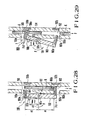
- Fig. 22 shows an application example of a unit structure wherein a swinging displacement of the bimorph element I is extracted through a seesaw mechanism.
- Reference numeral 51 denotes a transmission lever connected to the operating end (free end) of the bimorph element 1; and 52, a seesaw mechanism pivotally supported by a shaft 53. Excess external force is absorbed by.the seesaw mechanism 52, thus further improving reliability of the bimorph actuator.
- the support 42 for supporting the bimorph element 1 is fixed on a base 40A.
- An upper case 40B covers the bimorph element 1 so as not to obstruct operation of the bimorph element 1.
- a U-shaped recess is formed at one end of the seesaw mechanism 52 and is loosely fitted with the transmission lever 51. The other end of the seesaw mechanism 52 externally extends through a notch 55 of the upper case 40B. The distal end of the extended portion swings in the directions indicated by arrows upon vibration of the bimorph element 1.
- a guide hole 57 and threaded bimorph electrode terminals 58 are formed in the base 40A so as to easily mount the base 40A to another fixed member.
- Displacement restraint mechanisms are mounted on end portions 59a and 59b of the seesaw mechanism 52 to restrain rotation of the seesaw mechanism'52 exceeding a predetermined angle.
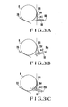
- Fig. 23 shows the main part of the mechanism used in Fig. 22.
- the magnet 60a is mounted on the seesaw mechanism 52 in the vicinity of the portion 52 which is engaged with the lever 51, as indicated by the dotted line.
- the magnetic member 60b is mounted at a position on the base 40A which corresponds to the magnet . 60a.
- a magnet 61a is mounted at an appropriate position of the seesaw mechanism so as to oppose the magnet 60a.
- a magnetic member 61b is mounted at a position of the base 40A which corresponds to the magnet 61a.
- the combination of the magnet and the magnetic member can be reversed.
- the two magnets can be magnetized with opposing polarities or can be arranged such that opposing poles face each other.
- Fig. 24 shows a construction wherein the lever and the seesaw mechanism shown in Figs. 22 and 23 are formed integrally.
- the free end of the bimorph element 1 is held by one end of the seesaw mechanism 52 to constitute a holding portion 52B.
- the operating portion of the seesaw mechanism 52 of Fig. 22 may be located in the left side, and the arm which is located to the right of the shaft 53 may be omitted, as indicated by the dotted line.
- the motion of the operating portion corresponds to that of the bimorph element.
- a ratio of a distance between the shaft 53 and the bimorph movable end connecting portion to a distance between the shaft 53 and the operating portion is properly selected, a displacement of the bimorph at the operating portion can be increased/decreased.
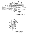
- a coin (rolling object) drop mechanism 120 comprises: a coin drop port formed midway on a guide plate constituting a coin guide 102; a lever member 122 as a drop port opening/closing mechanism supported pivotally about a shaft 122a perpendicular to the coin guide 102 so as to open/close a portion of the coin guide 102 which is located near the coin drop port 121; and the bimorph element 1 which has a lock portion 123a as a lock mechanism for locking the lever member 122 and which constitutes a coin drop drive mechanism.
- Reference numeral 124 denotes a base having a support 124a for supporting one.end portion of the bimorph element 1; and 125, a cover mounted on the base 124 to constitute a case and which holds the bimorph element 1 therein.
- the unit type bimorph element 1 has been described with reference to Figs. 19 to 24.
- Reference numerals 124b and 124c denote stoppers for regulating the swinging movement of the operating end of the bimorph element 1 within a predetermined range in the case.
- a engaging portion 122b is engaged with the lock portion 123a mounted on the proximal end of the lever member 122.
- a blocking piece 122c extends along one end of the lever member 122 to open/close the coin guide 102.
- the lever member 122 is arranged such that its blocking piece 122c is constantly biased by a torsion coil spring to block the coin guide 102.
- Reference numeral 127 denotes a stopper for stopping at a predetermined position the lever member 122 biased clockwise by a torsion spring.
- An opening 128 is formed in the other guide plate having a stopper surface 128a for receiving the blocking piece 122c when the blocking piece 122c is withdrawn from the coin guide 102.
- a photodetecting means 129 (129a and 129b) such as a photocoupler is arranged in the downstream side of the coin drop port 121 of the coin guide 102 to detect that the coin passes thereby.
- a biasing force is constantly applied by the drive input circuit 2 in Fig. 1 to displace the bimorph element 1 in the direction indicated by arrow i as shown in Fig. 26A.
- the lock portion 123a locks the engaging portion 122b of the proximal end of the lever member 122 so as to prevent the lever member 122 from being pivoted (counterclockwise) to withdraw from the coin guide 102.
- the blocking piece 122c of the lever member 122 extends into the coin guide 102 to close the portion of the coin guide 102 which is located near the coin drop port 122. Therefore, a coin K rolling along the guide 102 abuts against the blocking piece 122c to change the rolling .direction.
- the coin K is dropped through the drop port 121, as indicated by reference symbol K0.
- the bimorph element 1 When the polarity of the voltage applied to the bimorph element 1 is inverted, the bimorph element 1 is displaced in a direction indicated by arrow i as shown in Fig. 26A, and the lock portion 123a is released, so that the lever member 122 is biased by a spring constituting a restoration mechanism or by a self weight.
- the blocking piece 122c extends into the guide 102.
- the voltage is applied to the bimorph element 1 which is then displaced in the direction indicated by arrow i.
- the blocking piece of the lever member 122 extends unlocked into the coin guide 102.
- the coin K moves the blocking piece 122c against the biasing force due to its self weight and passes through the coin drop port 122.
- the lever member 122 returns to its initial state by means of the above-mentioned restoration mechanism.
- the photodetecting means 129 As the coin sensor constituted by a photocoupler or the like arranged in the downstream side of the coin guide 102, a voltage having the opposing polarity is applied to the bimorph element 1 again. Therefore, the lever member 122 is biased in the direction indicated by arrow i and is locked by the lock portion 123a.
- the lever 122 when the lever 122 returns to its initial position by the restoration mechanism such as a return spring, no force generated by the bimorph element 1 is required.
- the bimorph element 1 can generate only a small force.
- the bimorph element 1 generally requires low drive power and can perform low-power coin processing in addition to the effect described above.
- no large force acts on the bimorph element 1 during coin processing. Fatigue of the bimorph element 1 is thus small, resulting in.high reliability.
- a large force can be generated by the bimorph element 1 when a voltage is applied thereto so as to displace the bimorph element 1 in an opposite direction. Therefore, the opening/closing operation of the blocking piece 122c of the lever member 122 can be quickly controlled.
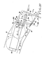
- Fig. 27 shows still another embodiment wherein the present invention is applied to another coin processing apparatus.
- a subsequent coin rolling stop arm mechanism and an opening/closing arm mechanism are formed integrally to-constitute an escape mechanism 160.
- the resultant assembly is driven by a bimorph element 1 so as to drop coins one by one toward the coin guide.
- An escape mechanism 160 has a substantially U-shaped escape 161 which is pivotally supported by a shaft 161a, as shown in Fig. 28.
- the escape 161 is pivoted by the bimorph element 1 through an engaging portion 161b as a driving force transmission mechanism.
- a blocking plate 163a of an opening/closing arm mechanism for opening/closing a coin drop port 162 is integrally formed with a lower end of the escape 161.
- a subsequent coin rolling stop pin 165 is integrally formed with the upper end of the escape 161 through an arm 164.
- Reference numeral 165a denotes a window for moving the pin 165 in the guide; and 166a and 166b, and 167a and 167b, permanent magnets mounted on the pin 165 and the blocking plate 163a, and on the opposing guide plate, respectively.
- the bimorph element 1 is normally displaced in the i direction to sequentially store the coins in the coin guide.
- the escape mechanism 160 receives a force for withdrawing the blocking piece by the weight of the coin K and a force for. preventing rotation of the blocking plate 163a due to-a frictional force between the coin and the blocking plate 163a.
- the rotational force becomes larger than the frictional force F C1 .
- the force F C1 shown in Fig. 30A acts on the opening/closing arm mechanism clockwise.
- the displacement and generating force characteristics of the bimorph element 1 are indicated by F B .
- the force F B becomes smaller than the force F C1 at the displacement near-end position of the bimorph element 1, so that the escape mechanism 160 is moved back until the forces are balanced. This is because the opening/closing mechanism 163 for minimizing the effective angular displacement of the escape mechanism 160 degrades stability when a coin is supported.
- a magnet mechanism consisting of 167a and 167b (magnets or a combination of a magnet and a magnetic member) are used to resolve the above problem.
- the attraction property of the magnet mechanism is represented by a force F M .
- the respective components are set to satisfy inequality F B1 + F M1 > F C1' so that the coin can be properly supported. When condition F M1 > F C1 is established, a voltage need not be applied to the bimorph element 1..
- the coin weight serves to withdraw the pin 165.
- the escape mechanism 160 may be pivoted in the direction indicated by the arrow against a frictional force between the coin and the pin 165 and a force of the bimorph element 1 along the i direction.
- Reference symbol F C2 denotes a force obtained by subtracting the frictional force from a pin withdrawal force; and FB1, a force of the bimorph element 1 along the j direction in the vicinity of the displacement near-end position.
- a line O-O connecting the gravity points of the leading coin and the subsequent coin becomes preferably parallel to the downstream portion of the coin guide 115 so as to prevent upward movement when the second coin abuts against the first coin.
- Ratios of a length a1 to a3, and a length a2 to a length a3 can be properly selected to amplify the displacement of the bimorph element 1.
- the escape mechanism 160 is directly controlled by the bimorph element. However, the escape mechanism 160 may be controlled through a arm mechanism, a link mechanism or a lock mechanism.
- each arm mechanism has a dynamically stable point in the vicinity of the displacement end position.
- Figs. 32 and 33 show still another embodiment of a coin processing apparatus according to the present invention.
- the present invention is applied to a coin discrimination mechanism or coin drop mechanism.
- reference numeral 251 denotes an opening/closing arm mechanism which has a blocking plate 251c at the distal end of an arm 251b.
- This arm 251 is pivotally supported by a shaft 251a mounted along the coin guide 102.
- a U-shaped groove mechanism 251d is arranged in the arm 251b to couple to the bimorph element.
- the opening/closing arm mechanism 251 is pivoted upon swinging of the bimorph element 1.
- the control circuit (reference numeral 5 in Fig. 1) is controlled to apply a voltage to the bimorph element 1 so as to hold the plate 251c in the opened/closed state.
- the bimorph element 1 is held displaced in a direction indicated by arrow i
- the blocking plate 251c at the lower end of the arm closes the drop port 250.
- the coin K passes on the plate 251c along the coin rail 115, as shown in Fig. 33.
- the opening/closing arm 251 is pivoted in the opening direction, so that the coin K is dropped downward by its self weight from the drop port 250.
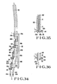
- Figs. 34 to 36 show still another embodiment of the present invention applied to a coin return mechanism.
- reference numeral 340 denotes a return door pivoted about a pivot shaft 340a.
- the door 340 is normally biased by a torsion coil spring 341 in a closed position in the same manner as the previous embodiment.
- An engaging piece 340b mounted at the upper end of the door 340 is selectively locked by a lock portion 323a constituting the lock mechanism at the distal end of the bimorph element 1.
- Coin dropping ports 342 formed at the terminals of coin storage guides 307A, 307B and 307C are closed by blocking pieces 309a, 309b and 309c, respectively.
- the bimorph element 1 is normally held displaced in the i direction to close the door 340.
- the bimorph element 1 is displaced in the opposite direction to open the door.
- the bimorph element is displaced to close the door 340.
- the bimorph element 1 is normally held displaced in the j direction, thereby causing the telephone set in a coin return enable state.
- a voltage is applied to the bimorph element which is then displaced in the i direction.
- the coin storage processing and the coin return operation at the end of conversation may be performed in accordance with the inversion of the voltage applied to the bimorph element 1.
- the above-mentioned telephone set is often deenergized when it is held in the on-hook state.
- a magnet mechanism may be used.
- a capacitor may be arranged to charge it with a predetermined voltage, so that the bimorph element 1 can be applied with a proper voltage as needed.
- the lock mechanism may be arranged toibe held in a mislocking. state.
- the bimorph element 1 is displaced in the direction to close the door 340.
- the bimorph element 1 is then displaced in the i direction to restore the initial state.
- the bimorph element 1 is normally displaced in the i direction,-and the door 340 is held in the open state.
- the polarity inversion is performed twice to reciprocate the bimorph element 1.
- This operation can also be applied to the case wherein the door 340 is set in the open state, i.e., the normal state, in the same manner as described above.
- Reference 343, 344 and 345 denote storage levers which are pivotally supported by shafts 343a, 344a and 345a and which are mounted at the terminals of the storage guides 307A, 307B and 307C, respectively.
- Coin drap guides 346A, 346B and 346C for guiding the coins to the safe are. located below the storage levers 343, 344 and 345.
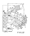
- Fig. 37 is an application example of a piezoelectric actuator using the bimorph element of the present invention.
- the piezoelectric actuators are used in a discrimination mechanism 390, coin drop mechanisms 308A, 308B and 308C, and a coin return mechanism 309.
- the construction of the actuators and a circuit arrangement thereof have been sufficiently described, and a detailed description thereof will be omitted.
- piezoelectric actuator units each having a bimorph element are used in the discrimination mechanism 390 and the coin return mechanism 309 to drive lock mechanisms 390a, respectively.
- Piezoelectric actuator units each having a bimorph element are used in members 391a, 392a and 393a to drive escape mechanisms 360A to 360C to constitute the coin drop mechanisms 308A to 308C, respectively.
- reference numeral 301 denotes a coin insertion port; and 302, a coin guide for guiding coins K (K10, K100 and K50) inserted from the coin insertion port 301.
- a coin detector 303 is arranged midway on the coin guide 302 to detect an insertion state of the coin and whether or not the inserted coin is authentic (K10, K100, K50) in accordance with an outer diameter, a material and a thickness thereof.
- a discrimination mechanism 304 is arranged next to the coin detector 303 to discriminate counterfeit or unfit coins in accordance with the detection signal from the coin detector 303 and returns the counterfeit and unfit coins to the return port.
- Coin selector mechanisms 305 and 306 select the authentic coins K (K10, K100 and K50) discriminated by the discrimination mechanism 304 and guided along the coin guide 302. This selection operation is performed in units of denominations of the authentic coins.
- the selected coins are guided to the coin drop guides 307A, 307B and 307C in units of denominations.
- the coin drop mechanisms 308A, 308B and 308C are formed at terminal portions of the coin drop guides 307A, 307B and 307C, respectively.
- the coin return mechanism 309 is arranged at the terminals of the coin drop guides 307A, 307B and 307C.
- the coin drop mechanisms 308A, 308B and 308C drop the coins in the safe, and the coin return mechanism 309 returns the coins to the return port.
- three types of coins K ( K 10, K100 and K50) are discriminated.
- Reference symbol K10 denotes a ⁇ 10 coin; K100, a ⁇ 100 coin; and K50, a ⁇ 50 coin.
- the opening/closing of the discrimination mechanism 304 is controlled by a controller 312 operated in response to the output signal. from the coin detector 303, and by a drive system (Fig. 1) consisting of the drive input circuit 2, the polarity switching circuit 3, the control circuit 5, the constant voltage circuit 4 and the power source E C .
- a drive system (Fig. 1) consisting of the drive input circuit 2, the polarity switching circuit 3, the control circuit 5, the constant voltage circuit 4 and the power source E C .
- Only the authentic coins K (K10, K100 and K50) among the inserted coins are guided along the coin guide 302 in the direction indicated by arrow a.
- counterfeit coins KO are.dropped from the coin guide 302 and are turned to the coin return port.
- authentic coins K (K10, K100 and K50) are selected in directions indicated by arrows c and d and arrows e and f by means of the coin selector mechanisms 305 and 306 under the control of the controller 312.
- the ⁇ 10 coin K10 is guided in a first coin drop guide 307A
- the ⁇ 100 coin K100 is guided in a second coin drop guide 307B
- the Y50 coin K50 is guided in a third coin drop guide 307C.
- the coins K (K10, K100 and K50) stored along the coin drop guides 307A, 307B and 307C drop by the coin drop mechanisms 308A, 308B and 308C one by one in the safe along the direction indicated by arrow g.
- the excessive coins are returned to the return port in the direction indicated by arrow h upon opening of the coin return mechanism 309 when the operation of main equipment having the coin processing apparatus is completed.
- sensors 329a and 329b are arranged at the output sides of the discrimination mechanism 390 and the coin drop mechanisms 308A to 308C to detect passage of the coins.
- the controller 312 detects operation of the sensors 329a and 329b, the polarity switching circuit 3 switches the polarity of the voltage through the control circuit 5.
- the present invention is not limited to the embodiments described above.
- the shape and construction of the respective components can be arbitrarily changed and modified.
- the piezo element need not be limited to the piezoceramic element, but can be extended to a ferroelectric material such as a polymeric resin having a piezoelectric effect.
- the present invention is applied to the coin processing apparatuses.
- the present invention may be used in a variety of applications so as to provide a drive unit for a known wire-dot printer head a micropump of an ink-jet printer, a relay, an optical switch or the like.
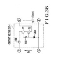
- the circuit shown in Fig. 1 generates a constant voltage.
- a constant voltage circuit 4 in Fig. 38 may be inserted in parallel with an input circuit of the polarity switching circuit 3.
- a constant current diode CRD, the emitter-collector path of a PNP transistor Trl, and the collector-emitter path of an NPN transistor Tr2 are connected in series with each other between a positive terminal F of the DC power source E C and the input side ⁇ of the polarity switching circuit 3.
- a resistor R100 is connected between the bases of the transistors Trl and-Tr2, and a Zener diode ZD4 is connected between the base of the transistor Tr2 and a terminal G.
- a charge current is supplied from the DC power source E C to the bimorph element 1 through the constant current diode CRD.
- the transistor Tr2 becomes OFF again. In this manner, the input terminal voltage is determined by V ZD4 . Even if the power source E C varies, a stable constant voltage can be obtained.
- the transistors Trl and Tr2 may be replaced with Darlington-connected PNP and NPN transistors. In this case, a more stable voltage can be obtained with low power.
Landscapes
- General Electrical Machinery Utilizing Piezoelectricity, Electrostriction Or Magnetostriction (AREA)
Applications Claiming Priority (16)
| Application Number | Priority Date | Filing Date | Title |
|---|---|---|---|
| JP232442/83 | 1983-12-09 | ||
| JP58232442A JPS60123993A (ja) | 1983-12-09 | 1983-12-09 | 貨幣返却装置 |
| JP59043881A JPS60190177A (ja) | 1984-03-09 | 1984-03-09 | 電歪振動装置 |
| JP43881/84 | 1984-03-09 | ||
| JP75623/84 | 1984-04-14 | ||
| JP59075623A JPS60219971A (ja) | 1984-04-14 | 1984-04-14 | 電歪振動装置駆動回路 |
| JP83700/84 | 1984-04-27 | ||
| JP59083700A JPS60229189A (ja) | 1984-04-27 | 1984-04-27 | 圧電駆動形硬貨処理装置 |
| JP59118257A JPS611278A (ja) | 1984-06-11 | 1984-06-11 | 圧電アクチユエ−タ |
| JP118257/84 | 1984-06-11 | ||
| JP152563/84 | 1984-07-23 | ||
| JP15256384A JPS6130974A (ja) | 1984-07-23 | 1984-07-23 | 圧電アクチユエ−タ |
| JP167328/84 | 1984-08-10 | ||
| JP59167328A JPS6145389A (ja) | 1984-08-10 | 1984-08-10 | 圧電駆動型転動物体処理装置 |
| JP59254243A JPS61135368A (ja) | 1984-12-03 | 1984-12-03 | 圧電アクチユエ−タ |
| JP254243/84 | 1984-12-03 |
Publications (3)
| Publication Number | Publication Date |
|---|---|
| EP0147112A2 true EP0147112A2 (de) | 1985-07-03 |
| EP0147112A3 EP0147112A3 (en) | 1988-11-23 |
| EP0147112B1 EP0147112B1 (de) | 1992-07-29 |
Family
ID=27572309
Family Applications (1)
| Application Number | Title | Priority Date | Filing Date |
|---|---|---|---|
| EP84308513A Expired - Lifetime EP0147112B1 (de) | 1983-12-09 | 1984-12-06 | Piezoelektrische Antriebsvorrichtung mit einem bilaminaren Element |
Country Status (5)
| Country | Link |
|---|---|
| US (1) | US4625137A (de) |
| EP (1) | EP0147112B1 (de) |
| KR (1) | KR890003388B1 (de) |
| CA (1) | CA1225694A (de) |
| DE (1) | DE3485851T2 (de) |
Cited By (8)
| Publication number | Priority date | Publication date | Assignee | Title |
|---|---|---|---|---|
| EP0388027A3 (de) * | 1989-03-14 | 1991-03-27 | Kabushiki Kaisha Toshiba | Eine Verschiebung erzeugende Anordnung |
| GB2271876A (en) * | 1992-10-22 | 1994-04-27 | Nat Rejectors Gmbh | Movable switch for coin handling machine |
| EP0678924A1 (de) * | 1994-04-22 | 1995-10-25 | ETAT FRANCAIS Représenté par le délÀ©gué général pour l'armement | Drückempfindliche Anordnung mit variabler Polarisation |
| FR2719160A1 (fr) * | 1994-04-22 | 1995-10-27 | France Etat Armement | Dispositif piézo-électrique à polarisation variable. |
| EP0767503A1 (de) * | 1995-10-05 | 1997-04-09 | Toyota Jidosha Kabushiki Kaisha | Verfahren und Einrichtung zur Steuerung eines piezoelektrischen Antriebs |
| FR2755275A1 (fr) * | 1996-10-24 | 1998-04-30 | Soc D Mecanique Et De Plastiqu | Dispositif d'encaissement ou de rejet de pieces de monnaie ou de jetons circulaires, et son procede de mise en oeuvre |
| US6335856B1 (en) | 1999-03-05 | 2002-01-01 | L'etat Francais, Represente Par Le Delegue Ministeriel Pour L'armement | Triboelectric device |
| WO2003090288A3 (en) * | 2002-04-15 | 2004-02-26 | Pbt Ip Ltd | Drive circuit for piezo ceramic device |
Families Citing this family (36)
| Publication number | Priority date | Publication date | Assignee | Title |
|---|---|---|---|---|
| US4708600A (en) * | 1986-02-24 | 1987-11-24 | Abujudom Ii David N | Piezoelectric fluid pumping apparatus |
| DE3751183T2 (de) * | 1986-09-29 | 1995-11-16 | Mitsubishi Chem Corp | Piezoelektrischer Antrieb. |
| WO1989007345A1 (en) * | 1988-02-08 | 1989-08-10 | Pacific Bell | Improved piezoelectric relay element and method for driving the same |
| US4916349A (en) * | 1988-05-10 | 1990-04-10 | Pacific Bell | Latching piezoelectric relay |
| EP0382465B1 (de) * | 1989-02-10 | 1993-06-16 | Seiko Epson Corporation | Treiberschaltung für einen Drahtpunktdruckknopf |
| US5071240A (en) * | 1989-09-14 | 1991-12-10 | Nikon Corporation | Reflecting optical imaging apparatus using spherical reflectors and producing an intermediate image |
| WO1994027330A1 (en) * | 1993-05-18 | 1994-11-24 | Telesensory Corporation | Method and apparatus for increasing bimorph displacement range |
| JPH08105806A (ja) * | 1994-10-03 | 1996-04-23 | Philips Japan Ltd | 圧電センサシステム |
| KR100393183B1 (ko) * | 1996-10-31 | 2003-10-17 | 삼성전자주식회사 | 마이크로액츄에이터의상보형정전구동장치 |
| US6139488A (en) * | 1997-09-25 | 2000-10-31 | Symphonix Devices, Inc. | Biasing device for implantable hearing devices |
| US6571643B1 (en) | 1998-08-13 | 2003-06-03 | Electronics For Imaging, Inc. | Ultrasound speed measurement of temperature and pressure effects |
| US6501625B1 (en) * | 1999-06-29 | 2002-12-31 | Hutchinson Technology Incorporated | Disk drive suspension with multi-layered piezoelectric actuator controlled gram load |
| JP3478227B2 (ja) * | 1999-08-03 | 2003-12-15 | 株式会社村田製作所 | 圧電体の分極方法 |
| JP2002156386A (ja) * | 2000-11-17 | 2002-05-31 | Fujitsu Ltd | 加速度センサ |
| JP3733861B2 (ja) * | 2001-02-01 | 2006-01-11 | 株式会社村田製作所 | 積層圧電体の分極方法 |
| TW546477B (en) * | 2001-08-09 | 2003-08-11 | Matsushita Electric Industrial Co Ltd | Drop impact determination system and acceleration sensing element used in the drop impact determination system |
| US7275412B2 (en) * | 2001-08-09 | 2007-10-02 | Matsushita Electric Industrial Co., Ltd. | Drop shock measurement system and acceleration sensor element used in the same |
| GB2390479A (en) * | 2002-06-06 | 2004-01-07 | Delphi Tech Inc | Poling method |
| US6979933B2 (en) * | 2002-09-05 | 2005-12-27 | Viking Technologies, L.C. | Apparatus and method for charging and discharging a capacitor |
| US7190102B2 (en) * | 2002-09-05 | 2007-03-13 | Viking Technologies, L.C. | Apparatus and method for charging and discharging a capacitor to a predetermined setpoint |
| US6908183B2 (en) * | 2002-10-31 | 2005-06-21 | Hewlett-Packard Development Company, L.P. | Fluid ejecting methods and related circuits |
| US7141911B2 (en) * | 2002-11-15 | 2006-11-28 | Matsushita Electric Industrial Co., Ltd. | Driving method of piezoelectric actuator, piezoelectric actuator, and disk recording and reproducing apparatus using the same |
| GB0304467D0 (en) * | 2003-02-26 | 2003-04-02 | 1 Ltd | Protective housing for ceramic actuators |
| ATE336804T1 (de) * | 2003-02-26 | 2006-09-15 | 1 Ltd | Schutzgehäuse für einen keramischen aktor |
| JP2005160028A (ja) * | 2003-10-27 | 2005-06-16 | Nec Tokin Corp | 撓み振動型エキサイタ |
| JP2006066655A (ja) * | 2004-08-27 | 2006-03-09 | Alps Electric Co Ltd | 電気機械エネルギー変換素子の駆動方法及び前記電気機械エネルギー変換素子の駆動装置 |
| JP2006116399A (ja) * | 2004-10-20 | 2006-05-11 | Citizen Electronics Co Ltd | 撓み振動型エキサイタ |
| KR101070944B1 (ko) * | 2006-07-11 | 2011-10-06 | 가부시키가이샤 무라타 세이사쿠쇼 | 압전 펌프 |
| CN101622451B (zh) * | 2007-12-03 | 2011-05-11 | 株式会社村田制作所 | 压电泵 |
| CN101350571B (zh) * | 2008-05-20 | 2010-12-01 | 浙江理工大学 | 压电陶瓷式电子提花机的压电陶瓷驱动电路 |
| US8847466B2 (en) * | 2008-06-19 | 2014-09-30 | Nxp B.V. | Piezoelectric bimorph switch |
| JP5743532B2 (ja) * | 2010-12-24 | 2015-07-01 | キヤノン株式会社 | 圧電デバイスの駆動方法 |
| WO2015077830A1 (en) * | 2013-11-29 | 2015-06-04 | Newcastle Innovation Limited | Systems and methods for driving piezoelectric benders |
| US10553381B2 (en) * | 2015-01-20 | 2020-02-04 | Electronics And Telecommunications Research Institute | Electrical switchgear for overcurrent protection using critical temperature device |
| KR102664394B1 (ko) | 2018-06-01 | 2024-05-08 | 삼성전자주식회사 | 이차원 물질을 포함하는 초격자 구조 및 이를 구비한 소자 |
| CN111551269B (zh) * | 2020-05-11 | 2021-09-10 | 浙江大学 | 一种基于形状记忆聚合物的结构健康监测系统 |
Family Cites Families (8)
| Publication number | Priority date | Publication date | Assignee | Title |
|---|---|---|---|---|
| US3110824A (en) * | 1960-10-31 | 1963-11-12 | Eastman Kodak Co | Piezoelectric actuating element |
| DE2109063C3 (de) * | 1971-02-25 | 1979-07-19 | Braun Ag | Piezoelektrischer Antrieb |
| US3794410A (en) * | 1973-02-20 | 1974-02-26 | Mca Disco Vision | Articulated mirror |
| US3821747A (en) * | 1973-04-23 | 1974-06-28 | Atomic Energy Commission | Recording system having piezoelectric stylus drive means |
| US4099211A (en) * | 1976-09-13 | 1978-07-04 | Ampex Corporation | Positionable transducing mounting structure and driving system therefor |
| GB2012106B (en) * | 1977-12-06 | 1982-06-23 | Sony Corp | Electro-mechanical transducers |
| JPS5492307A (en) * | 1977-12-29 | 1979-07-21 | Sony Corp | Driving circuit of electrostrictive converter |
| US4458171A (en) * | 1982-01-11 | 1984-07-03 | Piezo Electric Products, Inc. | Piezoelectric relay with tapered magnetic detent |
-
1984
- 1984-12-05 CA CA000469365A patent/CA1225694A/en not_active Expired
- 1984-12-05 US US06/678,482 patent/US4625137A/en not_active Expired - Fee Related
- 1984-12-06 DE DE8484308513T patent/DE3485851T2/de not_active Expired - Fee Related
- 1984-12-06 EP EP84308513A patent/EP0147112B1/de not_active Expired - Lifetime
- 1984-12-08 KR KR1019840007771A patent/KR890003388B1/ko not_active Expired
Cited By (16)
| Publication number | Priority date | Publication date | Assignee | Title |
|---|---|---|---|---|
| US5083056A (en) * | 1989-03-14 | 1992-01-21 | Kabushiki Kaisha Toshiba | Displacement generating apparatus |
| EP0388027A3 (de) * | 1989-03-14 | 1991-03-27 | Kabushiki Kaisha Toshiba | Eine Verschiebung erzeugende Anordnung |
| GB2271876A (en) * | 1992-10-22 | 1994-04-27 | Nat Rejectors Gmbh | Movable switch for coin handling machine |
| GB2271876B (en) * | 1992-10-22 | 1996-10-09 | Nat Rejectors Gmbh | A movable switch for a coin machine |
| EP0678924A1 (de) * | 1994-04-22 | 1995-10-25 | ETAT FRANCAIS Représenté par le délÀ©gué général pour l'armement | Drückempfindliche Anordnung mit variabler Polarisation |
| FR2719181A1 (fr) * | 1994-04-22 | 1995-10-27 | France Etat Armement | Dispositif piézo-sensible à polarisation variable. |
| FR2719160A1 (fr) * | 1994-04-22 | 1995-10-27 | France Etat Armement | Dispositif piézo-électrique à polarisation variable. |
| US5796206A (en) * | 1995-10-05 | 1998-08-18 | Kabushiki Kaisha Toyota Chuo Kenkyusho | Controller and controlling method for piezoelectric actuator |
| EP0767503A1 (de) * | 1995-10-05 | 1997-04-09 | Toyota Jidosha Kabushiki Kaisha | Verfahren und Einrichtung zur Steuerung eines piezoelektrischen Antriebs |
| FR2755275A1 (fr) * | 1996-10-24 | 1998-04-30 | Soc D Mecanique Et De Plastiqu | Dispositif d'encaissement ou de rejet de pieces de monnaie ou de jetons circulaires, et son procede de mise en oeuvre |
| EP0840261A1 (de) * | 1996-10-24 | 1998-05-06 | Asia Euro Industries Ltd. | Vorrichtung zur Einnahme oder Rückgabe von runden Münzen oder Wertmarken |
| US5901828A (en) * | 1996-10-24 | 1999-05-11 | Asia Euro Industries | Device for receiving or rejecting coins or circular tokens |
| AU736755B2 (en) * | 1996-10-24 | 2001-08-02 | Covadis Sa | Device for receiving or rejecting coins or circular tokens |
| AU736755C (en) * | 1996-10-24 | 2002-03-28 | Covadis Sa | Device for receiving or rejecting coins or circular tokens |
| US6335856B1 (en) | 1999-03-05 | 2002-01-01 | L'etat Francais, Represente Par Le Delegue Ministeriel Pour L'armement | Triboelectric device |
| WO2003090288A3 (en) * | 2002-04-15 | 2004-02-26 | Pbt Ip Ltd | Drive circuit for piezo ceramic device |
Also Published As
| Publication number | Publication date |
|---|---|
| DE3485851T2 (de) | 1993-03-18 |
| KR850005177A (ko) | 1985-08-21 |
| DE3485851D1 (de) | 1992-09-03 |
| EP0147112A3 (en) | 1988-11-23 |
| US4625137A (en) | 1986-11-25 |
| EP0147112B1 (de) | 1992-07-29 |
| KR890003388B1 (ko) | 1989-09-19 |
| CA1225694A (en) | 1987-08-18 |
Similar Documents
| Publication | Publication Date | Title |
|---|---|---|
| US4625137A (en) | Piezoelectric actuator using bimorph element | |
| US6411009B2 (en) | Piezoelectric actuator system | |
| EP0375250A2 (de) | Elektronischer Wecksignalgenerator | |
| EP0122370A1 (de) | Ansteuerschaltung für ein bistabiles Relais | |
| US5105142A (en) | Cell discharging circuit for a fuel cell | |
| KR970031145A (ko) | 재충전 가능한 전지장치(rechargeable battery apparatus) | |
| EP0083996B1 (de) | Elektronische Schaltvorrichtung mit Erregerwicklung | |
| CN1170294C (zh) | 具有由电磁铁保持电流供电的电源电路的电磁铁控制设备 | |
| JPH11234893A (ja) | 分離可能な電力接点を有する接点回路ブレーカ型装置用の制御装置 | |
| US4658155A (en) | Drive circuit for a piezoelectric actuator | |
| RU2187161C2 (ru) | Устройство управления электромагнитом | |
| CA1317345C (en) | Low power high voltage driver circuit | |
| JPS6257265A (ja) | 圧電素子駆動法 | |
| RU2074430C1 (ru) | Электромагнитный привод коммутационного аппарата | |
| EP0836263A1 (de) | Stromversorgung für elektronische uhr | |
| JPS6130975A (ja) | バイモルフ圧電振動装置ユニツト | |
| SU1497643A1 (ru) | Устройство дл управлени грузоподъемным электромагнитом | |
| JP2773788B2 (ja) | 電圧切換回路 | |
| JPS61135368A (ja) | 圧電アクチユエ−タ | |
| SU943905A1 (ru) | Устройство дл управлени электромагнитами | |
| SU1391952A1 (ru) | Устройство управлени печатающими молоточками | |
| SU1588615A1 (ru) | Устройство дл включени исполнительного реле железнодорожной автоматики | |
| JPS6130974A (ja) | 圧電アクチユエ−タ | |
| JPS6145389A (ja) | 圧電駆動型転動物体処理装置 | |
| US7057871B2 (en) | Actuation circuit for an electromagnetic actuator |
Legal Events
| Date | Code | Title | Description |
|---|---|---|---|
| PUAI | Public reference made under article 153(3) epc to a published international application that has entered the european phase |
Free format text: ORIGINAL CODE: 0009012 |
|
| 17P | Request for examination filed |
Effective date: 19841213 |
|
| AK | Designated contracting states |
Designated state(s): DE FR GB |
|
| RAP1 | Party data changed (applicant data changed or rights of an application transferred) |
Owner name: NIPPON TELEGRAPH AND TELEPHONE CORPORATION |
|
| PUAL | Search report despatched |
Free format text: ORIGINAL CODE: 0009013 |
|
| AK | Designated contracting states |
Kind code of ref document: A3 Designated state(s): DE FR GB |
|
| 17Q | First examination report despatched |
Effective date: 19901115 |
|
| GRAA | (expected) grant |
Free format text: ORIGINAL CODE: 0009210 |
|
| AK | Designated contracting states |
Kind code of ref document: B1 Designated state(s): DE FR GB |
|
| ET | Fr: translation filed | ||
| REF | Corresponds to: |
Ref document number: 3485851 Country of ref document: DE Date of ref document: 19920903 |
|
| PLBE | No opposition filed within time limit |
Free format text: ORIGINAL CODE: 0009261 |
|
| STAA | Information on the status of an ep patent application or granted ep patent |
Free format text: STATUS: NO OPPOSITION FILED WITHIN TIME LIMIT |
|
| 26N | No opposition filed | ||
| PGFP | Annual fee paid to national office [announced via postgrant information from national office to epo] |
Ref country code: FR Payment date: 19941010 Year of fee payment: 11 |
|
| PGFP | Annual fee paid to national office [announced via postgrant information from national office to epo] |
Ref country code: GB Payment date: 19941128 Year of fee payment: 11 |
|
| PGFP | Annual fee paid to national office [announced via postgrant information from national office to epo] |
Ref country code: DE Payment date: 19950228 Year of fee payment: 11 |
|
| PG25 | Lapsed in a contracting state [announced via postgrant information from national office to epo] |
Ref country code: GB Effective date: 19951206 |
|
| GBPC | Gb: european patent ceased through non-payment of renewal fee |
Effective date: 19951206 |
|
| PG25 | Lapsed in a contracting state [announced via postgrant information from national office to epo] |
Ref country code: FR Effective date: 19960830 |
|
| PG25 | Lapsed in a contracting state [announced via postgrant information from national office to epo] |
Ref country code: DE Effective date: 19960903 |
|
| REG | Reference to a national code |
Ref country code: FR Ref legal event code: ST |