EP0132520B1 - Verfahren zur Herstellung eines Halbleiterbauelementes - Google Patents
Verfahren zur Herstellung eines Halbleiterbauelementes Download PDFInfo
- Publication number
- EP0132520B1 EP0132520B1 EP84104927A EP84104927A EP0132520B1 EP 0132520 B1 EP0132520 B1 EP 0132520B1 EP 84104927 A EP84104927 A EP 84104927A EP 84104927 A EP84104927 A EP 84104927A EP 0132520 B1 EP0132520 B1 EP 0132520B1
- Authority
- EP
- European Patent Office
- Prior art keywords
- chip
- chips
- identification
- wafer
- module
- Prior art date
- Legal status (The legal status is an assumption and is not a legal conclusion. Google has not performed a legal analysis and makes no representation as to the accuracy of the status listed.)
- Expired - Lifetime
Links
Images
Classifications
-
- G—PHYSICS
- G06—COMPUTING; CALCULATING OR COUNTING
- G06K—GRAPHICAL DATA READING; PRESENTATION OF DATA; RECORD CARRIERS; HANDLING RECORD CARRIERS
- G06K7/00—Methods or arrangements for sensing record carriers, e.g. for reading patterns
- G06K7/10—Methods or arrangements for sensing record carriers, e.g. for reading patterns by electromagnetic radiation, e.g. optical sensing; by corpuscular radiation
- G06K7/10544—Methods or arrangements for sensing record carriers, e.g. for reading patterns by electromagnetic radiation, e.g. optical sensing; by corpuscular radiation by scanning of the records by radiation in the optical part of the electromagnetic spectrum
- G06K7/10821—Methods or arrangements for sensing record carriers, e.g. for reading patterns by electromagnetic radiation, e.g. optical sensing; by corpuscular radiation by scanning of the records by radiation in the optical part of the electromagnetic spectrum further details of bar or optical code scanning devices
- G06K7/10861—Methods or arrangements for sensing record carriers, e.g. for reading patterns by electromagnetic radiation, e.g. optical sensing; by corpuscular radiation by scanning of the records by radiation in the optical part of the electromagnetic spectrum further details of bar or optical code scanning devices sensing of data fields affixed to objects or articles, e.g. coded labels
-
- B—PERFORMING OPERATIONS; TRANSPORTING
- B07—SEPARATING SOLIDS FROM SOLIDS; SORTING
- B07C—POSTAL SORTING; SORTING INDIVIDUAL ARTICLES, OR BULK MATERIAL FIT TO BE SORTED PIECE-MEAL, e.g. BY PICKING
- B07C5/00—Sorting according to a characteristic or feature of the articles or material being sorted, e.g. by control effected by devices which detect or measure such characteristic or feature; Sorting by manually actuated devices, e.g. switches
- B07C5/34—Sorting according to other particular properties
- B07C5/3412—Sorting according to other particular properties according to a code applied to the object which indicates a property of the object, e.g. quality class, contents or incorrect indication
-
- H—ELECTRICITY
- H01—ELECTRIC ELEMENTS
- H01L—SEMICONDUCTOR DEVICES NOT COVERED BY CLASS H10
- H01L23/00—Details of semiconductor or other solid state devices
- H01L23/544—Marks applied to semiconductor devices or parts, e.g. registration marks, alignment structures, wafer maps
-
- H—ELECTRICITY
- H01—ELECTRIC ELEMENTS
- H01L—SEMICONDUCTOR DEVICES NOT COVERED BY CLASS H10
- H01L2223/00—Details relating to semiconductor or other solid state devices covered by the group H01L23/00
- H01L2223/544—Marks applied to semiconductor devices or parts
- H01L2223/54473—Marks applied to semiconductor devices or parts for use after dicing
-
- H—ELECTRICITY
- H01—ELECTRIC ELEMENTS
- H01L—SEMICONDUCTOR DEVICES NOT COVERED BY CLASS H10
- H01L2924/00—Indexing scheme for arrangements or methods for connecting or disconnecting semiconductor or solid-state bodies as covered by H01L24/00
- H01L2924/0001—Technical content checked by a classifier
- H01L2924/0002—Not covered by any one of groups H01L24/00, H01L24/00 and H01L2224/00
-
- Y—GENERAL TAGGING OF NEW TECHNOLOGICAL DEVELOPMENTS; GENERAL TAGGING OF CROSS-SECTIONAL TECHNOLOGIES SPANNING OVER SEVERAL SECTIONS OF THE IPC; TECHNICAL SUBJECTS COVERED BY FORMER USPC CROSS-REFERENCE ART COLLECTIONS [XRACs] AND DIGESTS
- Y10—TECHNICAL SUBJECTS COVERED BY FORMER USPC
- Y10S—TECHNICAL SUBJECTS COVERED BY FORMER USPC CROSS-REFERENCE ART COLLECTIONS [XRACs] AND DIGESTS
- Y10S438/00—Semiconductor device manufacturing: process
- Y10S438/94—Laser ablative material removal
Definitions
- This invention relates to a method of producing a semiconductor device. It involves the writing of unique identification data on each chip and the use of those data during subsequent fabrication steps.
- the fabrication of electrical components and in particular, integrated circuits typically employs fabrication techniques wherein slices or wafers of a semiconductive material, such as silicon, are processed to contain a large number of devices. That is, each wafer or slice contains a number of individual circuits.
- the wafers are configured to have areas facilitating dicing of the wafer into discrete integrated circuit chips.
- Batch processing techniques are conventionally used in the fabrication of such semiconductor wafers and dicing into integrated circuit chips. Following batch processing, the individual chips are then tested, sorted, and eventually placed on integrated circuit modules.
- U.S. Patent 4,150,331 discloses an individual chip identification utilizing programmable circuitry on the chip surface in which a signature for that chip may be encoded.
- diodes or other unidirectional current-conducting devices are connected between selected I/0 pins in a common bus which is connected to a test and diagnostic pin.
- a digital identification number is used by the placement of diodes such that the composite circuitry defines a chip signature in binary form.
- Such a technique while providing identification for an individual chip, is not human readable and requires specific I/O circuitry to determine the identification of a particular chip. Additionally, the technique uses valuable chip area that would otherwise be employed for fabrication of a device. Additionally, if comprehensive data is to be placed on the chip, an excessive number of logic devices are required. Additionally, electrical activity within the chip to interrogate the identification may be in error, resulting in a false identification.
- U.S. Patent 4,027,246 relates to an automated integrated circuit manufacturing system wherein each wafer physically carries an identification code.
- the system describes a technique for reading the identification for each of the wafers and then transporting the wafers in accordance with their identity from a random access wafer storage unit to subsequent processing steps.
- the system operates under computer control such that wafers are received from the random access storage station may be read and based on the identification of the wafer, selectively gated for fabrication into large scale integrated circuit devices.
- the system operates for purposes of identification at the wafer level and therefore once those components are diced, no affirmative identification of individual chips is made.
- Another object of this invention is to provide a system of semiconductor chip identification that is both human and machine readable.
- a further object of this invention is to provide a system of semiconductor chip identification that does not impinge on chip real estate and therefore does not impact circuit design.
- Yet a further object of this invention is to define a laser written chip identification system having an identification code that is usable at discrete production steps to eliminate manufacturing defects.
- the invention as claimed that, normally under computer control, provides for identification data on each chip which is readable by machine or by human under a low power magnifying glass.
- the identification information is placed on the back of each chip prior to dicing of the wafer.
- the system uses this identification throughout the areas of wafer test, dicing and selection, bonding/assembly/test fabrication and, during system test and field return units for defect analysis. That is, the identification is used throughout the life of the chip.
- the system in accordance with the present invention eliminates chip part number problems which occur on multi-chip substrate products.
- the laser written identification for a particular chip is read and verified against the chip part number required for that portion of the device. Any chip in the wrong place can therefore be corrected prior to soldering.
- the record of the chips forming that module can be obtained from chip identification records.
- chips while still on the wafer, are tested to generate data concerning chip performance, that is, categorizing the chips as being all good, defective, or partially usable. Those test results are then buffered in storage for further use.
- the chips are then individually scribed with a chip identification unique to that chip.
- the chip identification includes data concerning manufacturing codes delineating wafer type, part number, production controls, production line, date of manufacturing and the like. This is followed by the step of dicing the wafer.
- the chips are then sorted and placed in respective chip banks.
- the chips are read, that is, the identification is verified by having a reader determine whether the chip has been correctly placed in the proper cell of the chip bank for subsequent use.
- the bond/assemble/test level of manufacturing where, in accordance with computer control, chips are directed to proper placement at selected chip sites on a substrate.
- the identification of each chip is again ascertained to determine whether a defect problem exists, such as, the chip in the wrong site, the chip identification being unreadable due to rotation or other improper positioning of the chip or, actual chip damage. If an error in the chip identification comparison occurs, the problem is corrected and the chip re-read. When all the proper chips are properly placed on the substrate, reflow joining of the chips to the substrate occurs.
- the module is tested and field installed. If failures of the module occur at either stage, that is, system test returns or field returns, failure analysis occurs and given the positive chip identification of each stage in manufacture, comprehensive failure analysis can be made.
- this system encompasses four areas: wafer test (TEST), dicing and selection (DICE AND PICK), bond/assemble/test fabrication (BAT), and field returned units.
- the present invention virtually eliminates chip part number mix-up diffi culties which are common on multi-chip substrate devices.
- a wafer contains a number of areas which will ultimately be diced to form discrete chips. Tests are conducted vis-a-vis those chips while still on the wafer. Test data is generated relative to chip performance, that is, whether a chip is good/bad/or, only partially usable. The test results are then buffered for further use, that is, stored in the block "test data results".
- the second step shown (B) is to encode the individual chips.
- This step of chip identification utilizes a scribing tool to provide positive identification and test data relative to individual chips.
- data includes unique manufacturing codes which identify wafer type, part number and production controls, such as the production line, date of manufacture and the like. Additionally, data generated during testing at stage (A) is used to provide additional written data.
- the technique of scribing data for each chip on the wafer departs from that known in the prior art wherein only wafer serial numbers are generally provided.
- the wafer serial number is an identification generic to all chips but does not provide any unique identification for a particular chip on that wafer.
- the present invention extends the concept of identification to the chip level.
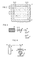
- Fig. 2 shows an example of a chip write area wherein a wafer 10 contains a chip 12.
- the hatched area is kerf to be sawed/diced away.
- the number of chips per wafer is variable upwards to several hundreds.
- the chip size can also vary.
- margin zones X and Y define areas about the circumference of the chip where scribing is forbidden. Additionally, if two lines are to be scribed, proper spacing between those lines must be delineated so that reading can take place.
- the number of characters of information C l -C i in the first line and C 1+1 -C in the second line are a function not only of chip size but also optical readability. Since human reading is desired, a minimum size is established to allow reading with a low power, unsophisticated optical system.
- scribing and reading on each chip is preferably done utilizing laser techniques.
- Such are known in the art, for example, used in conjunction with character-forming masks to scribe data on wafers.
- An example of a tool used for inscribing wafer serial numbers is shown in Figure 3 employing laser techniques as a writing instrument.
- Figure 3 illustrates a portion of the optics which would be used in conjunction with such a system to scribe chips.
- Figure 3 schematically illustrates a laser source 20 and a first optical system comprising beam expander lens 22 and 24. The beam 26 then passes through a diffuser 28 and is deflected onto the wafer 10 by a prism 30.
- a mask 32 may be a gold-plated molybdenum mask having a series of font forming a translucent reticle.
- the mask is rotated and the translucent font modulates the beam 26 where it is focused by projection lens 34 onto the wafer 10. Scribing then takes place by moving the mask in accordance with data scribing requirements.
- the identification data is formed by a diffraction pattern.
- the portion of the scribing beam that strikes the dislocated silicon is reflected in a diffused pattern.
- the bars scribed are a theta modulated pattern that reflects several orders of diffraction.
- Beam steering onto the scribing area shown in Figure 2 is accomplished by sweeping utilizing the prism 30 or any other known conventional beam steering technique.
- Such a device would utilize conventional storage techniques for identification and test data, such as floppy disc storage and reader verifying techniques to confirm that the wafer ID corresponds to the data input.
- step (C) the wafer is diced shown in step (C). Dicing is accomplished utilizing techniques known and established in the technology, such as diamond sawing.
- stage (D) includes a reading step to verify the selection and deposit process. Specifically, the back of each chip is read using data scribed in step (B). Errors, such as the wrong chip placed in the wrong bank, and/or the inability to read the chip ID caused by having the chip improperly placed, that is, rotated in the bank, are detected. Those defects together with others require that the chip be removed, corrected and/or replaced and then re-read in the bank. Chip holders called banks are common chip storage devices.
- a suitable reader is shown in Figure 4 utilizing techniques adapted from wafer readers.
- a laser source 40 typically a HeNe laser produces a beam 42 which is deflected by mirrors 44 and 46 onto a photodiode rosette 48.
- the photodiode 48 has a central opening through which the beam 42 passes through an encoder 52 onto the wafer 10.
- a reflected defraction pattern 50 occurs.
- the portion of the beam that strikes the dislocated silicon on the back of the chip is reflected in a diffused pattern. Since the characters formed by the laser reader are theta-modulated, the reflected defraction pattern for each character is perpendicular to its angular axis. Thus, the part that illuminates the edge of the theta-modulated bar will reflect several orders of defraction. By utilizing encoder techniques, the unique defraction pattern, that is, the pattern for each character which is perpendicular to its angular axis is detected. A rotating prism will cause the laser beam 42 to scan all digits of the chip identification.
- the bank is transported to the bond/assemble/test area (BAT) as shown in Figure 1, steps (F) through (J).
- BAT bond/assemble/test area
- steps (F) through (J) At this assembly site, a description of the module is furnished directing chip placement to a respective chip site on a substrate. That is, as shown, a particular chip i is directed to be placed at site j on a substrate.
- individual chips are placed on the module or substrate. The chips are not bonded.
- step (G) utilizing techniques shown in Figure 4 to verify their placement.
- the identification, unique to each chip is read and compared to the identification of the chip specified to be at that particular location in accordance with the module description.
- defects such as chip placed at the wrong site, or chips being rotated or mispositioned, or damaged, thereby rendering the identification unreadable, are detected. If an error in this comparison step occurs, the chips are corrected and the substrate re-read. Once it has been determined that the module has been correctly assembled, joining, typically by reflow solder techniques occurs, step (H).
- the present invention therefore offers an important advantage over the prior art since prior to actually joining the chips on the substrate, a positive determination is made concerning the correctness of the chip and its orientation on the substrate.
- the completed module is tested (I). If defective, the module may be reconfigured and laser scribed to provide additional module coded results. This additional scribing is significant since when the chip is pulled for rework, there is a low probability of pulling the wrong chip and the added information can be subsequently used for failure analysis. Thus, as shown in Figure 1, as a result of module testing, if no errors occur, the completed module is shipped for actual field use, (K). If, however, a problem is determined, reworking at step (J) occurs with additional scribing to provide additional information for subsequent failure analysis.
- Modules may fail as a result of handling during shipment or in actual use, (L).
- Defective modules are returned for failure analysis shown at step (M).
- An important aspect of the present invention is the use of the laser scribe identification data at step (B) to provide an accurate correlation of the individual chip which has failed, vis-a-vis manufacturing data. Thus, if a pattern evolves showing chips from one manufacturing run being defective or the like, an accurate indication exists concerning the production area requiring review and correction.
- Such failure analysis can, as shown in Figure 1, also take place as an adjunct to reworking defective modules discovered during the module test (I).
- the present invention provides by scribing on the back of an individual chip its history from manufacture through any rework. This history provides significant data allowing for failure analysis, thereby promoting chip yields and reducing defect levels in shipped products.
- FIG. 2 Another advantage of this invention as shown in Figure 2 is that the identification characters may be read by operators utilizing low power magnification.
- an individual chip may be optically read by a human operator.
- the present invention offers important advantages over prior art techniques of merely scribing wafers.
Claims (10)
Applications Claiming Priority (2)
| Application Number | Priority Date | Filing Date | Title |
|---|---|---|---|
| US06/507,311 US4510673A (en) | 1983-06-23 | 1983-06-23 | Laser written chip identification method |
| US507311 | 1983-06-23 |
Publications (3)
| Publication Number | Publication Date |
|---|---|
| EP0132520A2 EP0132520A2 (de) | 1985-02-13 |
| EP0132520A3 EP0132520A3 (en) | 1988-05-25 |
| EP0132520B1 true EP0132520B1 (de) | 1990-10-24 |
Family
ID=24018120
Family Applications (1)
| Application Number | Title | Priority Date | Filing Date |
|---|---|---|---|
| EP84104927A Expired - Lifetime EP0132520B1 (de) | 1983-06-23 | 1984-05-03 | Verfahren zur Herstellung eines Halbleiterbauelementes |
Country Status (4)
| Country | Link |
|---|---|
| US (1) | US4510673A (de) |
| EP (1) | EP0132520B1 (de) |
| JP (1) | JPS6010641A (de) |
| DE (1) | DE3483444D1 (de) |
Cited By (6)
| Publication number | Priority date | Publication date | Assignee | Title |
|---|---|---|---|---|
| EP0195966A2 (de) * | 1985-03-25 | 1986-10-01 | H&K Verpackungstechnik GmbH | Einrichtung zum Erkennen von Kennzeichenelementen an Transportanlagen für Stückgüter und dgl. |
| FR2652914A1 (fr) * | 1989-10-05 | 1991-04-12 | Pailler Andre | Systeme d'eclairage et de vision permettant la lecture automatique de caracteres graves a la surface de substrats semi-conducteurs. |
| EP0488053A1 (de) * | 1990-11-29 | 1992-06-03 | Tokyo Seimitsu Co.,Ltd. | Methode zur Herstellung eines Halbleiterchips |
| EP0578410A2 (de) * | 1992-07-09 | 1994-01-12 | Advanced Micro Devices, Inc. | Programmierbare Würfelidentifikationsschaltungen |
| US5570293A (en) * | 1990-11-29 | 1996-10-29 | Tokyo Seimitsu Co., Ltd. | Method and device for manufacturing a semiconductor chip |
| SG90756A1 (en) * | 1999-10-20 | 2002-08-20 | Tdk Corp | Method of reading mark and apparatus for the same |
Families Citing this family (76)
| Publication number | Priority date | Publication date | Assignee | Title |
|---|---|---|---|---|
| KR920007535B1 (ko) * | 1990-05-23 | 1992-09-05 | 삼성전자 주식회사 | 식별회로를 구비한 반도체 집적회로 칩 |
| US5410125A (en) * | 1990-10-11 | 1995-04-25 | Harry Winston, S.A. | Methods for producing indicia on diamonds |
| JP2845713B2 (ja) * | 1993-03-12 | 1999-01-13 | 株式会社東芝 | 並列ビットテストモード内蔵半導体メモリ |
| US5360747A (en) * | 1993-06-10 | 1994-11-01 | Xilinx, Inc. | Method of reducing dice testing with on-chip identification |
| TW276353B (de) * | 1993-07-15 | 1996-05-21 | Hitachi Seisakusyo Kk | |
| US8505108B2 (en) * | 1993-11-18 | 2013-08-06 | Digimarc Corporation | Authentication using a digital watermark |
| US6882738B2 (en) * | 1994-03-17 | 2005-04-19 | Digimarc Corporation | Methods and tangible objects employing textured machine readable data |
| US6644184B1 (en) * | 1995-02-09 | 2003-11-11 | Man Roland Druckmaschinen Ag | Offset printing machine |
| EP0712012A1 (de) * | 1994-11-09 | 1996-05-15 | International Business Machines Corporation | Authentizitätslabel und Authentizitätsmuster mit Beugungsstruktur und Methode zu deren Herstellung |
| FR2728104A1 (fr) * | 1994-12-09 | 1996-06-14 | Sgs Thomson Microelectronics | Procede de marquage de circuits integres avec un laser, et appareil de marquage s'y rapportant |
| KR970007379A (ko) * | 1995-07-19 | 1997-02-21 | 김주용 | 패턴층이 형성된 웨이퍼의 결함 다이 검사 방법 |
| US5932119A (en) * | 1996-01-05 | 1999-08-03 | Lazare Kaplan International, Inc. | Laser marking system |
| US5937270A (en) | 1996-01-24 | 1999-08-10 | Micron Electronics, Inc. | Method of efficiently laser marking singulated semiconductor devices |
| US5867505A (en) | 1996-08-07 | 1999-02-02 | Micron Technology, Inc. | Method and apparatus for testing an integrated circuit including the step/means for storing an associated test identifier in association with integrated circuit identifier for each test to be performed on the integrated circuit |
| US5927512A (en) | 1997-01-17 | 1999-07-27 | Micron Technology, Inc. | Method for sorting integrated circuit devices |
| US6100486A (en) | 1998-08-13 | 2000-08-08 | Micron Technology, Inc. | Method for sorting integrated circuit devices |
| US5844803A (en) * | 1997-02-17 | 1998-12-01 | Micron Technology, Inc. | Method of sorting a group of integrated circuit devices for those devices requiring special testing |
| US5915231A (en) * | 1997-02-26 | 1999-06-22 | Micron Technology, Inc. | Method in an integrated circuit (IC) manufacturing process for identifying and redirecting IC's mis-processed during their manufacture |
| US5856923A (en) * | 1997-03-24 | 1999-01-05 | Micron Technology, Inc. | Method for continuous, non lot-based integrated circuit manufacturing |
| US5907492A (en) * | 1997-06-06 | 1999-05-25 | Micron Technology, Inc. | Method for using data regarding manufacturing procedures integrated circuits (IC's) have undergone, such as repairs, to select procedures the IC's will undergo, such as additional repairs |
| US7120513B1 (en) * | 1997-06-06 | 2006-10-10 | Micron Technology, Inc. | Method for using data regarding manufacturing procedures integrated circuits (ICS) have undergone, such as repairs, to select procedures the ICS will undergo, such as additional repairs |
| US5877064A (en) * | 1997-07-15 | 1999-03-02 | Taiwan Semiconductor Manufacturing Co.Ltd | Method for marking a wafer |
| US6018686A (en) * | 1997-10-31 | 2000-01-25 | Cypress Semiconductor Corp. | Electrically imprinting a semiconductor die with identifying information |
| US6154872A (en) | 1997-11-20 | 2000-11-28 | Cypress Semiconductor Corporation | Method, circuit and apparatus for preserving and/or correcting product engineering information |
| US6052319A (en) | 1997-12-04 | 2000-04-18 | Cypress Semiconductor Corp. | Apparatus and method for controlling experimental inventory |
| US6148279A (en) | 1997-12-04 | 2000-11-14 | Cypress Semiconductor Corporation | Apparatus for recording and/or reading program history |
| US6049624A (en) | 1998-02-20 | 2000-04-11 | Micron Technology, Inc. | Non-lot based method for assembling integrated circuit devices |
| US6268641B1 (en) | 1998-03-30 | 2001-07-31 | Kabushiki Kaisha Toshiba | Semiconductor wafer having identification indication and method of manufacturing the same |
| US6181615B1 (en) | 1998-03-30 | 2001-01-30 | Cypress Semiconductor Corporation | Circuitry, apparatus and method for embedding quantifiable test results within a circuit being tested |
| US6209110B1 (en) | 1998-03-30 | 2001-03-27 | Cypress Semiconductor Corporation | Circuitry, apparatus and method for embedding a test status outcome within a circuit being tested |
| US7313253B2 (en) * | 1998-09-11 | 2007-12-25 | Digimarc Corporation | Methods and tangible objects employing machine readable data in photo-reactive materials |
| US6417484B1 (en) | 1998-12-21 | 2002-07-09 | Micron Electronics, Inc. | Laser marking system for dice carried in trays and method of operation |
| US6262388B1 (en) | 1998-12-21 | 2001-07-17 | Micron Electronics, Inc. | Laser marking station with enclosure and method of operation |
| US6161213A (en) * | 1999-02-17 | 2000-12-12 | Icid, Llc | System for providing an integrated circuit with a unique identification |
| JP4951811B2 (ja) * | 1999-03-24 | 2012-06-13 | 富士通セミコンダクター株式会社 | 半導体装置の製造方法 |
| JP2000294607A (ja) * | 1999-04-08 | 2000-10-20 | Hitachi Ltd | 半導体装置の製造方法 |
| ATE516598T1 (de) * | 1999-09-28 | 2011-07-15 | Kaneka Corp | Verfahren zur steuerung des herstellungsprozesses einer photoelektrischen wandlervorrichtung |
| DE19951048C2 (de) * | 1999-10-22 | 2002-11-21 | Infineon Technologies Ag | Verfahren zur Identifizierung einer integrierten Schaltung |
| EP1249042A1 (de) | 2000-01-20 | 2002-10-16 | Zavitan Semiconductors, Inc. | Kundenspezifische hardware |
| US6528760B1 (en) | 2000-07-14 | 2003-03-04 | Micron Technology, Inc. | Apparatus and method using rotational indexing for laser marking IC packages carried in trays |
| US6524881B1 (en) * | 2000-08-25 | 2003-02-25 | Micron Technology, Inc. | Method and apparatus for marking a bare semiconductor die |
| US6415977B1 (en) * | 2000-08-30 | 2002-07-09 | Micron Technology, Inc. | Method and apparatus for marking and identifying a defective die site |
| US6492706B1 (en) | 2000-12-13 | 2002-12-10 | Cypress Semiconductor Corp. | Programmable pin flag |
| US7316934B2 (en) * | 2000-12-18 | 2008-01-08 | Zavitan Semiconductors, Inc. | Personalized hardware |
| KR100393214B1 (ko) * | 2001-02-07 | 2003-07-31 | 삼성전자주식회사 | 패드의 수를 최소화하기 위한 칩 식별 부호 인식 장치 및이를 내장한 반도체 장치 |
| JP4071476B2 (ja) * | 2001-03-21 | 2008-04-02 | 株式会社東芝 | 半導体ウェーハ及び半導体ウェーハの製造方法 |
| CN101330000B (zh) * | 2001-03-21 | 2011-06-08 | 株式会社东芝 | 具有id标记的半导体晶片,及从中生产半导体器件的方法和设备 |
| US6867856B1 (en) | 2001-07-19 | 2005-03-15 | Advanced Micro Devices, Inc. | Apparatus for reading marks on a semiconductor substrate |
| US6792365B2 (en) * | 2001-08-10 | 2004-09-14 | Micron Technology, Inc. | Sequential unique marking |
| US6555400B2 (en) | 2001-08-22 | 2003-04-29 | Micron Technology, Inc. | Method for substrate mapping |
| JP3870780B2 (ja) * | 2001-12-21 | 2007-01-24 | ヤマハ株式会社 | 半導体装置の製造方法 |
| US7169685B2 (en) * | 2002-02-25 | 2007-01-30 | Micron Technology, Inc. | Wafer back side coating to balance stress from passivation layer on front of wafer and be used as die attach adhesive |
| DE10216874A1 (de) * | 2002-04-17 | 2003-07-10 | Infineon Technologies Ag | Verfahren zum Ablegen einer Information auf einem Halbleiter-Chip eines Wafers sowie Halbleiter-Chip |
| DE10219346B4 (de) * | 2002-04-30 | 2010-10-07 | Osram Opto Semiconductors Gmbh | Verfahren zum Abbilden und Zuordnen von Eigenschaften von einer Mehrzahl auf einem Wafer angeordneter Funktionschips und Wafer mit einer Mehrzahl von Funktionschips und Referenzchips |
| DE10321403A1 (de) * | 2002-05-15 | 2003-12-04 | Infineon Technologies Ag | Verfahren zur Markierung von Schlechtteilen |
| DE10241141B4 (de) * | 2002-09-05 | 2015-07-16 | Infineon Technologies Ag | Halbleiter-Bauelement-Test-Verfahren für ein Halbleiter-Bauelement-Test-System mit reduzierter Anzahl an Test-Kanälen |
| DE10259049A1 (de) * | 2002-12-17 | 2004-07-15 | Infineon Technologies Ag | Integriertes Halbleitermodul |
| US7097107B1 (en) | 2003-04-09 | 2006-08-29 | Mobile-Mind, Inc. | Pseudo-random number sequence file for an integrated circuit card |
| US6954711B2 (en) * | 2003-05-19 | 2005-10-11 | Applied Materials, Inc. | Test substrate reclamation method and apparatus |
| US7275234B2 (en) * | 2003-09-09 | 2007-09-25 | International Business Machines Corporation | System and method of automatically generating kerf design data |
| DE102004027489B4 (de) * | 2004-06-04 | 2017-03-02 | Infineon Technologies Ag | Verfahren zum Anordnen von Chips eines ersten Substrats auf einem zweiten Substrat |
| US7479779B2 (en) * | 2004-06-08 | 2009-01-20 | Advantest Corporation | Image sensor test system |
| KR100674950B1 (ko) * | 2005-01-22 | 2007-01-26 | 삼성전자주식회사 | 기준 반도체 칩을 구비하는 반도체 기판 및 이를 이용한반도체 칩 어셈블리 방법 |
| JP2006267056A (ja) | 2005-03-25 | 2006-10-05 | Toshiba Corp | 半導体装置およびそのテスト方法 |
| US7657390B2 (en) * | 2005-11-02 | 2010-02-02 | Applied Materials, Inc. | Reclaiming substrates having defects and contaminants |
| DE102005061834B4 (de) * | 2005-12-23 | 2007-11-08 | Ioss Intelligente Optische Sensoren & Systeme Gmbh | Vorrichtung und Verfahren zum optischen Prüfen einer Oberfläche |
| DE102006001601B4 (de) * | 2006-01-11 | 2008-06-26 | Infineon Technologies Ag | Verfahren zur Herstellung eines Halbleiterwafers mit Rückseitenidentifizierung |
| US7684608B2 (en) * | 2006-02-23 | 2010-03-23 | Vistech Corporation | Tape and reel inspection system |
| US7544578B2 (en) * | 2007-01-03 | 2009-06-09 | International Business Machines Corporation | Structure and method for stochastic integrated circuit personalization |
| US8492072B2 (en) * | 2009-04-30 | 2013-07-23 | Infineon Technologies Ag | Method for marking objects |
| US9099481B2 (en) | 2013-03-15 | 2015-08-04 | Semiconductor Components Industries, Llc | Methods of laser marking semiconductor substrates |
| CN114972180A (zh) * | 2017-04-13 | 2022-08-30 | 英卓美特公司 | 用于预测在装配单元中的缺陷的方法 |
| US10964648B2 (en) | 2017-04-24 | 2021-03-30 | International Business Machines Corporation | Chip security fingerprint |
| US11063000B2 (en) * | 2019-01-29 | 2021-07-13 | Infineon Technologies Ag | Semiconductor package authentication feature |
| CN112718522B (zh) * | 2020-12-03 | 2022-07-12 | 常熟理工学院 | 镍钛丝计数检测及激光打标一体机 |
| CN113492114B (zh) * | 2021-09-08 | 2021-11-16 | 苏州贝克微电子有限公司 | 一种用于集成电路的半导体芯片测试方法及其测试装置 |
Citations (1)
| Publication number | Priority date | Publication date | Assignee | Title |
|---|---|---|---|---|
| US4419747A (en) * | 1981-09-14 | 1983-12-06 | Seeq Technology, Inc. | Method and device for providing process and test information in semiconductors |
Family Cites Families (7)
| Publication number | Priority date | Publication date | Assignee | Title |
|---|---|---|---|---|
| US3583561A (en) * | 1968-12-19 | 1971-06-08 | Transistor Automation Corp | Die sorting system |
| NL7313695A (nl) * | 1973-10-05 | 1975-04-08 | Philips Nv | Werkwijze voor het automatisch signaleren van halfge- rlichamen. |
| US4027246A (en) * | 1976-03-26 | 1977-05-31 | International Business Machines Corporation | Automated integrated circuit manufacturing system |
| GB1584343A (en) * | 1977-06-07 | 1981-02-11 | Tokyo Shibaura Electric Co | Apparatus for marking identification symbols on wafer |
| US4150331A (en) * | 1977-07-29 | 1979-04-17 | Burroughs Corporation | Signature encoding for integrated circuits |
| JPS568836A (en) * | 1979-07-03 | 1981-01-29 | Chiyou Lsi Gijutsu Kenkyu Kumiai | Manufacturing system for semiconductor device |
| GB2116748A (en) * | 1982-03-06 | 1983-09-28 | Plessey Co Plc | Automatic control of manufacture and testing |
-
1983
- 1983-06-23 US US06/507,311 patent/US4510673A/en not_active Expired - Lifetime
-
1984
- 1984-04-20 JP JP59078828A patent/JPS6010641A/ja active Granted
- 1984-05-03 DE DE8484104927T patent/DE3483444D1/de not_active Expired - Fee Related
- 1984-05-03 EP EP84104927A patent/EP0132520B1/de not_active Expired - Lifetime
Patent Citations (1)
| Publication number | Priority date | Publication date | Assignee | Title |
|---|---|---|---|---|
| US4419747A (en) * | 1981-09-14 | 1983-12-06 | Seeq Technology, Inc. | Method and device for providing process and test information in semiconductors |
Non-Patent Citations (1)
| Title |
|---|
| IBM Technical Disclosure Bulletin, Vol. 14, No. 4, Sept. 1971, page 1023, US; R.R. Jorgensen: "Decoding and encoding for product identification" * |
Cited By (9)
| Publication number | Priority date | Publication date | Assignee | Title |
|---|---|---|---|---|
| EP0195966A2 (de) * | 1985-03-25 | 1986-10-01 | H&K Verpackungstechnik GmbH | Einrichtung zum Erkennen von Kennzeichenelementen an Transportanlagen für Stückgüter und dgl. |
| EP0195966A3 (de) * | 1985-03-25 | 1989-01-11 | H&K Verpackungstechnik GmbH | Einrichtung zum Erkennen von Kennzeichenelementen an Transportanlagen für Stückgüter und dgl. |
| FR2652914A1 (fr) * | 1989-10-05 | 1991-04-12 | Pailler Andre | Systeme d'eclairage et de vision permettant la lecture automatique de caracteres graves a la surface de substrats semi-conducteurs. |
| EP0488053A1 (de) * | 1990-11-29 | 1992-06-03 | Tokyo Seimitsu Co.,Ltd. | Methode zur Herstellung eines Halbleiterchips |
| US5570293A (en) * | 1990-11-29 | 1996-10-29 | Tokyo Seimitsu Co., Ltd. | Method and device for manufacturing a semiconductor chip |
| EP0578410A2 (de) * | 1992-07-09 | 1994-01-12 | Advanced Micro Devices, Inc. | Programmierbare Würfelidentifikationsschaltungen |
| US5642307A (en) * | 1992-07-09 | 1997-06-24 | Advanced Micro Devices, Inc. | Die identifier and die indentification method |
| SG90756A1 (en) * | 1999-10-20 | 2002-08-20 | Tdk Corp | Method of reading mark and apparatus for the same |
| US6721443B1 (en) | 1999-10-20 | 2004-04-13 | Tdk Corporation | Method of reading mark and apparatus for the same |
Also Published As
| Publication number | Publication date |
|---|---|
| JPS6010641A (ja) | 1985-01-19 |
| US4510673A (en) | 1985-04-16 |
| EP0132520A3 (en) | 1988-05-25 |
| JPS6341209B2 (de) | 1988-08-16 |
| EP0132520A2 (de) | 1985-02-13 |
| DE3483444D1 (de) | 1990-11-29 |
Similar Documents
| Publication | Publication Date | Title |
|---|---|---|
| EP0132520B1 (de) | Verfahren zur Herstellung eines Halbleiterbauelementes | |
| US7137557B2 (en) | Semiconductor device and an information management system therefore | |
| KR100417751B1 (ko) | 집적 회로 디바이스들을 조립하기 위한 넌-로트식 방법 | |
| US7117063B2 (en) | Sorting a group of integrated circuit devices for those devices requiring special testing | |
| US4585931A (en) | Method for automatically identifying semiconductor wafers | |
| JP2006527922A (ja) | エッジをベースにした識別機能を有する半導体ウエハ | |
| JPH07335510A (ja) | 半導体装置およびその識別子付与方法およびその不良解析方法 | |
| JPH07235617A (ja) | 半導体装置 | |
| US20050280129A1 (en) | Semiconductor device and manufacturing method therefor | |
| JPS59136942A (ja) | 良品チツプ選別装置 | |
| JPH0973615A (ja) | 磁気ヘッドの検査データ収集方法 | |
| TW202325455A (zh) | 打標位置評估方法、裝置及可讀存儲介質 | |
| JPH1074240A (ja) | 文字位置検出方法 | |
| KR910007389B1 (ko) | 얼라이먼트 타켓(Alignment Target) 제조방법 | |
| Markley | Beam lead device and hybrid microcircuit testing | |
| JPH0473925A (ja) | 半導体ウエハのデータ管理方法 | |
| JPH0521586A (ja) | 半導体ウエーハカセツトおよびその識別装置 | |
| JPS6123334A (ja) | 半導体ウエハの試験装置 |
Legal Events
| Date | Code | Title | Description |
|---|---|---|---|
| PUAI | Public reference made under article 153(3) epc to a published international application that has entered the european phase |
Free format text: ORIGINAL CODE: 0009012 |
|
| 17P | Request for examination filed |
Effective date: 19841123 |
|
| AK | Designated contracting states |
Designated state(s): DE FR GB IT |
|
| PUAL | Search report despatched |
Free format text: ORIGINAL CODE: 0009013 |
|
| AK | Designated contracting states |
Kind code of ref document: A3 Designated state(s): DE FR GB IT |
|
| 17Q | First examination report despatched |
Effective date: 19891124 |
|
| GRAA | (expected) grant |
Free format text: ORIGINAL CODE: 0009210 |
|
| AK | Designated contracting states |
Kind code of ref document: B1 Designated state(s): DE FR GB IT |
|
| REF | Corresponds to: |
Ref document number: 3483444 Country of ref document: DE Date of ref document: 19901129 |
|
| ET | Fr: translation filed | ||
| ITF | It: translation for a ep patent filed |
Owner name: IBM - DR. ALFREDO BRAVI |
|
| ITTA | It: last paid annual fee | ||
| PLBE | No opposition filed within time limit |
Free format text: ORIGINAL CODE: 0009261 |
|
| STAA | Information on the status of an ep patent application or granted ep patent |
Free format text: STATUS: NO OPPOSITION FILED WITHIN TIME LIMIT |
|
| 26N | No opposition filed | ||
| PGFP | Annual fee paid to national office [announced via postgrant information from national office to epo] |
Ref country code: GB Payment date: 19950413 Year of fee payment: 12 |
|
| PG25 | Lapsed in a contracting state [announced via postgrant information from national office to epo] |
Ref country code: GB Effective date: 19960503 |
|
| PGFP | Annual fee paid to national office [announced via postgrant information from national office to epo] |
Ref country code: FR Payment date: 19960507 Year of fee payment: 13 |
|
| GBPC | Gb: european patent ceased through non-payment of renewal fee |
Effective date: 19960503 |
|
| PGFP | Annual fee paid to national office [announced via postgrant information from national office to epo] |
Ref country code: DE Payment date: 19970521 Year of fee payment: 14 |
|
| PG25 | Lapsed in a contracting state [announced via postgrant information from national office to epo] |
Ref country code: FR Free format text: LAPSE BECAUSE OF NON-PAYMENT OF DUE FEES Effective date: 19980130 |
|
| REG | Reference to a national code |
Ref country code: FR Ref legal event code: ST |
|
| PG25 | Lapsed in a contracting state [announced via postgrant information from national office to epo] |
Ref country code: DE Free format text: LAPSE BECAUSE OF NON-PAYMENT OF DUE FEES Effective date: 19990302 |