EP0090161A2 - Verfahren zum Herstellen von dynamischen Halbleiter-Speicherzellen mit wahlfreiem Zugriff (RAM) nach der Doppel-Polysilizium-Gate-Technologie - Google Patents
Verfahren zum Herstellen von dynamischen Halbleiter-Speicherzellen mit wahlfreiem Zugriff (RAM) nach der Doppel-Polysilizium-Gate-Technologie Download PDFInfo
- Publication number
- EP0090161A2 EP0090161A2 EP83101406A EP83101406A EP0090161A2 EP 0090161 A2 EP0090161 A2 EP 0090161A2 EP 83101406 A EP83101406 A EP 83101406A EP 83101406 A EP83101406 A EP 83101406A EP 0090161 A2 EP0090161 A2 EP 0090161A2
- Authority
- EP
- European Patent Office
- Prior art keywords
- oxide
- thick oxide
- region
- etching
- areas
- Prior art date
- Legal status (The legal status is an assumption and is not a legal conclusion. Google has not performed a legal analysis and makes no representation as to the accuracy of the status listed.)
- Granted
Links
- 238000000034 method Methods 0.000 title claims abstract description 48
- 229910021420 polycrystalline silicon Inorganic materials 0.000 title claims abstract description 18
- 229920005591 polysilicon Polymers 0.000 title claims abstract description 18
- ZOXJGFHDIHLPTG-UHFFFAOYSA-N Boron Chemical compound [B] ZOXJGFHDIHLPTG-UHFFFAOYSA-N 0.000 claims abstract description 28
- 229910052796 boron Inorganic materials 0.000 claims abstract description 27
- 230000008569 process Effects 0.000 claims abstract description 23
- 238000005468 ion implantation Methods 0.000 claims abstract description 22
- 238000003860 storage Methods 0.000 claims abstract description 22
- 229920002120 photoresistant polymer Polymers 0.000 claims abstract description 21
- 230000015654 memory Effects 0.000 claims abstract description 16
- 238000005530 etching Methods 0.000 claims abstract description 13
- 239000004065 semiconductor Substances 0.000 claims abstract description 11
- HAYXDMNJJFVXCI-UHFFFAOYSA-N arsenic(5+) Chemical compound [As+5] HAYXDMNJJFVXCI-UHFFFAOYSA-N 0.000 claims abstract description 7
- 238000004519 manufacturing process Methods 0.000 claims abstract description 7
- 238000009413 insulation Methods 0.000 claims description 18
- 238000002513 implantation Methods 0.000 claims description 15
- 229910052785 arsenic Inorganic materials 0.000 claims description 10
- RQNWIZPPADIBDY-UHFFFAOYSA-N arsenic atom Chemical compound [As] RQNWIZPPADIBDY-UHFFFAOYSA-N 0.000 claims description 10
- 238000002955 isolation Methods 0.000 claims description 9
- 238000007254 oxidation reaction Methods 0.000 claims description 9
- 230000003647 oxidation Effects 0.000 claims description 8
- KRHYYFGTRYWZRS-UHFFFAOYSA-N Fluorane Chemical compound F KRHYYFGTRYWZRS-UHFFFAOYSA-N 0.000 claims description 4
- 229910052581 Si3N4 Inorganic materials 0.000 claims description 4
- HQVNEWCFYHHQES-UHFFFAOYSA-N silicon nitride Chemical compound N12[Si]34N5[Si]62N3[Si]51N64 HQVNEWCFYHHQES-UHFFFAOYSA-N 0.000 claims description 4
- 229910052710 silicon Inorganic materials 0.000 claims description 3
- 239000010703 silicon Substances 0.000 claims description 3
- 230000007704 transition Effects 0.000 claims description 3
- 229910004298 SiO 2 Inorganic materials 0.000 claims description 2
- 238000001312 dry etching Methods 0.000 claims description 2
- 230000004048 modification Effects 0.000 claims description 2
- 238000012986 modification Methods 0.000 claims description 2
- 238000010301 surface-oxidation reaction Methods 0.000 claims description 2
- AHKZTVQIVOEVFO-UHFFFAOYSA-N oxide(2-) Chemical compound [O-2] AHKZTVQIVOEVFO-UHFFFAOYSA-N 0.000 claims 3
- GNFTZDOKVXKIBK-UHFFFAOYSA-N 3-(2-methoxyethoxy)benzohydrazide Chemical compound COCCOC1=CC=CC(C(=O)NN)=C1 GNFTZDOKVXKIBK-UHFFFAOYSA-N 0.000 claims 1
- FGUUSXIOTUKUDN-IBGZPJMESA-N C1(=CC=CC=C1)N1C2=C(NC([C@H](C1)NC=1OC(=NN=1)C1=CC=CC=C1)=O)C=CC=C2 Chemical compound C1(=CC=CC=C1)N1C2=C(NC([C@H](C1)NC=1OC(=NN=1)C1=CC=CC=C1)=O)C=CC=C2 FGUUSXIOTUKUDN-IBGZPJMESA-N 0.000 claims 1
- 239000007943 implant Substances 0.000 claims 1
- 230000000873 masking effect Effects 0.000 claims 1
- 239000000126 substance Substances 0.000 claims 1
- 238000012856 packing Methods 0.000 abstract description 2
- 241000293849 Cordylanthus Species 0.000 description 6
- 150000004767 nitrides Chemical class 0.000 description 3
- VYPSYNLAJGMNEJ-UHFFFAOYSA-N Silicium dioxide Chemical compound O=[Si]=O VYPSYNLAJGMNEJ-UHFFFAOYSA-N 0.000 description 2
- 230000008901 benefit Effects 0.000 description 2
- -1 boron ions Chemical class 0.000 description 2
- 230000000694 effects Effects 0.000 description 2
- 230000004888 barrier function Effects 0.000 description 1
- 210000003323 beak Anatomy 0.000 description 1
- 230000006399 behavior Effects 0.000 description 1
- 230000000903 blocking effect Effects 0.000 description 1
- 239000003990 capacitor Substances 0.000 description 1
- 230000008021 deposition Effects 0.000 description 1
- 238000013461 design Methods 0.000 description 1
- 238000009792 diffusion process Methods 0.000 description 1
- 238000010292 electrical insulation Methods 0.000 description 1
- 239000011810 insulating material Substances 0.000 description 1
- 230000035515 penetration Effects 0.000 description 1
- 238000000206 photolithography Methods 0.000 description 1
- 238000001020 plasma etching Methods 0.000 description 1
- 238000011160 research Methods 0.000 description 1
- 238000000926 separation method Methods 0.000 description 1
- 235000012239 silicon dioxide Nutrition 0.000 description 1
- 239000000377 silicon dioxide Substances 0.000 description 1
- 238000003631 wet chemical etching Methods 0.000 description 1
Images
Classifications
-
- H—ELECTRICITY
- H01—ELECTRIC ELEMENTS
- H01L—SEMICONDUCTOR DEVICES NOT COVERED BY CLASS H10
- H01L21/00—Processes or apparatus adapted for the manufacture or treatment of semiconductor or solid state devices or of parts thereof
- H01L21/02—Manufacture or treatment of semiconductor devices or of parts thereof
- H01L21/04—Manufacture or treatment of semiconductor devices or of parts thereof the devices having potential barriers, e.g. a PN junction, depletion layer or carrier concentration layer
- H01L21/18—Manufacture or treatment of semiconductor devices or of parts thereof the devices having potential barriers, e.g. a PN junction, depletion layer or carrier concentration layer the devices having semiconductor bodies comprising elements of Group IV of the Periodic Table or AIIIBV compounds with or without impurities, e.g. doping materials
- H01L21/26—Bombardment with radiation
- H01L21/263—Bombardment with radiation with high-energy radiation
- H01L21/265—Bombardment with radiation with high-energy radiation producing ion implantation
- H01L21/26506—Bombardment with radiation with high-energy radiation producing ion implantation in group IV semiconductors
- H01L21/26513—Bombardment with radiation with high-energy radiation producing ion implantation in group IV semiconductors of electrically active species
- H01L21/2652—Through-implantation
-
- H—ELECTRICITY
- H01—ELECTRIC ELEMENTS
- H01L—SEMICONDUCTOR DEVICES NOT COVERED BY CLASS H10
- H01L21/00—Processes or apparatus adapted for the manufacture or treatment of semiconductor or solid state devices or of parts thereof
- H01L21/02—Manufacture or treatment of semiconductor devices or of parts thereof
- H01L21/027—Making masks on semiconductor bodies for further photolithographic processing not provided for in group H01L21/18 or H01L21/34
- H01L21/033—Making masks on semiconductor bodies for further photolithographic processing not provided for in group H01L21/18 or H01L21/34 comprising inorganic layers
-
- H—ELECTRICITY
- H01—ELECTRIC ELEMENTS
- H01L—SEMICONDUCTOR DEVICES NOT COVERED BY CLASS H10
- H01L21/00—Processes or apparatus adapted for the manufacture or treatment of semiconductor or solid state devices or of parts thereof
- H01L21/02—Manufacture or treatment of semiconductor devices or of parts thereof
- H01L21/04—Manufacture or treatment of semiconductor devices or of parts thereof the devices having potential barriers, e.g. a PN junction, depletion layer or carrier concentration layer
- H01L21/18—Manufacture or treatment of semiconductor devices or of parts thereof the devices having potential barriers, e.g. a PN junction, depletion layer or carrier concentration layer the devices having semiconductor bodies comprising elements of Group IV of the Periodic Table or AIIIBV compounds with or without impurities, e.g. doping materials
- H01L21/26—Bombardment with radiation
- H01L21/263—Bombardment with radiation with high-energy radiation
- H01L21/265—Bombardment with radiation with high-energy radiation producing ion implantation
- H01L21/266—Bombardment with radiation with high-energy radiation producing ion implantation using masks
-
- H—ELECTRICITY
- H01—ELECTRIC ELEMENTS
- H01L—SEMICONDUCTOR DEVICES NOT COVERED BY CLASS H10
- H01L21/00—Processes or apparatus adapted for the manufacture or treatment of semiconductor or solid state devices or of parts thereof
- H01L21/02—Manufacture or treatment of semiconductor devices or of parts thereof
- H01L21/04—Manufacture or treatment of semiconductor devices or of parts thereof the devices having potential barriers, e.g. a PN junction, depletion layer or carrier concentration layer
- H01L21/18—Manufacture or treatment of semiconductor devices or of parts thereof the devices having potential barriers, e.g. a PN junction, depletion layer or carrier concentration layer the devices having semiconductor bodies comprising elements of Group IV of the Periodic Table or AIIIBV compounds with or without impurities, e.g. doping materials
- H01L21/30—Treatment of semiconductor bodies using processes or apparatus not provided for in groups H01L21/20 - H01L21/26
- H01L21/31—Treatment of semiconductor bodies using processes or apparatus not provided for in groups H01L21/20 - H01L21/26 to form insulating layers thereon, e.g. for masking or by using photolithographic techniques; After treatment of these layers; Selection of materials for these layers
- H01L21/3105—After-treatment
- H01L21/311—Etching the insulating layers by chemical or physical means
- H01L21/31105—Etching inorganic layers
- H01L21/31111—Etching inorganic layers by chemical means
- H01L21/31116—Etching inorganic layers by chemical means by dry-etching
-
- H—ELECTRICITY
- H01—ELECTRIC ELEMENTS
- H01L—SEMICONDUCTOR DEVICES NOT COVERED BY CLASS H10
- H01L21/00—Processes or apparatus adapted for the manufacture or treatment of semiconductor or solid state devices or of parts thereof
- H01L21/70—Manufacture or treatment of devices consisting of a plurality of solid state components formed in or on a common substrate or of parts thereof; Manufacture of integrated circuit devices or of parts thereof
- H01L21/71—Manufacture of specific parts of devices defined in group H01L21/70
- H01L21/76—Making of isolation regions between components
- H01L21/762—Dielectric regions, e.g. EPIC dielectric isolation, LOCOS; Trench refilling techniques, SOI technology, use of channel stoppers
- H01L21/76202—Dielectric regions, e.g. EPIC dielectric isolation, LOCOS; Trench refilling techniques, SOI technology, use of channel stoppers using a local oxidation of silicon, e.g. LOCOS, SWAMI, SILO
- H01L21/76213—Dielectric regions, e.g. EPIC dielectric isolation, LOCOS; Trench refilling techniques, SOI technology, use of channel stoppers using a local oxidation of silicon, e.g. LOCOS, SWAMI, SILO introducing electrical inactive or active impurities in the local oxidation region, e.g. to alter LOCOS oxide growth characteristics or for additional isolation purpose
- H01L21/76216—Dielectric regions, e.g. EPIC dielectric isolation, LOCOS; Trench refilling techniques, SOI technology, use of channel stoppers using a local oxidation of silicon, e.g. LOCOS, SWAMI, SILO introducing electrical inactive or active impurities in the local oxidation region, e.g. to alter LOCOS oxide growth characteristics or for additional isolation purpose introducing electrical active impurities in the local oxidation region for the sole purpose of creating channel stoppers
-
- H—ELECTRICITY
- H10—SEMICONDUCTOR DEVICES; ELECTRIC SOLID-STATE DEVICES NOT OTHERWISE PROVIDED FOR
- H10B—ELECTRONIC MEMORY DEVICES
- H10B12/00—Dynamic random access memory [DRAM] devices
- H10B12/01—Manufacture or treatment
Definitions
- RAM random access memory
- the double polysilicon gate (Si 2 gate) process is to be regarded as the standard process for the implementation of dynamic RAM memories. Such a process for the manufacture of 16,384 bit dynamic random access memory is described in the IEEE Journal of Solid-State Circuits, Vol. Sc. 11, October 1976, pages 570 to 573.
- the minimum possible isolation distance of the LOCOS insulation is therefore twice the length of the bird's beak above the minimum structural dimension. It follows from this that in the case of the 256 K RAM memory cell known from the ISSCC 1980 volume, an additional space requirement of about 25% of the cell area is required. The higher space requirement for the insulation area leads to an increase in the total chip area. Another fundamental difficulty in reducing the insulation spacing arises from the so-called short channel effect of the thick oxide transistor. The thick oxide transistor loses its blocking capability for insulation distances of less than 2.5 / ⁇ m.
- HiC high capacity RAM cell concept
- the object on which the invention is based is now to produce dynamic RAM memory cells with double polysilicon gate technology in the direction of reducing the space requirement, simplifying the technological process and improving the electrical insulation between adjacent cells and thus increasing the dielectric strength.
- This object is achieved according to the invention by a method of the type mentioned at the outset in that the thickness of the oxide in the barrier region at the transitions between the thick oxide region and the thin oxide region is reduced both axially and laterally by etching using the photoresist mask provided for the arsenic and boron ion implantation , the photoresist edge being placed in the middle of the thick oxide region between the memory cell and thick oxide transistor.
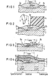
- FIGS. 1 to 4 illustrate the process flow according to an embodiment according to claim 2 in a sectional view.
- FIG. 1 shows a p-doped semiconductor body 1 (20 ohm.cm), on which the thick oxide layer 2 required for the separation of the active areas has been produced in a conventional manner using LOCOS technology.
- Boron doping has been introduced in a known manner under the thick oxide regions as a channel stop (setting the threshold voltage of about 1 volt), with boron ions having a dose of 2. 10 12 cm -2 and an energy of 120 keV before LOCOS oxidation using the nitride mask can be implanted on the active areas.
- the boron field implantation is designated by the reference number 3.
- the thick oxide layer 2 has a layer thickness of 650 nm, the thin oxide region 2a, 2b a layer thickness of 75 nm.
- the area of the minimum structural dimension List is shown above the sectional drawing.
- the storage areas are defined in which boron and arsenic ions 5a, 5b are implanted in the semiconductor body 1, the photoresist edge 4a being placed in the center of the insulation region (2, 2a, 2b).
- the oxide surface is then etched off, the thickness of the free thin oxide region 2a being reduced to 25 nm and the thickness of the free thick oxide region 2 being reduced to 600 nm.
- HiC implantation high capacity now takes place, with a lower-lying boron implantation 5a and then a flat arsenic implantation 5b being introduced into the storage area.
- the implantation parameters of the boron implantation 5a are selected so that both a maximum gain in the storage capacity and a sufficiently good dielectric strength of the storage diode is ensured, and the implantation is introduced sufficiently deep so that as much of the boron dose as possible covers the exposed thick oxide area 2 penetrates and increases the doping of the channel stop (3).
- the implantation dose is set to 7 ⁇ 10 12 Bcm -2 at an energy of 140 keV.
- the subsequent arsenic implantation 5b is used to set the threshold voltage in the storage area. Because of the low penetration depth (energy 100 keV, 1 x 10 14 Ascm -2 ), the arsenic cannot penetrate the thick oxide area 2.
- the implanted boron region is designated by reference number 6, the implanted arsenic region by 7.
- FIG. 3 In the next process step, the exposed thick and thin oxide areas (2, 2a) are overetched by 150 nm, whereby the bird's beak length (see arrow 8) is reduced to about 0.3 ⁇ m.
- the photoresist mask 4 is removed and a full overetch of the surface by 100 nm is connected.
- the bird's beak 8a of the storage area is reduced to approximately 0.25 ⁇ m at 350 nm field oxide thickness. For a typical 256 K cell design, this corresponds to a gain of 25 in the memory area.
- the bird's beak (8b) of the rest active areas is about 0.5 / ⁇ m.
- the insulation behavior of the thinned field oxide area (2) is significantly better than that of the undiluted areas (prior art) because of the increased boron doping.
- a gain in the reverse voltage of more than 10 V is achieved by the method according to the invention.
- FIG. 4 shows the arrangement after carrying out the gate oxidation (12), applying and structuring the polysilicon 1 electrode 9, producing the insulation oxide 10 and applying / structuring the polysilicon 2 electrode 11.
- FIG. 4 also shows the minimum structural dimensions L min and the length of the bird's beak L V.
- the active memory area of the cell, the area of a selection transistor and the isolation area are also marked in FIG. 4 by double or directional arrows.
- wet-chemical etching processes e.g. buffered hydrofluoric acid solutions
- reactive dry etching processes such as preferably the plasma etching process
- the entire overetching step can be carried out using the photoresist mask 4 (for the ion implantations) with 200 nm removal of the thick oxide transistor before the ion implantation (5a, 5b).
- the boron / arsenic ion implantation. is then introduced in the following step without scatter oxide, the energy of the boron ion implantation being reduced accordingly.
Landscapes
- Engineering & Computer Science (AREA)
- Physics & Mathematics (AREA)
- Manufacturing & Machinery (AREA)
- Microelectronics & Electronic Packaging (AREA)
- Power Engineering (AREA)
- General Physics & Mathematics (AREA)
- Condensed Matter Physics & Semiconductors (AREA)
- Computer Hardware Design (AREA)
- High Energy & Nuclear Physics (AREA)
- Chemical & Material Sciences (AREA)
- Inorganic Chemistry (AREA)
- Health & Medical Sciences (AREA)
- Toxicology (AREA)
- Chemical Kinetics & Catalysis (AREA)
- General Chemical & Material Sciences (AREA)
- Semiconductor Memories (AREA)
- Element Separation (AREA)
Abstract
Description
- Die vorliegende Patentanmeldung betrifft ein Verfahren zum Herstellen von dynamischen Halbleiter-Speicherzellen mit wahlfreiem Zugriff (RAM = random access memory) nach der Doppel-Polysilizium-Gate-Technologie mit einer ersten, auf dem Halbleiterkörper isoliert aufgebrachten Polysiliziumebene als Speicherelektrode für die im Halbleiterkörper erzeugten Speicherbereiche und einer, von der ersten Polysiliziumebene isoliert aufgebrachten zweiten Polysiliziumebene als Wortleitungen, bei dem die Isolation benachbarter aktiver Bereiche durch Dickoxidbereiche nach der bekannten LOCOS (= local oxidation of silicon)-Technologie erfolgt und bei dem zur Erhöhung der Zellkapazität in den Speicherbereich unter Verwendung einer Fotolackmaske eine flache Arsen- und eine tiefe Bor-Ionenimplantation durchgeführt wird.
- Der Doppel-Polysilizium-Gate (Si2-Gate)-Prozeßist als Standardprozeß für die Realisierung von dynamischen RAM-Speichern anzusehen. Ein solcher Prozeß für die Herstellung eines dynamischen 16.384-Bit-Speichers mit wahlfreiem Zugriff ist aus dem IEEE Journal of Solid-State Circuits, Vol. Sc. 11, Oktober 1976, Seite 570 bis 573 zu entnehmen.
- Mit der derzeit erreichbaren Strukturauflösung der Fotolithographie von etwa 1,5 /um wurde, wie aus dem Tagungsband ISSCC 15. Februar 1980 Digest of Techn. Papers, Seite 232/233 zu entnehmen ist, bereits eine 256-K-dynamische RAM-Speicherzelle realisiert. Die Isolation zwischen benachbarten aktiven Bereichen (Transistoren, Speicherkondensatoren, diffundierten Zonen) wird hierbei durch Dickoxidbereiche der sogenannten LOCOS-Technologie realisiert. Das LOCOS-Verfahren (= local oxidation of silicon) ist ein Isolationsverfahren für integrierte Schaltungen mit hoher Packungsdichte. Als Isoliermaterial zwischen den aktiven Bereichen wird Siliziumdioxid (Si02) verwendet. Nach selektiver Abscheidung einer Oxid- und einer Nitrid-Schicht erfolgt eine lokale Oxidation in der nitridfreien Zone, wobei eine starke laterale Unteroxidation (sogenannter Vogelschnabel, birds beak) und eine starke laterale Ausdiffusion der Feldimplantation, welche eine starke Weitenabhängigkeit der Einsatzspannung schmaler Transistoren zur Folge hat, stattfindet. LOCOS-Prozesse dieser Art sind aus den Philips-Research Reports, Vol. 26, Nr. 3, Juni 1971, auf den Seiten 157 bis 165 beschrieben. Bei dieser Isolationstechnik kann - wegen der graduellen Übergänge zwischen Dickoxid- und Dünnoxidbereichen (Vogelschnabel) von etwa 0,5 /um Länge - für den Isolationsabstand nicht die minimale Strukturabmessung realisiert werden. Der minimal mögliche Isolationsabstand der LOCOS-Isolation liegt deshalb um die doppelte Vogelschnabellänge über dem minimalen Strukturmaß. Daraus folgt, daß im Falle der aus dem Tagungsband ISSCC 1980 bekannten 256 K-RAM-Speicherzelle ein zusätzlicher Platzbedarf von etwa 25 % der Zellfläche erforderlich ist. Der höhere Platzbedarf für den Isolationsbereich führt zu einer Vergrößerung der Gesamtchipfläche. Eine weitere prinzipielle Schwierigkeit bei der Reduktion des Isolationsabstandes ergibt sich durch den sogenannten Kurzkanaleffekt des Dickoxidtransistors. Für Isolationsabstände kleiner 2,5 /um verliert der Dickoxidtransistor an Sperrfähigkeit.
- In einem Aufsatz von Tasch aus dem IEEE Journal of Electron Devices ED 25 (1973) Seite 33, wird ein HiC (high capacity)-RAM-Zellenkonzept vorgeschlagen, wobei in den Speicherbereich zur Erhöhung der Zellkapazität eine flache Arsen- und eine tiefe Bor-Ionenimplantation durchgeführt wird. Mit einer solchen Doppelimplantation wird die Zellkapazität einer 256 K-Speicherzelle um etwa 25 % erhöht.
- Die Aufgabe, die der Erfindung zugrundeliegt, besteht nun darin, dynamische RAM-Speicherzellen mit Doppel-Polysilizium-Gate-Technologie in Richtung Verkleinerung des Flächenbedarfs, Vereinfachung des technologischen Prozesses und Verbesserung der elektrischen Isolation zwischen benachbarten Zellen und damit einer Erhöhung der Spannungsfestigkeit herzustellen.
- Diese Aufgabe wird durch ein Verfahren der eingangs genannten Art erfindungsgemäß dadurch gelöst, daß die Dicke des Oxids im Sperrbereich an den Übergängen zwischen Dickoxidbereich und Dünnoxidbereich unter Verwendung der für die Arsen- und Bor-Ionenimplantation vorgesehenen Fotolackmaske durch Ätzen sowohl axial als auch lateral reduziert wird, wobei die Fotolack-Kante in die Mitte des Dickoxidbereichs zwischen Speicherzelle und Dickoxid-Transistor gelegt wird.
- .Es liegt im Rahmen der Erfindung die Verfahrensschritte wie folgt durchzuführen:
- a) Herstellen von Isolationsbereichen in Form von strukturierten SiO2-Schichten auf dem Halbleiterkörper zur Trennung der aktiven Bereiche nach dem sogenannten LOCOS- oder Isonlanarverfahren, wobei unmittelbar vor der LOCOS-Oxidation nach Maskierung der aktiven Bereiche mit einer Silizium-Nitridmaske eine ganzflächige Bor-Ionenimplantation zur Einstellung der Einsatzspannung der Isolationsbereiche durchgeführt wird,
- b) Entfernung der Silizium-Nitridmaske und Durchführung eines ganzflächigen Oxidationsprozesses,
- c) Aufbringen einer Fotolackmaske, wobei die Fotolack- Kante in die Mitte des Isolationsbereiches zwischen Speicherzelle und Dickoxid-Transistor gelegt wird,
- d) Abätzen des Oxids im Dickoxid- und Dünnoxidbereich auf eine Dicke des Dünnoxidbereichs im Speicherbereich von kleiner 30 nm,
- e) Erzeugung der Speicherbereiche durch eine Bor- und Arsen-Ionenimplantation, wobei die Bor-Ionenimplantation so geführt wird, daß sie den freiliegenden Dickoxidbereich durchdringt und die Bor-Dotierung unter dem Dickoxid erhöht und die Arsen-Ionenimplantation so durchgeführt wird, daß sie nur im aktiven Speicherbereich wirksam wird,
- f) Abätzen der nicht mit der Fotolackmaske abgedeckten Oxidschicht auf einen Wert, der etwa 2/3 der Ausgangsschichtdicke des Isolationsoxids entspricht,
- g) Entfernen der Fotolackmaske und ganzflächiges Abätzen der Oxidschichtoberfläche um weitere 100 nm,
- h) Erzeugen des Gateoxids, der ersten Polysilizium-Ebene, des Isolationsoxids und der zweiten Polysilizium- Ebene, sowie der Source/Drainbereiche, des Zwischenoxids und der Kontakte in bekannter Weise.
- Es ist aber auch möglich, in Abänderung dieser Verfahrensfolge, den gesamten Überätzschritt unter Verwendung der Fotolackmaske für die Speicher-Ionenimplantation vor der Implantation in einem einzigen Prozeß durchzuführen. Die Ionen-Implantation wird dann ohne Streuoxid durchgeführt, wobei die Energie der Bor-Ionenimplantation entsprechend zu reduzieren ist. Dies erfolgt durch Reduzierung der Implantationsenergie von 140 keV auf 100 keV.
- Besondere Ausgestaltungen ergeben sich aus den Unteransprüchen.
- Weitere Einzelheiten und Vorteile der Erfindung sind anhand der Figuren 1 bis 4, welche den Verfahrensablauf gemäß einem Ausführungsbeispiel nach Patentanspruch 2 im Schnittbild darstellen, noch näher erläutert.
- In allen Figuren gelten für gleiche Teile die gleichen Bezugszeichen.
- Figur 1 zeigt einen p-dotierten Halbleiterkörper 1 (20 Ohn·cm), auf den in herkömmlicher Weise nach der LOCOS-Technologie die für die Trennung der aktiven Bereiche erforderliche Dickoxidschicht 2 erzeugt worden ist. Unter den Dickoxidbereichen ist in bekannter Weise eine Bor-Dotierung als Kanalstop (Einstellung der Einsatzspannung von etwa 1 Volt) eingebracht worden, wobei Bor-Ionen mit einer Dosis von 2 . 1012 cm-2 und einer Energie von 120 keV vor der LOCOS-Oxidation unter Verwendung der Nitridmaske auf den aktiven Bereichen implantiert werden. Im folgenden ist die Bor-Feldimplantation mit dem Bezugszeichen 3 bezeichnet. Die Figur 1 zeigt den erfindungswesentlichen Teil der Anordnung nach dem Entfernen der Nitridmaske (der LOCOS-Prozeß ist, da bekannt, im einzelnen nicht dargestellt) und nach dem Aufoxidieren der Oberflächen. Die Dickoxidschicht 2 weist eine Schichtdicke von 650 nm, der Dünnoxidbereich 2a, 2b eine Schichtdicke von 75 nm auf. Der Bereich des minimalen Strukturmaßes List über dem Schnittbild eingezeichnet.
- In Figur 2 werden mit Hilfe einer Implantationsmaske 4 aus Fotolack die Speicherbereiche definiert, in dem Bor-und Arsen-Ionen 5a, 5b in den Halbleiterkörper 1 implantiert werden, wobei die Fotolackkante 4a in die Mitte des Isolationsbereiches (2, 2a, 2b) gelegt wird. Dann wird die Oxidoberfläche abgeätzt, wobei die Dicke des freien Dünnoxidbereiches 2a auf 25 nm und die Dicke des freien Dickoxidbereiches 2 auf 600 nm reduziert wird. Nun erfolgt die sogenannte HiC-Implantation (high capacity), wobei zunächst eine tiefer liegende Bor-Implantation 5a und dann eine flache Arsen-Implantation 5b in den Speicherbereich eingebracht wird. Die Implantationsparameter der Bor-Implantation 5a werden so gewählt, daß sowohl ein maximaler Gewinn in der Speicherkapazität und eine genügend gute Spannungsfestigkeit der Speicherdiode gewährleistet ist, als auch die Implantation genügend tief eingebracht wird, so daß möglichst ein großer Teil der Bordosis den freiliegenden Dickoxidbereich 2 durchdringt und die Dotierung des Kanalstops (3) erhöht. Im Ausführungsbeispiel wird die Implantationsdosis auf 7 x 10¹² Bcm-2 bei einer Energie von 140 keV eingestellt. Die nachfolgende Arsen-Implantation 5b dient der Einstellung der Einsatzspannung im Speicherbereich. Wegen der geringen Eindringtiefe (Energie 100 keV, 1 x 10¹⁴ Ascm-2) kann das Arsen den Dickoxidbereich 2 nicht durchdringen. Der implantierte Bor-Bereich ist mit dem Bezugszeichen 6,.der implantierte Arsen-Bereich mit 7 bezeichnet.
- Figur 3: Im nächsten Verfahrensschritt werden nun die freiliegenden Dick- und Dünnoxidbereiche (2, 2a) um 150 nm überätzt, wodurch die Vogelschnabellänge (siehe Pfeil 8) auf etwa 0,3 µm reduziert wird. Die Fotolackmaske 4 wird entfernt und eine ganzflächige Überätzung der Oberfläche um 100 nm angeschlossen. Dadurch wird der Vogelschnabel 8a des Speicherbereiches auf etwa 0,25 µm bei 350 nm Feldoxiddicke reduziert. Für ein typisches 256 K-Zelldesign entspricht dies einem Gewinn von 25 in der Speicherfläche. Der Vogelschnabel (8b)der übrigen aktiven Bereiche beträgt etwa 0,5 /um. Das Isolationsverhalten des gedünnten Feldoxidboreiches (2) ist wegen der erhöhten Bordotierung wesentlich besser als das der ungedünnten Bereiche (Stand der Technik). Durch das erfindungsgemäße Verfahren wird ein Gewinn in der Sperrspannung von mehr als 10 V erreicht.
- Wie aus Figur 4 zu entnehmen ist, ergibt sich als weiterer Vorteil des erfindungsgemäßen Verfahrens eine verbesserte Planarität der Bauelemente durch Versenken des Polysilizium-1-Dickoxidüberlapps. In der Figur 4 ist die Anordnung nach Durchführung der Gateoxidation (12), Aufbringen und Strukturierung der Polysilizium-1-Elektrode 9, Erzeugen des Isolationsoxids 10 und Aufbringen/Strukturieren der Polysilizium-2-Elektrode 11 dargestellt. Der Figur 4 sind ebenfalls die minimalen Strukturmaße Lmin sowie die Vogelschnabellänge LV zu entnehmen. In der Figur 4 ist auch der aktive Speicherbereich der Zelle, der Bereich eines Auswahltransistors und der Isolationsbereich durch Doppel- bzw. Richtungspfeile markiert.
- Als Ätzverfahren für das Dünnen der Isolationsschichten können naßchemische Ätzverfahren (z. B. gepufferte Flußsäurelösungen) und'auch reaktive Trockenätzverfahren, wie vorzugsweise das Plasmaätzverfahren verwendet werden.
- Alternativ zu der im Ausführungsbeispiel (Figur 1 bis 4) beschriebenen Verfahrensfolge kann der gesamte Überätzschritt unter Verwendung der Fotolackmaske 4 (für die Ionenimplantationen) bei 200 nm Abtrag des Dickoxidtransistors vor der Ionenimplantation (5a, 5b) durchgeführt werden. Die Bor-/Arsen-Ionenimplantation. wird dann in folgendem Schritt ohne Streuoxid eingebracht, wobei die Energie der Borionenimplantation entsprechend reduziert wird.
Claims (11)
Priority Applications (1)
| Application Number | Priority Date | Filing Date | Title |
|---|---|---|---|
| AT83101406T ATE23413T1 (de) | 1982-02-18 | 1983-02-14 | Verfahren zum herstellen von dynamischen halbleiter-speicherzellen mit wahlfreiem zugriff (ram) nach der doppel-polysilizium-gate- technologie. |
Applications Claiming Priority (2)
| Application Number | Priority Date | Filing Date | Title |
|---|---|---|---|
| DE3205858 | 1982-02-18 | ||
| DE19823205858 DE3205858A1 (de) | 1982-02-18 | 1982-02-18 | Verfahren zum herstellen von dynamischen halbleiter-speicherzellen mit wahlfreiem zugriff (ram) nach der doppel-polysilizium-gate-technologie |
Publications (3)
| Publication Number | Publication Date |
|---|---|
| EP0090161A2 true EP0090161A2 (de) | 1983-10-05 |
| EP0090161A3 EP0090161A3 (en) | 1984-05-16 |
| EP0090161B1 EP0090161B1 (de) | 1986-11-05 |
Family
ID=6156096
Family Applications (1)
| Application Number | Title | Priority Date | Filing Date |
|---|---|---|---|
| EP83101406A Expired EP0090161B1 (de) | 1982-02-18 | 1983-02-14 | Verfahren zum Herstellen von dynamischen Halbleiter-Speicherzellen mit wahlfreiem Zugriff (RAM) nach der Doppel-Polysilizium-Gate-Technologie |
Country Status (5)
| Country | Link |
|---|---|
| US (1) | US4414058A (de) |
| EP (1) | EP0090161B1 (de) |
| JP (1) | JPS58153363A (de) |
| AT (1) | ATE23413T1 (de) |
| DE (2) | DE3205858A1 (de) |
Cited By (1)
| Publication number | Priority date | Publication date | Assignee | Title |
|---|---|---|---|---|
| EP0209939A1 (de) * | 1985-07-11 | 1987-01-28 | Koninklijke Philips Electronics N.V. | Verfahren zum Herstellen einer Halbleiteranordnung |
Families Citing this family (11)
| Publication number | Priority date | Publication date | Assignee | Title |
|---|---|---|---|---|
| US4536947A (en) * | 1983-07-14 | 1985-08-27 | Intel Corporation | CMOS process for fabricating integrated circuits, particularly dynamic memory cells with storage capacitors |
| JPS60106142A (ja) * | 1983-11-15 | 1985-06-11 | Nec Corp | 半導体素子の製造方法 |
| US4570331A (en) * | 1984-01-26 | 1986-02-18 | Inmos Corporation | Thick oxide field-shield CMOS process |
| US4707457A (en) * | 1986-04-03 | 1987-11-17 | Advanced Micro Devices, Inc. | Method for making improved contact for integrated circuit structure |
| JP2886183B2 (ja) * | 1988-06-28 | 1999-04-26 | 三菱電機株式会社 | フィールド分離絶縁膜の製造方法 |
| US5234859A (en) * | 1988-06-28 | 1993-08-10 | Mitsubishi Denki Kabushiki Kaisha | LOCOS type field isolating film and semiconductor memory device formed therewith |
| WO1990005377A1 (en) * | 1988-10-31 | 1990-05-17 | Micron Technology, Inc. | Local encroachment reduction |
| US4959325A (en) * | 1989-02-24 | 1990-09-25 | Micron Technology, Inc. | Reduction of electric field effect in the bird's beak region of a DRAM cell following expansion of active region through local encroachment reduction |
| ATE217448T1 (de) * | 1990-01-22 | 2002-05-15 | Silicon Storage Tech Inc | Nichtflüchtige elektrisch veränderbare eintransistor-halbleiterspeicheranordnung mit rekristallisiertem schwebendem gate |
| US5332682A (en) * | 1990-08-31 | 1994-07-26 | Micron Semiconductor, Inc. | Local encroachment reduction |
| US6767794B2 (en) * | 1998-01-05 | 2004-07-27 | Advanced Micro Devices, Inc. | Method of making ultra thin oxide formation using selective etchback technique integrated with thin nitride layer for high performance MOSFET |
Citations (2)
| Publication number | Priority date | Publication date | Assignee | Title |
|---|---|---|---|---|
| US4112575A (en) * | 1976-12-20 | 1978-09-12 | Texas Instruments Incorporated | Fabrication methods for the high capacity ram cell |
| JPS5687359A (en) * | 1979-12-19 | 1981-07-15 | Fujitsu Ltd | Manufacture of one transistor type memory cell |
Family Cites Families (4)
| Publication number | Priority date | Publication date | Assignee | Title |
|---|---|---|---|---|
| US4075045A (en) * | 1976-02-09 | 1978-02-21 | International Business Machines Corporation | Method for fabricating FET one-device memory cells with two layers of polycrystalline silicon and fabrication of integrated circuits containing arrays of the memory cells charge storage capacitors utilizing five basic pattern deliberating steps |
| US4145803A (en) * | 1977-07-22 | 1979-03-27 | Texas Instruments Incorporated | Lithographic offset alignment techniques for RAM fabrication |
| DE2902665A1 (de) * | 1979-01-24 | 1980-08-07 | Siemens Ag | Verfahren zum herstellen von integrierten mos-schaltungen in silizium-gate- technologie |
| US4335502A (en) * | 1980-10-01 | 1982-06-22 | Standard Microsystems Corporation | Method for manufacturing metal-oxide silicon devices |
-
1982
- 1982-02-18 DE DE19823205858 patent/DE3205858A1/de not_active Withdrawn
- 1982-12-13 US US06/449,145 patent/US4414058A/en not_active Expired - Fee Related
-
1983
- 1983-02-14 EP EP83101406A patent/EP0090161B1/de not_active Expired
- 1983-02-14 AT AT83101406T patent/ATE23413T1/de not_active IP Right Cessation
- 1983-02-14 DE DE8383101406T patent/DE3367484D1/de not_active Expired
- 1983-02-17 JP JP58025462A patent/JPS58153363A/ja active Pending
Patent Citations (2)
| Publication number | Priority date | Publication date | Assignee | Title |
|---|---|---|---|---|
| US4112575A (en) * | 1976-12-20 | 1978-09-12 | Texas Instruments Incorporated | Fabrication methods for the high capacity ram cell |
| JPS5687359A (en) * | 1979-12-19 | 1981-07-15 | Fujitsu Ltd | Manufacture of one transistor type memory cell |
Non-Patent Citations (1)
| Title |
|---|
| PATENT ABSTRACTS OF JAPAN, Band 5, Nr. 159 (E-77)(831), 14 Oktober 1981 & JP - A - 56 87359 (FUJITSU K.K.) 15.07.1981 * |
Cited By (1)
| Publication number | Priority date | Publication date | Assignee | Title |
|---|---|---|---|---|
| EP0209939A1 (de) * | 1985-07-11 | 1987-01-28 | Koninklijke Philips Electronics N.V. | Verfahren zum Herstellen einer Halbleiteranordnung |
Also Published As
| Publication number | Publication date |
|---|---|
| US4414058A (en) | 1983-11-08 |
| ATE23413T1 (de) | 1986-11-15 |
| DE3205858A1 (de) | 1983-08-25 |
| JPS58153363A (ja) | 1983-09-12 |
| DE3367484D1 (en) | 1986-12-11 |
| EP0090161B1 (de) | 1986-11-05 |
| EP0090161A3 (en) | 1984-05-16 |
Similar Documents
| Publication | Publication Date | Title |
|---|---|---|
| DE3844388C2 (de) | ||
| EP0002670B1 (de) | Verfahren zum Herstellen eines bipolaren Transistors in einem Halbleitersubstrat | |
| DE3916228C2 (de) | Halbleiterspeichervorrichtung mit Stapelkondensatorzellenstruktur und Verfahren zu ihrer Herstellung | |
| EP0018501B1 (de) | Verfahren zur Herstellung von hochverdichteten vertikalen FETs und eine daraus gebildete Matrixanordnung | |
| DE69329376T2 (de) | Verfahren zur Herstellung einer SOI-Transistor-DRAM | |
| DE69221530T2 (de) | Verfahren zum Erhöhen der Kapazität eines DRAMs durch Anodisieren der Polysiliziumschicht einer unteren Kondensatorplatte | |
| DE4201004C2 (de) | Verfahren zur Bildung eines Kondensators | |
| DE3780369T2 (de) | Verfahren zum herstellen einer halbleiterstruktur. | |
| DE3880750T2 (de) | Vertikale Transistor-/Kapazitätspeicherzellen-Struktur und Herstellungsverfahren dafür. | |
| DE4136420C2 (de) | Verfahren zur Bildung eines Kondensators | |
| DE3012363C2 (de) | Verfahren zur Bildung der Kanalbereiche und der Wannen von Halbleiterbauelementen | |
| DE2756855A1 (de) | Verfahren zum herstellen einer matrix aus speicherzellen mit hoher speicherkapazitaet | |
| DE2809233A1 (de) | Halbleitervorrichtung und verfahren zu ihrer herstellung | |
| DE4301690A1 (de) | ||
| DE3029125A1 (de) | Halbleiterspeicher | |
| DE2928923C2 (de) | ||
| DE4229363A1 (de) | Verfahren zur bildung eines kondensators | |
| DE2741152A1 (de) | Speicherzelle fuer einen silizium- gate-n-kanal-mos-direktzugriffspeicher und verfahren zu ihrer herstellung | |
| DE3787687T2 (de) | Halbleiterspeicher. | |
| DE4028488A1 (de) | Halbleiterspeichervorrichtung und verfahren zu ihrer herstellung | |
| DE2933849A1 (de) | Verfahren zur herstellung von halbleiteranordnungen | |
| DE2716691A1 (de) | Feldeffekttransistor und verfahren zu dessen herstellung | |
| EP0090161B1 (de) | Verfahren zum Herstellen von dynamischen Halbleiter-Speicherzellen mit wahlfreiem Zugriff (RAM) nach der Doppel-Polysilizium-Gate-Technologie | |
| DE4007582C2 (de) | Verfahren zum Herstellen von mindestens zwei Kontakten in einem Halbleiterbauelement | |
| DE69132998T2 (de) | Speicheranordnung mit wahlfreiem Zugriff und Herstellungsverfahren dafür |
Legal Events
| Date | Code | Title | Description |
|---|---|---|---|
| PUAI | Public reference made under article 153(3) epc to a published international application that has entered the european phase |
Free format text: ORIGINAL CODE: 0009012 |
|
| AK | Designated contracting states |
Designated state(s): AT DE FR GB IT |
|
| PUAL | Search report despatched |
Free format text: ORIGINAL CODE: 0009013 |
|
| AK | Designated contracting states |
Designated state(s): AT DE FR GB IT |
|
| 17P | Request for examination filed |
Effective date: 19840528 |
|
| 17Q | First examination report despatched |
Effective date: 19860121 |
|
| GRAA | (expected) grant |
Free format text: ORIGINAL CODE: 0009210 |
|
| AK | Designated contracting states |
Kind code of ref document: B1 Designated state(s): AT DE FR GB IT |
|
| REF | Corresponds to: |
Ref document number: 23413 Country of ref document: AT Date of ref document: 19861115 Kind code of ref document: T |
|
| REF | Corresponds to: |
Ref document number: 3367484 Country of ref document: DE Date of ref document: 19861211 |
|
| ET | Fr: translation filed | ||
| PGFP | Annual fee paid to national office [announced via postgrant information from national office to epo] |
Ref country code: AT Payment date: 19870128 Year of fee payment: 5 |
|
| ITF | It: translation for a ep patent filed | ||
| PLBE | No opposition filed within time limit |
Free format text: ORIGINAL CODE: 0009261 |
|
| STAA | Information on the status of an ep patent application or granted ep patent |
Free format text: STATUS: NO OPPOSITION FILED WITHIN TIME LIMIT |
|
| 26N | No opposition filed | ||
| PG25 | Lapsed in a contracting state [announced via postgrant information from national office to epo] |
Ref country code: GB Effective date: 19890214 Ref country code: AT Effective date: 19890214 |
|
| GBPC | Gb: european patent ceased through non-payment of renewal fee | ||
| PG25 | Lapsed in a contracting state [announced via postgrant information from national office to epo] |
Ref country code: FR Free format text: LAPSE BECAUSE OF NON-PAYMENT OF DUE FEES Effective date: 19891027 |
|
| PG25 | Lapsed in a contracting state [announced via postgrant information from national office to epo] |
Ref country code: DE Effective date: 19891101 |
|
| REG | Reference to a national code |
Ref country code: FR Ref legal event code: ST |