EP0023510B1 - Memory organization for reducing peak current - Google Patents
Memory organization for reducing peak current Download PDFInfo
- Publication number
- EP0023510B1 EP0023510B1 EP80900356A EP80900356A EP0023510B1 EP 0023510 B1 EP0023510 B1 EP 0023510B1 EP 80900356 A EP80900356 A EP 80900356A EP 80900356 A EP80900356 A EP 80900356A EP 0023510 B1 EP0023510 B1 EP 0023510B1
- Authority
- EP
- European Patent Office
- Prior art keywords
- array
- sub
- row
- column
- sense
- Prior art date
- Legal status (The legal status is an assumption and is not a legal conclusion. Google has not performed a legal analysis and makes no representation as to the accuracy of the status listed.)
- Expired
Links
Images


Classifications
-
- G—PHYSICS
- G11—INFORMATION STORAGE
- G11C—STATIC STORES
- G11C11/00—Digital stores characterised by the use of particular electric or magnetic storage elements; Storage elements therefor
- G11C11/21—Digital stores characterised by the use of particular electric or magnetic storage elements; Storage elements therefor using electric elements
- G11C11/34—Digital stores characterised by the use of particular electric or magnetic storage elements; Storage elements therefor using electric elements using semiconductor devices
- G11C11/40—Digital stores characterised by the use of particular electric or magnetic storage elements; Storage elements therefor using electric elements using semiconductor devices using transistors
- G11C11/401—Digital stores characterised by the use of particular electric or magnetic storage elements; Storage elements therefor using electric elements using semiconductor devices using transistors forming cells needing refreshing or charge regeneration, i.e. dynamic cells
- G11C11/4063—Auxiliary circuits, e.g. for addressing, decoding, driving, writing, sensing or timing
- G11C11/407—Auxiliary circuits, e.g. for addressing, decoding, driving, writing, sensing or timing for memory cells of the field-effect type
- G11C11/409—Read-write [R-W] circuits
- G11C11/4091—Sense or sense/refresh amplifiers, or associated sense circuitry, e.g. for coupled bit-line precharging, equalising or isolating
-
- G—PHYSICS
- G11—INFORMATION STORAGE
- G11C—STATIC STORES
- G11C11/00—Digital stores characterised by the use of particular electric or magnetic storage elements; Storage elements therefor
- G11C11/21—Digital stores characterised by the use of particular electric or magnetic storage elements; Storage elements therefor using electric elements
- G11C11/34—Digital stores characterised by the use of particular electric or magnetic storage elements; Storage elements therefor using electric elements using semiconductor devices
- G11C11/40—Digital stores characterised by the use of particular electric or magnetic storage elements; Storage elements therefor using electric elements using semiconductor devices using transistors
- G11C11/401—Digital stores characterised by the use of particular electric or magnetic storage elements; Storage elements therefor using electric elements using semiconductor devices using transistors forming cells needing refreshing or charge regeneration, i.e. dynamic cells
- G11C11/403—Digital stores characterised by the use of particular electric or magnetic storage elements; Storage elements therefor using electric elements using semiconductor devices using transistors forming cells needing refreshing or charge regeneration, i.e. dynamic cells with charge regeneration common to a multiplicity of memory cells, i.e. external refresh
- G11C11/404—Digital stores characterised by the use of particular electric or magnetic storage elements; Storage elements therefor using electric elements using semiconductor devices using transistors forming cells needing refreshing or charge regeneration, i.e. dynamic cells with charge regeneration common to a multiplicity of memory cells, i.e. external refresh with one charge-transfer gate, e.g. MOS transistor, per cell
-
- G—PHYSICS
- G11—INFORMATION STORAGE
- G11C—STATIC STORES
- G11C11/00—Digital stores characterised by the use of particular electric or magnetic storage elements; Storage elements therefor
- G11C11/21—Digital stores characterised by the use of particular electric or magnetic storage elements; Storage elements therefor using electric elements
- G11C11/34—Digital stores characterised by the use of particular electric or magnetic storage elements; Storage elements therefor using electric elements using semiconductor devices
- G11C11/40—Digital stores characterised by the use of particular electric or magnetic storage elements; Storage elements therefor using electric elements using semiconductor devices using transistors
- G11C11/401—Digital stores characterised by the use of particular electric or magnetic storage elements; Storage elements therefor using electric elements using semiconductor devices using transistors forming cells needing refreshing or charge regeneration, i.e. dynamic cells
- G11C11/4063—Auxiliary circuits, e.g. for addressing, decoding, driving, writing, sensing or timing
Definitions
- This invention rleates to semiconductor memory devices, and finds application for example in a high density dynamic metal-oxide- semiconductor (MOS) random access memory (RAM) having an array of one transistor, one capacitor memory cells.
- MOS metal-oxide- semiconductor
- RAM random access memory
- MOS dynamic RAMs are known in the art. These memories are fabricated on a single silicon chip using known MOS technologies. Typically n-channel MOS technology is used because of its inherent performance advantages. In recent years there has been a rapid evolution of MOS dynamic RAMs toward increased density and higher performance. Each new generation of RAMs has provided a fourfold increase in storage capacity over those of the previous generation. This evolution has been made possible by advances in n-channel MOS technology and in wafer patterning techniques leading toward a shrinkage in the size of the memory cell. Today MOS RAMs having a storage capacity of 16,384 bits (i.e., 16K RAMs) are commercially available. Presently, manufacturers are starting to introduce a 65,536 bit, or 64K, RAM; see Electronics, September 28, 1978, pp. 109-116.
- the memory cell array is divided into two sub-arrays each having 128 rows and 256 columns.
- a two sub-array organization provides the advantage of having a refresh sequence (128 cycles) which is compatible with that of older generation RAMs by allowing simultaneous refresh of a row in each sub-array.
- a two sub-array organization also provides improved signals for sensing by virtue of having shorter bit-lines (column conductors) and, therefore, of reduced bit-line capacitance.
- the device includes an arrangement for reducing power dissipation when the RAM is in a read or a write mode, whereby only one of the two sub-arrays is fully selected for accessing a cell, i.e., both a row and a column are selected, while the other sub-array is partially selected for performing the refresh function only, i.e., only a row is selected. Therefore, the column decoders in the partially selected sub-array remains inactive to reduce both average and peak currents.
- the discharge of the capacitances coupled to the "low-going" sense amplifier nodes causes a transient surge of current primarily on the VSS power supply lines.
- the number of sense amplifiers required is increased (as many as 512 in a 64K RAM); and, therefore, the magnitude of the latching current peak also becomes greater.
- Large current peaks on various conductors in the memory chip interfere with proper memory operation by causing capacitive and inductive pickup of unwanted signals on other conductors and by causing voltage drops on the power supply nodes of various circuits in the memory.
- Electrodes May 13, 1976, describes at pages 81-86 a 16-k semiconductor memory device of the type comprising a multiplicity of memory cells arranged on a single chip in an ordered array of rows and columns.
- the array is divided into a plurality of sub-arrays, each sub-array having an associated row and column decoder means responsive to an address for selecting, respectively, a row and a column in the associated sub-array.
- Sense amplifiers are included for retrieving information from the memory cells.
- Patent Abstracts of Japan, Vol. 1, No. 155, December 12, 1977, page 8307 E77, relates to the use of a plurality of memory chips which may be connected together. Refresh current is delivered to the different chips in a staggered manner to reduce power line current surges external to each chip.
- a semiconductor memory device includes a multiplicity of memory cells arranged on a single chip in an ordered array of rows and columns, the array being divided into a plurality of sub-arrays, each sub-array having associated row and column decoder means responsive to an address for selecting, respectively, a row and a column in the associated sub-array, a plurality of sense/refresh amplifiers means, a different one associated with each column in each sub-array, for sensing and/or refreshing contents of a cell situated along a selected row, and is characterised in that corresponding rows of each of the plurality of sub-arrays are substantially simultaneously selected and the memory cells thereof refreshed during overlapping time periods, and there is included means responsive to a part of the address for fully selecting only one sub-array from which stored information may be retrieved, and means for activating after row selection the sense/refresh amplifier means in any given sub-array substantially simultaneously but activating the sense/refresh amplifier means of the different sub-arrays in sequence beginning with the fully selected sub
- a semiconductor memory device includes a multiplicity of memory cells arranged on a single chip in an ordered array of rows and columns, each row having a row conductor coupled to all cells in the row, each column having a column conductor coupled to all cells in the column, the array being divided into a plurality of sub-arrays each having associated row and column decoder means responsive to an address for selecting, respectively, a row and a column in the associated sub-array, a plurality of sense/refresh amplifier means, a different one coupled to each column conductor in each sub-array for sensing and/or refreshing the contents of each cell situated along a selected row, column precharge means coupled to each column conductor for maintaining each column conductor in a sub-array at a precharge potential before row selection therein, and is characterised by means responsive to a part of the address for fully selecting a single sub-array, and control means for releasing all the column conductors of all sub-arrays from the precharge potential prior to row selection and for recovering
- the invention of claim 1 provides a memory organization in which activation (latching) of the sense amplifiers in the sub-arrays is staggered. First the sense amplifiers in the fully selected sub-array in which a cell is to be accessed are substantially simultaneously latched. Then, after a delay sufficient to allow the current peaks caused by latching in the fully selected sub-array to subside, the sense amplifiers in the or a partially selected sub-array are substantially simultaneously latched. In addition, the recovery of column conductors to a precharge potential may also be staggered on a sub-array by sub-array basis. The or a partially selected sub-array in which only the refresh function takes place is recovered first.
- the fully selected sub-array is recovered after a delay sufficient to allow the current peak caused by the recovery of a partially selected sub-array to subside.
- the peak current of the improved memory is reduced as the current peaks from sense amplifier latching in each sub-array as well as those from column conductor recovery in each sub-array are made noncoincident.
- FIG. 1 there is shown a block diagram representative of a dynamic RAM embodying the invention.
- the RAM can be fabricated on a single silicon chip using n-channel MOS technology.
- the chip has 16 terminals or external connections; these include 8 multiplexed address input terminals AO to A7, external voltage terminals VDD, VSS, and VBB, a data output terminal Q, a data input terminal D, a row enable clock input terminal RE, a column enable clock input terminal CE and a write enable input terminal WE.
- the VDD, VSS, VBB, Q and D terminals are not shown in FIG. 1.
- the chip includes a memory cell array which is divided into two sub-arrays, an upper 1001, and a lower 1002.
- Each sub-array is bisected by a group of 256 sense amplifiers and 64 column decoders into two blocks each having 64 rows and 256 columns of cells to provide a total of 32,768 (32K) cells for each sub-array.
- the entire array has 65,536 (64K) cells.
- a row of 256 reference cells is also included in each block. The bisection of each sub-array being across the column conductors, two half-column conductors are created from each column conductor in the sub-array.
- An operating cycle for the memory begins when a row enable signal going from a TTL "high” logic level to a TTL “low” logic level is applied to the RE input to initiate the row clocks included in the timing generators 1009 which in turn strobe the 7 row address buffers 1010 and the CA8 column address buffer 1011.
- An 8-bit TTL level address previously applied to inputs AO to A7 is converted to MOS level row address signals RAO to RA6 and column address signal CAB.
- the MOS address signals are all double railed, that is, both the address bits and their complements are used for row selection. Therefore, each address signal includes both the address bit and its complement.
- the row address signals are used by the row decoders to select one row out of 128 in each sub-array.
- the row decoders which also select one of two reference rows in each sub-array are partitioned into four sections 1012 to 1015, one associated with each block. Each section consists of 16 individual row decoders each serving four rows. Selection of a row in one block of a sub-array also results in the selection of the corresponding or reference row in the other block of the sub-array.
- the CA8 address signal is used for various steering and enabling functions to determine which sub-array is to be fully selected. A fully selected sub-array is one in which both a row and a column are selected, whereas a partially selected sub-array is one in which only a row is selected.
- the CA8 signal is used to gate column address signals to only the column decoders associated with the fully selected sub-array via column address gates not shown in FIG. 1.
- the sub- arrays Before row selection takes place the sub- arrays are in their standby state, and the half-column conductors in the upper and the lower sub-array are maintained at VDD by column precharge clocks PCBU and PCBL, respectively. Shortly before row selection, the half-column conductors are released from their precharge potential, the release being initiated by the row address signal RAO.
- the selected rows are activated by "high" logic level signals originating from row clocks CRU and CRL and applied to the row conductors (word lines) via row drivers associated with the selected rows.
- a "high” logic level in the memory is a voltage which is approximately equal to or greater than VDD-VT, where VT is the threshold of voltages of the transistors.
- a “low” logic level in the memory is a voltage which is approximately equal to VSS.
- a row driver is associated with each row conductor.
- the row clock generators CRU and CRL are initiated by a row address valid clock signal CRAV.
- the row address valid clock generator which is activated by row address signal RAO provides a signal which is delayed from the RAO signal by an interval representative of the time required for the row decoders to respond to the row address signals and to complete row decoding.
- data is transferred from the memory cells and the reference cells therein to the sense amplifiers via their associated half-column conductors.
- the details of the interconnection between the sense amplifiers and the half-column conductors are shown in FIG. 4.
- the small differential voltage signal present between each pair of half-column conductors is amplified to full logic levels upon latching of the sense amplifiers.
- the presence of full logic level signals on the half-column conductors after the sense amplifiers are latched serves to restore full voltage levels to the memory cells of the selected rows. In this manner all the memory cells along the selcted rows are automatically refreshed.
- the sense amplifiers of each sub-array are latched via the sense amplifier latching circuits SALU and SALL associated with the upper and the lower sub-arrays, respectively.
- the sense amplifier latching circuits couple the common source node of the cross-coupled transistors (4006 and 4004 in FIG. 4) of each sense amplifier to VSS.
- bistable differential sense amplifiers should occur at a slow rate initially to insure that the small signals are properly amplified.
- the differential voltage across the sense amplifier nodes has been amplified to VT or greater the amplification rate can be increased. Therefore, more reliable rapid amplification can be achieved by latching the sense amplifiers in two stages. In the first stage the small differential signal on the sense amplifier nodes is permitted to move slowly towards its fully amplified level. Once this differential signal has reached approximately VT a second stage of latching is initiated to complete the amplification at a more rapid rate.
- the first stage of latching for sense amplifiers of both sub-arrays is initiated by a first sense amplifier strobe signal CSA1.
- the second stage of latching is initiated by a second sense amplifier strobe signal CSA2 delayed from CSA1 by a time interval sufficient to allow the differential signal to reach approximately VT.
- the second stage of latching is initiated by a third sense amplifier strobe signal CSA3 delayed from CSA2 by a time interval sufficient to allow the latching current peak which occurs during the second stage of latching in the fully selected sub-array to subside.
- the delay between CSA2 and CSA3 should at least be the time required for a latching current peak to fall to half of its maximum value. In the preferred embodiment, this delay is typically 20 nanoseconds.
- the sense amplifier latching circuits SALU and SALL initiate the second stage of latching of the upper and lower sub-arrays in proper sequence according to which sub-array is fully selected.
- the third sense amplifier strobe signal CSA3 used to initiate the second stage of latching in the sense amplifiers of the partially selected sub-array is also applied to row termination clock generator CRTD.
- the row termination clock generator provides a signal which is delayed from CSA3 by a time interval representative of the period required for the cells in the partially selected sub-array to complete their refresh operation.
- the row termination clock signal CRTD is then steered to the row clock generator (CRU or CRL) associated with the partially selected sub-array. Steering is accomplished by the row termination clock gates CRTU and CRTL under the control of column address signal CAB. Therefore, the row termination clock signal is not applied to the row clock generator associated with the fully selected sub-array.
- the row clock termination signal causes the row clock signal applied in the row conductors of selected rows in the partially selected sub-array to recover to VSS.
- the selected rows of the partially selected sub-array are deactivated immediately after the refresh function is completed in that sub-array.
- the row termination clock signal is also applied to the row decoder interrupt clock generator (CRDIBU or CRDIBL) associated with the partially selected sub-array.
- the row decoder interrupt clock generator produces a row decoder interrupt clock signal which is delayed from the row termination clock signal by an interval representative of the time required to deactivate the selected rows in the partially selected sub-array.
- the row termination clock signal is not applied to the row decoder interrupt clock generator associated with the fully selected sub-array.
- the above mentioned row decoder interrupt clock signal for the partially selected sub-array is applied to the column precharge clock generator (PCBU or PCBL) associated with the partially selected sub-array to initiate recovery of all half-column conductors therein to VDD.
- the column precharge clock signal is also applied to the sense amplifier latching circuit (SALU or SALL) associated with the partially selected sub-array to recover the output of that circuit to VDD and thereby disable the sense amplifiers of that sub-array.
- recovery of the row enable signal on the RE input terminal to the TTL "high" logic level can occur to terminate the operating cycle.
- Recovery of the row enable signal causes the master row precharge clock signal PRO to go to a "high” logic level.
- the PRO signal in turn causes termination of the row clock signal (CRU or CRL) associated with the fully selected sub-array.
- CRU or CRL row clock signal
- the PRO signal is also applied to the row decoder interrupt clock generator associated with the fully selected sub-array and initiates a delayed signal CRDIBU or CRDIBL therefrom.
- the delay introduced by CRDIBU or CRDIBL is representative of the time required for the selected rows in the fully selected sub-array to deactivate.
- the row decoder interrupt clock signal is applied to the column precharge clock generator (PCBU or PCBL) associated with the fully selected sub-array to initiate recovery of the half-column conductors therein.
- the same column precharge clock signal also initiates the recovery of the sense amplifier latching circuit associated with the fully selected sub-array and thereby disables the sense amplifiers of the fully selected sub-array.
- the delay between recoveries in the two sub-arrays should be at least the time required for a recovery peak current to fall to half its maximum value. In the preferred embodiment this delay is typically 50 nanoseconds.
- both the upper and the lower sub-arrays are partially selected.
- only the RE input terminal is activated and no column selection is initiated. This operation causes row selection and staggered sense amplifier latching to occur as described above. Recovery of the two sub-arrays is also staggered in the manner described above. However, the sequence for latching and for recovery as controlled by the column address signal CA8 is unimportant in the refresh mode since both sub-arrays are only partially selected.
- FIG. 2 there is shown a schematic diagram of the row clock generator circuit 2000.
- two such circuits are used, one associated with each sub-array.
- the inputs and the output of the circuit associated with the lower sub-array are enclosed in parentheses.
- the output of each circuit CRU or CRL is maintained at VSS owing to the master row precharge clock signal PRO being at the "high” logic level.
- PRO goes “low” to enable the outputs to be switched “high” by the row address valid clock signal CRAV.
- the row address valid clock signal goes “high” when row decoding is complete causing the rise of the output of each circuit CRU and CRL to the "high” logic level.
- each circuit remains "high” until either a corresponding row termination clock signal CRTU or CRTL or the master row precharge clock signal PRO goes “high".
- the row termination clock signal goes "high” before PRO.
- the row termination clock signal has been blocked by the row termination clock gates, and its output remains “high” until PRO returns "high” at the end of the operating cycle.
- Illustrative waveforms showing the typical behaviour of the signals on the inputs and the output of the row clock generator circuits associated with the fully selected and the partially selected sub-arrays are included in FIG. 2. The waveforms are illustrative of the case where the upper sub-array is fully selected.
- FIG. 3 A schematic diagram of the sense amplifier latching circuit is shown in FIG. 3. Two such circuits are included in the preferred embodiment, one associated with each sub-array. The inputs and the output of the circuit associated with the lower sub-array are enclosed in parentheses. When both sub-arrays are in their standby state, the output of each circuit SALU or SALL is maintained at VDD by the corresponding column precharge clock signal PCBU or PCBL. The output of each circuit is coupled to the common source nodes of the sense amplifiers (4030 in FIG. 4) of the associated sub-array. At the beginning of an operating cycle the corresponding column precharge clock signal goes "low” releasing the output of each circuit.
- transistor 3001 When the row clock signal CRU or CRL goes “high”, transistor 3001 goes to its conducting state providing a very impedance current path to VSS for the common source node of the sense amplifiers of the corresponding sub-array. The voltage at the common source node is forced to VDD - VT to bring the cross-coupled transistors of the sense amplifiers to the onset of conduction.
- transistor 3002 When the first sense amplifier strobe signal CSA1 goes to a "high” logic level, transistor 3002 goes to its conducting state providing a relatively high impedance current path to VSS for the output and causing the common source nodes of the sense amplifiers in each sub-array to fall towards VSS at a slow rate characteristic of the first stage of latching.
- the state of column address bit CA8 is such that transistor 3003 is in its conducting state and transistor 3004 is in its nonconducting state when the second sense amplifier strobe signal CSA2 goes "high".
- CSA2 causes transistor 3005 to go to its conducting state providing a relatively low impedance current path to VSS for the output and causing the output to fall to VSS at a rapid rate characteristic of the second stage of latching.
- the third sense amplifier strobe signal CSA3 subsequently goes "high" its effect is blocked owing to transistor 3004 being in its nonconducting state.
- transistors 3001, 2003, and 3005 have transconductances in the ratio of 5:200:1500, respectively.
- the state of column address bit CA8 is such that transistor 3003 is in its nonconducting state and transistor 3004 is in its conducting state when CSA2 goes “high”.
- the effect of CSA2 is blocked by transistor 3003.
- CSA3 subsequently goes “high”, it causes transistor 3005 to go to its conducting state, and the sense amplifiers of the partially selected sub-array to go into the second stage of latching.
- the output of either SALU or SALL has reached VSS, it remains at that potential until the corresponding column precharge clock signal PCBU or PCBL returns to a "high” logic level, at which time the output goes to VDD.
- the column precharge clock signal which controls the column precharge in the partially selected sub-array goes "high" before the corresponding signal of the fully selected sub-array.
- Corresponding row termination clock signals CRTU and CRTL are used by the sense amplifier latching circuits to eliminate dc current paths. Illustrative waveforms showing typical behaviour of the signals at the inputs and the output of the sense amplifier latching circuit have been included in FIG. 3 for the case in which the upper sub-array is fully slected.
- FIG. 4 there is shown a schematic diagram of four sense amplifiers 4002 to 4005 and their associated column decoder 4001.
- each column decoder is associated with four half-column conductor pairs and four sense amplifiers.
- a selected column decoder remains ready to transfer information on four half-column conductor pairs 4008 to 4015 to four input/output (DQ) line pairs 4016 to 4023.
- DQ input/output
- FIG. 4 shows only two of the four half-column conductor pairs, two of the four sense amplifiers and two of the four DQ line pairs.
- a typical sense amplifier 4002 includes a pair of cross-coupled transistors 4006 and 4007 which are latched by pulling the common source node 4030 to VSS via the sense amplifier latching circuits SALU or SALL.
- the sense amplifier is coupled to a pair of half-column conductors 4008 and 4009 through a pair of interrupt transistors 4024 and 4025.
- the signals on the sense amplifier nodes 4031 and 4032 are coupled directly to the DQ line pairs 4016 and 4017 through transistors 4026 and 4027.
- Transistors 4028 and 4029 are used to precharge the half-column conductors 4008 and 4009 to VDD while the sub-array is in its standby state.
- Precharging is under the control of a corresponding column precharge clock signal PCBU or PCBL which releases the half-column conductors from their precharge potential by going “low” prior to row selection and recovers the half-column conductors to their precharged potential by going "high” when memory functions in the sub-array are completed.
- PCBU or PCBL column precharge clock signal
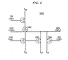
- FIG. 5 A schematic diagram of the row termination clock gate circuit is shown in FIG. 5.
- two such circuits are used to steer the row termination clock signal CRTD to the row clock generator associated with the partially selected sub-array.
- the output of each circuit CRTU or CRTL is maintained at VSS owing to PRO being a "high” logic level.
- PRO which is initiated by the row enable signal going "low” causes transistor 5001 to become nonconducting.
- the state of column address bit CA8 is such that transistor 5002 is in its nonconducting state when row termination clock signal CRTD goes "high".
- FIG. 6 there is shown a schematic diagram of a row decoder interrupt clock generator circuit.
- the preferred embodiment includes two such circuits, one associated with each sub-array. The inputs and the output of the circuit associated with the lower sub-array are enclosed in parentheses.
- the output of each circuit CRDIBU or CRDIBL is at a boosted potential of greater than VDD + VT.
- the row address buffer precharge clock signal PRA Shortly after the row clock signals CRU and CRL go “high” the row address buffer precharge clock signal PRA also goes “high” to cause the outputs of both circuits to go “low”.
- the row clock termination gates CRTU and CRTL allow the row terminate clock signal to be applied to only the circuit associated with the partially selected sub-array. Therefore, when the row terminate clock signal goes "high” the output of the circuit associated with the partially selected sub-array returns to a boosted "high” logic level. The output of the circuit associated with the fully selected sub-array remains at a "low” logic level until the master row precharge clock PRO returns "high” at the end of the operating cycle.
- Illustrative waveforms representing typical behaviour of the signals at the inputs and the output of the row decoder interrupt generator circuits are included in FIG. 5. The waveforms illustrate the case in which the upper sub-array is fully selected.
- FIG. 7 there is shown a schematic diagram of the column precharge clock circuit.
- Two such circuits are included in the preferred embodiment, one associated with each sub-array.
- the inputs and the output of the circuit associated with the lower sub-array are enclosed in parentheses.
- the output PCBU or PCBL of each circuit is at a boosted "high” logic level of greater than VDD + VT.
- the row address bit RAO goes “high”
- the output of each circuit goes “low”.
- the output of each circuit returns to a "high” logic level when the corresponding row decoder interrupts clock signal CRDIBU or CRDIBL goes “high”.
- the row decoder interrupt clock signal associated with the partially selected sub-array goes "high” before that associated with the fully selected sub-array. Therefore, the output of the column precharge circuit associated with the partially selected sub-array returns to the "high" logic level before that of the circuit associated with the fully selected sub-array.
- Illustrative waveforms representing typical behaviour of the signals at the inputs and the output of the column precharge clock generator circuits are included in FIG. 7 for the case in which the upper sub-array is fully selected.
Landscapes
- Engineering & Computer Science (AREA)
- Microelectronics & Electronic Packaging (AREA)
- Computer Hardware Design (AREA)
- Dram (AREA)
Applications Claiming Priority (2)
| Application Number | Priority Date | Filing Date | Title |
|---|---|---|---|
| US06/010,741 US4222112A (en) | 1979-02-09 | 1979-02-09 | Dynamic RAM organization for reducing peak current |
| US10741 | 1979-02-09 |
Publications (3)
| Publication Number | Publication Date |
|---|---|
| EP0023510A1 EP0023510A1 (en) | 1981-02-11 |
| EP0023510A4 EP0023510A4 (en) | 1982-09-03 |
| EP0023510B1 true EP0023510B1 (en) | 1984-12-05 |
Family
ID=21747181
Family Applications (1)
| Application Number | Title | Priority Date | Filing Date |
|---|---|---|---|
| EP80900356A Expired EP0023510B1 (en) | 1979-02-09 | 1980-08-25 | Memory organization for reducing peak current |
Country Status (6)
| Country | Link |
|---|---|
| US (1) | US4222112A (enExample) |
| EP (1) | EP0023510B1 (enExample) |
| JP (1) | JPS6336079B2 (enExample) |
| CA (1) | CA1127762A (enExample) |
| DE (1) | DE3069730D1 (enExample) |
| WO (1) | WO1980001731A1 (enExample) |
Families Citing this family (26)
| Publication number | Priority date | Publication date | Assignee | Title |
|---|---|---|---|---|
| US4556961A (en) * | 1981-05-26 | 1985-12-03 | Tokyo Shibaura Denki Kabushiki Kaisha | Semiconductor memory with delay means to reduce peak currents |
| JPS589285A (ja) * | 1981-07-08 | 1983-01-19 | Toshiba Corp | 半導体装置 |
| JPS5819793A (ja) * | 1981-07-27 | 1983-02-04 | Toshiba Corp | 半導体メモリ装置 |
| JPS58121195A (ja) * | 1982-01-13 | 1983-07-19 | Nec Corp | プリチヤ−ジ信号発生回路 |
| JPS58211393A (ja) * | 1982-06-02 | 1983-12-08 | Mitsubishi Electric Corp | 半導体メモリ装置 |
| EP0162934B1 (de) * | 1984-05-14 | 1989-11-08 | Ibm Deutschland Gmbh | Halbleiterspeicher |
| JPS618796A (ja) * | 1984-06-20 | 1986-01-16 | Nec Corp | ダイナミツクメモリ |
| JPS6177198A (ja) * | 1984-09-21 | 1986-04-19 | Toshiba Corp | 半導体記憶装置 |
| US4663742A (en) * | 1984-10-30 | 1987-05-05 | International Business Machines Corporation | Directory memory system having simultaneous write, compare and bypass capabilites |
| US4656612A (en) * | 1984-11-19 | 1987-04-07 | Inmos Corporation | Dram current control technique |
| US4636990A (en) * | 1985-05-31 | 1987-01-13 | International Business Machines Corporation | Three state select circuit for use in a data processing system or the like |
| JPH0778993B2 (ja) * | 1985-11-05 | 1995-08-23 | 株式会社日立製作所 | 半導体メモリ |
| EP0293933B1 (en) * | 1987-06-04 | 1993-10-13 | Nec Corporation | Dynamic memory circuit with improved sensing scheme |
| US4845677A (en) * | 1987-08-17 | 1989-07-04 | International Business Machines Corporation | Pipelined memory chip structure having improved cycle time |
| KR910002034B1 (ko) * | 1988-07-21 | 1991-03-30 | 삼성전자 주식회사 | 다분할형 메모리 어레이의 충전등화회로 |
| DE4008496C2 (de) * | 1989-03-16 | 1994-11-10 | Mitsubishi Electric Corp | Halbleiterspeichereinrichtung und Verfahren zum Treiben von Leseverstärkereinrichtungen |
| US5276649A (en) * | 1989-03-16 | 1994-01-04 | Mitsubishi Denki Kabushiki Kaisha | Dynamic-type semiconductor memory device having staggered activation of column groups |
| IL96808A (en) * | 1990-04-18 | 1996-03-31 | Rambus Inc | Introductory / Origin Circuit Agreed Using High-Performance Brokerage |
| JPH04109488A (ja) * | 1990-08-29 | 1992-04-10 | Mitsubishi Electric Corp | ダイナミック型半導体記憶装置 |
| DE4422784C2 (de) * | 1994-06-29 | 1999-05-27 | Texas Instruments Deutschland | Schaltungsanordnung mit wenigstens einer Schaltungseinheit wie einem Register, einer Speicherzelle, einer Speicheranordnung oder dergleichen |
| DE10041688B4 (de) * | 2000-08-24 | 2008-03-27 | Infineon Technologies Ag | Integrierter Speicher mit Speicherzellen in mehreren Speicherzellenblöcken und Verfahren zum Betrieb eines solchen Speichers |
| KR100539964B1 (ko) * | 2003-06-27 | 2005-12-28 | 주식회사 하이닉스반도체 | 반도체 메모리 소자의 프리차지 장치 및 이를 이용한 프리차지 방법 |
| US7200062B2 (en) | 2004-08-31 | 2007-04-03 | Micron Technology, Inc. | Method and system for reducing the peak current in refreshing dynamic random access memory devices |
| JP5084134B2 (ja) | 2005-11-21 | 2012-11-28 | 日本電気株式会社 | 表示装置及びこれらを用いた機器 |
| US8310893B2 (en) * | 2009-12-16 | 2012-11-13 | Micron Technology, Inc. | Techniques for reducing impact of array disturbs in a semiconductor memory device |
| US20250147875A1 (en) * | 2023-11-07 | 2025-05-08 | Rambus Inc. | Memory device with staggered access |
Family Cites Families (5)
| Publication number | Priority date | Publication date | Assignee | Title |
|---|---|---|---|---|
| US3866061A (en) * | 1973-08-27 | 1975-02-11 | Burroughs Corp | Overlap timing control circuit for conditioning signals in a semiconductor memory |
| JPS52119160A (en) * | 1976-03-31 | 1977-10-06 | Nec Corp | Semiconductor circuit with insulating gate type field dffect transisto r |
| JPS6030039B2 (ja) * | 1977-02-25 | 1985-07-13 | 株式会社東芝 | 半導体ダイナミツクメモリ装置 |
| JPS6034192B2 (ja) * | 1977-04-18 | 1985-08-07 | 株式会社日立製作所 | メモリ |
| US4162540A (en) * | 1978-03-20 | 1979-07-24 | Fujitsu Limited | Clocked memory with delay establisher by drive transistor design |
-
1979
- 1979-02-09 US US06/010,741 patent/US4222112A/en not_active Expired - Lifetime
-
1980
- 1980-01-28 JP JP55500481A patent/JPS6336079B2/ja not_active Expired
- 1980-01-28 WO PCT/US1980/000074 patent/WO1980001731A1/en not_active Ceased
- 1980-01-28 DE DE8080900356T patent/DE3069730D1/de not_active Expired
- 1980-02-07 CA CA345,195A patent/CA1127762A/en not_active Expired
- 1980-08-25 EP EP80900356A patent/EP0023510B1/en not_active Expired
Non-Patent Citations (2)
| Title |
|---|
| Electronics, vol. 49, no. 10, 13 May 1976 NEW YORK (US) C. KUO et al : "16-K RAM built with proven process may offer high start-up reliability" * |
| Patents Abstracts of Japan, vol. 1, no. 155, 12 December 1977 page 8307E77 * |
Also Published As
| Publication number | Publication date |
|---|---|
| CA1127762A (en) | 1982-07-13 |
| EP0023510A4 (en) | 1982-09-03 |
| JPS56500231A (enExample) | 1981-02-26 |
| WO1980001731A1 (en) | 1980-08-21 |
| JPS6336079B2 (enExample) | 1988-07-19 |
| EP0023510A1 (en) | 1981-02-11 |
| DE3069730D1 (en) | 1985-01-17 |
| US4222112A (en) | 1980-09-09 |
Similar Documents
| Publication | Publication Date | Title |
|---|---|---|
| EP0023510B1 (en) | Memory organization for reducing peak current | |
| US4542483A (en) | Dual stage sense amplifier for dynamic random access memory | |
| US4768171A (en) | Memory circuit having a plurality of cell arrays | |
| KR930001554B1 (ko) | 다이나믹 반도체 기억장치와 그 구동방법 | |
| US4817057A (en) | Semiconductor memory device having improved precharge scheme | |
| US5091885A (en) | Dynamic type random-access memory having improved timing characteristics | |
| GB1566221A (en) | Integrated circuit for random access memory chip | |
| US4241425A (en) | Organization for dynamic random access memory | |
| US4533843A (en) | High performance dynamic sense amplifier with voltage boost for row address lines | |
| EP0316902B1 (en) | Semiconductor memory circuit having an improved restoring scheme | |
| US6137737A (en) | Method and circuit for rapidly equilibrating paired digit lines of a memory device during testing | |
| US4748349A (en) | High performance dynamic sense amplifier with voltage boost for row address lines | |
| US5361233A (en) | Semiconductor memory apparatus | |
| US4543500A (en) | High performance dynamic sense amplifier voltage boost for row address lines | |
| US5323345A (en) | Semiconductor memory device having read/write circuitry | |
| EP0373672B1 (en) | Semiconductor memory circuit having an improved restoring control circuit | |
| US5295111A (en) | Dynamic random access memory device with improved power supply system for speed-up of rewriting operation on data bits read-out from memory cells | |
| JPH0223958B2 (enExample) | ||
| US5430686A (en) | Semiconductor memory device and operating method thereof | |
| KR960000891B1 (ko) | 데이타 읽어내기 완료 타이밍을 빠르게한 다이내믹 ram | |
| EP0166642A2 (en) | Block-divided semiconductor memory device having divided bit lines | |
| WO1985002314A2 (en) | Semiconductor memory | |
| JP2698232B2 (ja) | 半導体記憶装置 | |
| US4327426A (en) | Column decoder discharge for semiconductor memory | |
| JPH054753B2 (enExample) |
Legal Events
| Date | Code | Title | Description |
|---|---|---|---|
| PUAI | Public reference made under article 153(3) epc to a published international application that has entered the european phase |
Free format text: ORIGINAL CODE: 0009012 |
|
| AK | Designated contracting states |
Designated state(s): DE FR GB NL |
|
| 17P | Request for examination filed |
Effective date: 19810212 |
|
| GRAA | (expected) grant |
Free format text: ORIGINAL CODE: 0009210 |
|
| AK | Designated contracting states |
Designated state(s): DE FR GB NL |
|
| REF | Corresponds to: |
Ref document number: 3069730 Country of ref document: DE Date of ref document: 19850117 |
|
| ET | Fr: translation filed | ||
| PLBE | No opposition filed within time limit |
Free format text: ORIGINAL CODE: 0009261 |
|
| STAA | Information on the status of an ep patent application or granted ep patent |
Free format text: STATUS: NO OPPOSITION FILED WITHIN TIME LIMIT |
|
| 26N | No opposition filed | ||
| PGFP | Annual fee paid to national office [announced via postgrant information from national office to epo] |
Ref country code: NL Payment date: 19890131 Year of fee payment: 13 |
|
| PGFP | Annual fee paid to national office [announced via postgrant information from national office to epo] |
Ref country code: DE Payment date: 19891220 Year of fee payment: 11 |
|
| PGFP | Annual fee paid to national office [announced via postgrant information from national office to epo] |
Ref country code: FR Payment date: 19891221 Year of fee payment: 11 |
|
| PGFP | Annual fee paid to national office [announced via postgrant information from national office to epo] |
Ref country code: GB Payment date: 19891231 Year of fee payment: 11 |
|
| PG25 | Lapsed in a contracting state [announced via postgrant information from national office to epo] |
Ref country code: GB Effective date: 19910128 |
|
| PG25 | Lapsed in a contracting state [announced via postgrant information from national office to epo] |
Ref country code: NL Effective date: 19910801 |
|
| NLV4 | Nl: lapsed or anulled due to non-payment of the annual fee | ||
| GBPC | Gb: european patent ceased through non-payment of renewal fee | ||
| PG25 | Lapsed in a contracting state [announced via postgrant information from national office to epo] |
Ref country code: FR Effective date: 19910930 |
|
| PG25 | Lapsed in a contracting state [announced via postgrant information from national office to epo] |
Ref country code: DE Effective date: 19911001 |
|
| REG | Reference to a national code |
Ref country code: FR Ref legal event code: ST |