CN112655282A - 带有端子的电路基板和电路基板组件 - Google Patents
带有端子的电路基板和电路基板组件 Download PDFInfo
- Publication number
- CN112655282A CN112655282A CN201980051922.6A CN201980051922A CN112655282A CN 112655282 A CN112655282 A CN 112655282A CN 201980051922 A CN201980051922 A CN 201980051922A CN 112655282 A CN112655282 A CN 112655282A
- Authority
- CN
- China
- Prior art keywords
- circuit board
- sub
- terminal
- board
- substrate
- Prior art date
- Legal status (The legal status is an assumption and is not a legal conclusion. Google has not performed a legal analysis and makes no representation as to the accuracy of the status listed.)
- Pending
Links
- 239000004020 conductor Substances 0.000 claims abstract description 24
- 239000000758 substrate Substances 0.000 claims description 55
- 238000003466 welding Methods 0.000 claims description 2
- 238000007772 electroless plating Methods 0.000 description 4
- 238000005476 soldering Methods 0.000 description 4
- 238000000034 method Methods 0.000 description 3
- 230000000694 effects Effects 0.000 description 1
- 229910000679 solder Inorganic materials 0.000 description 1
Images
Classifications
-
- H—ELECTRICITY
- H01—ELECTRIC ELEMENTS
- H01R—ELECTRICALLY-CONDUCTIVE CONNECTIONS; STRUCTURAL ASSOCIATIONS OF A PLURALITY OF MUTUALLY-INSULATED ELECTRICAL CONNECTING ELEMENTS; COUPLING DEVICES; CURRENT COLLECTORS
- H01R12/00—Structural associations of a plurality of mutually-insulated electrical connecting elements, specially adapted for printed circuits, e.g. printed circuit boards [PCB], flat or ribbon cables, or like generally planar structures, e.g. terminal strips, terminal blocks; Coupling devices specially adapted for printed circuits, flat or ribbon cables, or like generally planar structures; Terminals specially adapted for contact with, or insertion into, printed circuits, flat or ribbon cables, or like generally planar structures
- H01R12/70—Coupling devices
- H01R12/71—Coupling devices for rigid printing circuits or like structures
- H01R12/72—Coupling devices for rigid printing circuits or like structures coupling with the edge of the rigid printed circuits or like structures
- H01R12/722—Coupling devices for rigid printing circuits or like structures coupling with the edge of the rigid printed circuits or like structures coupling devices mounted on the edge of the printed circuits
- H01R12/724—Coupling devices for rigid printing circuits or like structures coupling with the edge of the rigid printed circuits or like structures coupling devices mounted on the edge of the printed circuits containing contact members forming a right angle
-
- H—ELECTRICITY
- H01—ELECTRIC ELEMENTS
- H01Q—ANTENNAS, i.e. RADIO AERIALS
- H01Q1/00—Details of, or arrangements associated with, antennas
- H01Q1/36—Structural form of radiating elements, e.g. cone, spiral, umbrella; Particular materials used therewith
- H01Q1/38—Structural form of radiating elements, e.g. cone, spiral, umbrella; Particular materials used therewith formed by a conductive layer on an insulating support
-
- H—ELECTRICITY
- H01—ELECTRIC ELEMENTS
- H01Q—ANTENNAS, i.e. RADIO AERIALS
- H01Q9/00—Electrically-short antennas having dimensions not more than twice the operating wavelength and consisting of conductive active radiating elements
- H01Q9/04—Resonant antennas
- H01Q9/30—Resonant antennas with feed to end of elongated active element, e.g. unipole
- H01Q9/42—Resonant antennas with feed to end of elongated active element, e.g. unipole with folded element, the folded parts being spaced apart a small fraction of the operating wavelength
-
- H—ELECTRICITY
- H01—ELECTRIC ELEMENTS
- H01R—ELECTRICALLY-CONDUCTIVE CONNECTIONS; STRUCTURAL ASSOCIATIONS OF A PLURALITY OF MUTUALLY-INSULATED ELECTRICAL CONNECTING ELEMENTS; COUPLING DEVICES; CURRENT COLLECTORS
- H01R12/00—Structural associations of a plurality of mutually-insulated electrical connecting elements, specially adapted for printed circuits, e.g. printed circuit boards [PCB], flat or ribbon cables, or like generally planar structures, e.g. terminal strips, terminal blocks; Coupling devices specially adapted for printed circuits, flat or ribbon cables, or like generally planar structures; Terminals specially adapted for contact with, or insertion into, printed circuits, flat or ribbon cables, or like generally planar structures
- H01R12/70—Coupling devices
- H01R12/71—Coupling devices for rigid printing circuits or like structures
- H01R12/712—Coupling devices for rigid printing circuits or like structures co-operating with the surface of the printed circuit or with a coupling device exclusively provided on the surface of the printed circuit
- H01R12/716—Coupling device provided on the PCB
-
- H—ELECTRICITY
- H05—ELECTRIC TECHNIQUES NOT OTHERWISE PROVIDED FOR
- H05K—PRINTED CIRCUITS; CASINGS OR CONSTRUCTIONAL DETAILS OF ELECTRIC APPARATUS; MANUFACTURE OF ASSEMBLAGES OF ELECTRICAL COMPONENTS
- H05K1/00—Printed circuits
- H05K1/02—Details
- H05K1/14—Structural association of two or more printed circuits
- H05K1/141—One or more single auxiliary printed circuits mounted on a main printed circuit, e.g. modules, adapters
-
- H—ELECTRICITY
- H05—ELECTRIC TECHNIQUES NOT OTHERWISE PROVIDED FOR
- H05K—PRINTED CIRCUITS; CASINGS OR CONSTRUCTIONAL DETAILS OF ELECTRIC APPARATUS; MANUFACTURE OF ASSEMBLAGES OF ELECTRICAL COMPONENTS
- H05K3/00—Apparatus or processes for manufacturing printed circuits
- H05K3/36—Assembling printed circuits with other printed circuits
- H05K3/366—Assembling printed circuits with other printed circuits substantially perpendicularly to each other
-
- H—ELECTRICITY
- H05—ELECTRIC TECHNIQUES NOT OTHERWISE PROVIDED FOR
- H05K—PRINTED CIRCUITS; CASINGS OR CONSTRUCTIONAL DETAILS OF ELECTRIC APPARATUS; MANUFACTURE OF ASSEMBLAGES OF ELECTRICAL COMPONENTS
- H05K1/00—Printed circuits
- H05K1/16—Printed circuits incorporating printed electric components, e.g. printed resistor, capacitor, inductor
- H05K1/165—Printed circuits incorporating printed electric components, e.g. printed resistor, capacitor, inductor incorporating printed inductors
-
- H—ELECTRICITY
- H05—ELECTRIC TECHNIQUES NOT OTHERWISE PROVIDED FOR
- H05K—PRINTED CIRCUITS; CASINGS OR CONSTRUCTIONAL DETAILS OF ELECTRIC APPARATUS; MANUFACTURE OF ASSEMBLAGES OF ELECTRICAL COMPONENTS
- H05K2201/00—Indexing scheme relating to printed circuits covered by H05K1/00
- H05K2201/04—Assemblies of printed circuits
- H05K2201/048—Second PCB mounted on first PCB by inserting in window or holes of the first PCB
-
- H—ELECTRICITY
- H05—ELECTRIC TECHNIQUES NOT OTHERWISE PROVIDED FOR
- H05K—PRINTED CIRCUITS; CASINGS OR CONSTRUCTIONAL DETAILS OF ELECTRIC APPARATUS; MANUFACTURE OF ASSEMBLAGES OF ELECTRICAL COMPONENTS
- H05K2201/00—Indexing scheme relating to printed circuits covered by H05K1/00
- H05K2201/10—Details of components or other objects attached to or integrated in a printed circuit board
- H05K2201/10007—Types of components
- H05K2201/10098—Components for radio transmission, e.g. radio frequency identification [RFID] tag, printed or non-printed antennas
Landscapes
- Engineering & Computer Science (AREA)
- Microelectronics & Electronic Packaging (AREA)
- Manufacturing & Machinery (AREA)
- Combinations Of Printed Boards (AREA)
- Coupling Device And Connection With Printed Circuit (AREA)
- Multi-Conductor Connections (AREA)
- Parts Printed On Printed Circuit Boards (AREA)
- Printing Elements For Providing Electric Connections Between Printed Circuits (AREA)
- Details Of Aerials (AREA)
Abstract
提供能够使电路基板的端部作为端子而使用、并且还能够作为宽度狭小的端子而使用的带有端子的电路基板和电路基板组件。第一子基板(20)具有从其侧端面(23)、下端面(25)与第一子基板(20)的正、背面齐平地拥有第一子基板(20)的厚度而突出的端子部(24,26)。而且,在这些端子部(24,26)的与第一子基板(20)的正、背面齐平的第一面和第二面进而加上与第一面和第二面相交的两个侧面的四个面,遍及一周由导电性材料的膜覆盖。
Description
技术领域
本发明涉及带有端子的电路基板和装配了多块电路基板的电路基板组件。
背景技术
在将电路零件搭载于电路基板时,将电路零件的针脚形状的端子插入在内壁表面镀有导电性材料的通孔,在通孔内焊接的搭载方法被广泛采用。
即使在将电路基板搭载于另一电路基板时,也能考虑适用上述的搭载方法。即,能考虑将针脚形状的端子通过焊接等固定于一个电路基板,在另一个电路基板形成通孔,将端子插入通孔而焊接连接。然而,该连接结构需要与电路基板分开的端子,因而有成本变高的风险。
在此,在专利文献1中公开了将第一电路基板的端部插入第二电路基板的贯通孔的连接结构。在专利文献1的连接结构的情况下,能够焊接的表面仅为第一电路基板的正面和背面两个面,因而有焊接变得不充分的风险。
于是,考虑在上述的专利文献1所公开的连接结构中适用将端子插入通孔而焊接的上述搭载方法。即,在第二电路基板的贯通孔的内壁表面镀导电性材料,将第一电路基板的端部视作端子而将该端部插入贯通孔,在贯通孔内焊接。若采用该方式,则不需要与电路基板分开的端子,因而能够降低成本。
在此,对插入通孔的类型的端子的标准,有被要求遍及通孔内壁表面的75%以上而焊接。因此,如果要利用电路基板的正面和背面两个面的导电性材料来满足该标准,则需要使该端子的左右端面的面积为不满该端子整周的面积的25%,或者安全起见而比其更进一步减小面积比例。这即意味着,需要为沿电路基板的正、背面延伸较长的端子。在这种情况下,将多个端子以小间距排列是不可能的,不能够适用于这样的用途。另外,在将包含端子而需要使阻抗匹配的电路,例如天线图案等形成或搭载于电路基板上的情况下,有在延伸较长的端子中变得不能使阻抗匹配的风险。
现有技术文献
专利文献
专利文献1:日本特开2017-17089号公报。
发明内容
发明要解决的课题
本发明鉴于上述情形,目的在于提供能够使电路基板的端部作为端子而使用、并且还能够作为宽度狭小的端子而使用的带有端子的电路基板和电路基板组件。
用于解决课题的方案
达成上述目的的本发明的带有端子的电路基板,特征在于具有从电路基板的端面与电路基板的正、背面齐平地拥有电路基板厚度而突出的端子部,在上述端子部的与电路基板的正、背面齐平的第一面和第二面进而加上与第一面和第二面相交的两个侧面的四个面由导电性材料覆盖。
本发明的带有端子的电路基板不仅端子部的正、背两个面,两个侧面也由导电性材料覆盖。因此,遍及对方基板的通孔内壁表面的整周被焊接。进而,能够为满足上述标准且宽度狭小的端子。
在此,本发明的带有端子的电路基板还可以在电路基板的正、背面中的至少一个具有天线图案。
即便在具有天线图案的电路基板的情况下,也能够为使阻抗与该天线图案匹配的端子。
另外,在本发明的带有端子的电路基板中,优选地,除了端子部的上述四个面之外,进而端子部的突出的前端的第五面由导电性材料覆盖。
另外,达成上述目的的本发明的电路基板组件,特征在于具备为本发明的任一方式的带有端子的电路基板的第一电路基板、和具有内壁表面整个周面由导电性材料覆盖的通孔的第二电路基板,上述端子部插入上述通孔,通孔的内壁表面和端子部的遍及整周的四个面被焊接连接。
发明效果
依据以上的本发明,能够使电路基板的端部作为插入通孔而焊接的宽度狭小的端子而利用。
附图说明
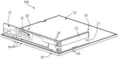
图1是作为本发明的一个实施方式的电路基板组件的立体图。
图2是示出装配前的第一子基板和第二子基板的分解立体图。
图3是示出装配状态下的第一子基板和第二子基板的立体图。
图4是示出母基板和装配状态下的第一子基板和第二子基板的分解立体图。
具体实施方式
以下,对本发明的实施方式进行说明。
图1是作为本发明的一个实施方式的电路基板组件的立体图。
该电路基板组件100具备主基板(母基板)10、第一子基板20和第二子基板30这三块电路基板。
在第一子基板20的正面21,形成有构成主要在第二子基板30的正面31形成的天线图案32的一部分的电路图案22。该电路图案22介由两个端子部24中的一个耦接至第二子基板30上的天线图案32。
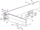
图2是示出装配前的第一子基板和第二子基板的分解立体图。
另外,图3是示出装配状态下的第一子基板和第二子基板的立体图。
在第二子基板30侧的第一子基板20设有两个端子部24。这些端子部24具有从第一子基板20的侧端面23与第一子基板20的正、背面齐平地拥有第一子基板20的厚度而突出的形状。
在这些端子部24的与第一子基板20的正面21齐平的第一面241和与第一子基板20的背面齐平的未图示的第二面,形成有导电性材料的膜。另外,端子部24的与第一面241和第二面相交的两个侧面也由导电性材料的膜覆盖。该两个侧面的膜是通过与向通孔的内壁表面的无电镀相同的无电镀的手段形成的。进而,端子部24的从第一子基板20突出的前端的端面242也可以由导电性材料的膜覆盖。该前端的端面242与本发明所述的第五面的一个示例相当。
另一方面,在第二子基板30,设有第一子基板20的两个端子部24中的各个所插入的纵长的两个通孔34。这些通孔34的内壁表面通过无电镀遍及其整个周面由导电性材料的膜覆盖。
在第一子基板20与第二子基板30装配时,将第一子基板20的两个端子部24分别插入第二子基板30的两个通孔34。在该状态下,将端子部24与通孔34的内壁表面之间焊接连接。端子部24遍及其整周的四个面由导电性材料的膜覆盖,因而遍及其整周被焊接。
在该第一子基板20与第二子基板30的关系中,第一子基板20与本发明的带有端子的电路基板(第一电路基板)的一个示例相当。另外,第二子基板30与本发明所述的第二电路基板的一个示例相当。而且,这些第一子基板20与第二子基板30的组合与本发明的电路基板组件的一个示例相当。
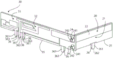
另外,第一子基板20具备从该第一子基板20的下端面25向下突出的另一个端子部26。该端子部26也具有与第一子基板20的正、背面齐平地拥有第一子基板20的厚度而突出的形状。而且,该端子部26中,与第一子基板20的正面21齐平的第一面261和为其背面的第二面(未图示)由导电性材料的膜覆盖。另外,该端子部26中,与其第一面261和第二面相交的两个侧面也由导电性材料的膜覆盖。即,该端子部26也与端子部24同样地,遍及一周,即在第一面261和第二面进而加上两个侧面的四个面由导电性材料的膜覆盖。此外,端子部26也与端子部24同样地,从第一子基板20突出的前端的端面262也可以由导电性材料的膜覆盖。在这种情况下,能够进一步形成良好形状的焊角。该前端的端面262与本发明所述的第五面的一个示例相当。
进而,第二子基板30形成有从该第二子基板30的下端面35向下突出的四个端子部36(参照图3),其中的三个依次接近而排列。这些端子部36也具有与第二子基板30的正、背面齐平地拥有第二子基板30的厚度而突出的形状。而且,该端子部36的与第二子基板30的正面31和背面39分别齐平的第一面361和第二面362由导电性材料的膜覆盖。进而,该端子部36的与其第一面361和第二面362相交的两个侧面也由导电性材料的膜覆盖。即,该端子部36也与形成于第一子基板20的端子部24、26同样地,遍及一周,即在第一面361和第二面362进而加上两个侧面的四个面由导电性材料的膜覆盖。此外,端子部36也与端子部24、26同样地,从第二子基板30突出的前端的端面363也可以由导电性材料的膜覆盖。端面363与本发明所述的第五面的一个示例相当。
这些第一子基板20和第二子基板30的向下突出的端子部26、36是用于如图3所示地将被装配为L字形状的第一子基板20和第二子基板30焊接连接于母基板10的端子部。
第二子基板30的向下突出的四个端子部36中的排列而形成的三个端子部36耦接至天线图案32。而且,这三个端子部36中的各个成为阻抗与天线图案32匹配的尺寸的端子部。
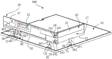
图4是示出母基板和装配状态下的第一子基板和第二子基板的分解立体图。
在母基板10,形成有第一子基板20的向下突出的端子部26所插入的通孔11。另外,在母基板10,形成有第二子基板30的向下突出的四个端子部36所插入的四个通孔12。这些通孔11、12中的各个的内壁表面,其整周由通过无电镀形成的导电性材料的膜覆盖。而且,各端子部26、36插入各通孔11、12而被焊接。图1示出了第一子基板20和第二子基板30以此方式搭载于母基板10的状态。
在此,在母基板10与装配状态下的第一子基板20和第二子基板30的关系中,装配状态下的第一子基板20和第二子基板30与本发明的带有端子的电路基板的一个示例,即本发明所述的第一电路基板的一个示例相当。另外,在这种情况下,母基板10与本发明所述的第二电路基板的一个示例相当。而且,装配状态下的第一子基板20和第二子基板30与母基板10的组合与本发明的电路基板组件的一个示例相当。
此外,在此举例说明了形成有天线图案的电路基板,但本发明也能够适用于不具有天线图案的电路基板。
另外,在此举例说明了L字形状的子基板与母基板的组合,但本发明不限于该组合,能够在装配电路基板彼此时广泛采用。
符号说明
10 母基板
11、12 通孔
20 第一子基板
21 正面
22 电路图案
23 侧端面
24 端子部
241 第一面
242 端面
25 下端面
26 端子部
261 第一面
262 端面
30 第二子基板
31 正面
32 天线图案
34 通孔
35 下端面
36 端子部
361 第一面
362 第二面
363 端面
39 背面
100 电路基板组件。
Claims (4)
1.一种带有端子的电路基板,其特征在于,
具有从电路基板的端面与该电路基板的正、背面齐平地拥有该电路基板的厚度而突出的端子部,
在所述端子部的与所述电路基板的正、背面齐平的第一面和第二面进而加上与该第一面和该第二面相交的两个侧面的四个面由导电性材料覆盖。
2.根据权利要求1所述的带有端子的电路基板,其特征在于,在所述正、背面中的至少一个具有天线图案。
3.根据权利要求1或2所述的带有端子的电路基板,其特征在于,除了所述端子部的所述四个面之外,进而该端子部的突出的前端的第五面由导电性材料覆盖。
4. 一种电路基板组件,其特征在于,具备:
为权利要求1至3中的任一项所述的带有端子的电路基板的第一电路基板;和
具有内壁表面整个周面由导电性材料覆盖的通孔的第二电路基板,
所述端子部插入所述通孔,所述内壁表面和所述四个面被焊接连接。
Applications Claiming Priority (3)
| Application Number | Priority Date | Filing Date | Title |
|---|---|---|---|
| JP2018148540A JP7210186B2 (ja) | 2018-08-07 | 2018-08-07 | 回路基板組立体 |
| JP2018-148540 | 2018-08-07 | ||
| PCT/JP2019/026993 WO2020031584A1 (ja) | 2018-08-07 | 2019-07-08 | 端子付き回路基板および回路基板組立体 |
Publications (1)
| Publication Number | Publication Date |
|---|---|
| CN112655282A true CN112655282A (zh) | 2021-04-13 |
Family
ID=69413745
Family Applications (1)
| Application Number | Title | Priority Date | Filing Date |
|---|---|---|---|
| CN201980051922.6A Pending CN112655282A (zh) | 2018-08-07 | 2019-07-08 | 带有端子的电路基板和电路基板组件 |
Country Status (5)
| Country | Link |
|---|---|
| US (1) | US11664615B2 (zh) |
| EP (1) | EP3836763A4 (zh) |
| JP (1) | JP7210186B2 (zh) |
| CN (1) | CN112655282A (zh) |
| WO (1) | WO2020031584A1 (zh) |
Families Citing this family (3)
| Publication number | Priority date | Publication date | Assignee | Title |
|---|---|---|---|---|
| JP6947657B2 (ja) * | 2018-01-31 | 2021-10-13 | 株式会社デンソー | 電子回路 |
| JP2022178257A (ja) | 2021-05-19 | 2022-12-02 | タイコエレクトロニクスジャパン合同会社 | 回路基板組立体 |
| US20230076176A1 (en) * | 2021-09-08 | 2023-03-09 | Rohde & Schwarz Gmbh & Co. Kg | Circuit board arrangement, differential probe circuit and method |
Citations (4)
| Publication number | Priority date | Publication date | Assignee | Title |
|---|---|---|---|---|
| US20090213562A1 (en) * | 2008-02-27 | 2009-08-27 | Julian Thevenard | System for interconnecting two substrates each comprising at least one transmission line |
| CN102105017A (zh) * | 2009-12-17 | 2011-06-22 | 松下电工株式会社 | 印制布线板连接构造 |
| JP2011222826A (ja) * | 2010-04-12 | 2011-11-04 | Mitsubishi Electric Engineering Co Ltd | プリント基板間の接続構造 |
| CN108184333A (zh) * | 2015-11-05 | 2018-06-19 | 阿莫技术有限公司 | 组合式天线模块 |
Family Cites Families (61)
| Publication number | Priority date | Publication date | Assignee | Title |
|---|---|---|---|---|
| DE2013258C3 (de) * | 1970-03-20 | 1975-05-22 | Standard Elektrik Lorenz Ag, 7000 Stuttgart | Verfahren zur Herstellung von stiftförmigen Anschlußteilen einer gedruckten Schaltungsplatte |
| JPS534146Y2 (zh) | 1973-02-21 | 1978-02-01 | ||
| JPS558953Y2 (zh) * | 1975-04-04 | 1980-02-27 | ||
| JPS5493455A (en) | 1977-12-30 | 1979-07-24 | Matsushita Electric Works Ltd | Printed circuit board for small electronic appliance |
| JPS5996874U (ja) | 1982-12-21 | 1984-06-30 | オムロン株式会社 | 電子機器の組立構造 |
| JPH02132970A (ja) | 1988-11-14 | 1990-05-22 | Sanyo Electric Co Ltd | 2値画像列中のデータ変化点の検出方法 |
| JPH02132970U (zh) * | 1989-04-11 | 1990-11-05 | ||
| US6239765B1 (en) * | 1999-02-27 | 2001-05-29 | Rangestar Wireless, Inc. | Asymmetric dipole antenna assembly |
| DE50002850D1 (de) * | 1999-05-31 | 2003-08-14 | Tyco Electronics Logistics Ag | Intelligentes leistungsmodul |
| WO2001047059A1 (en) * | 1999-12-23 | 2001-06-28 | Rangestar Wireless, Inc. | Dual polarization slot antenna assembly |
| US6824391B2 (en) * | 2000-02-03 | 2004-11-30 | Tyco Electronics Corporation | Electrical connector having customizable circuit board wafers |
| JP2001284761A (ja) | 2000-03-30 | 2001-10-12 | Omron Corp | プリント配線板固定装置と、このプリント配線板固定装置を用いた電子機器 |
| US6461169B1 (en) * | 2001-05-04 | 2002-10-08 | Intel Corporation | Interconnecting circuit modules to a motherboard using an edge connector with conductive polymer contacts |
| WO2003044891A1 (fr) * | 2001-11-20 | 2003-05-30 | Ube Industries, Ltd. | Module d'antenne dielectrique |
| US6808399B2 (en) * | 2002-12-02 | 2004-10-26 | Tyco Electronics Corporation | Electrical connector with wafers having split ground planes |
| KR100586698B1 (ko) * | 2003-12-23 | 2006-06-08 | 삼성전자주식회사 | 수직 실장된 반도체 칩 패키지를 갖는 반도체 모듈 |
| JP2005197493A (ja) | 2004-01-08 | 2005-07-21 | Ihi Aerospace Co Ltd | 回路基板組立体 |
| JP2005236089A (ja) | 2004-02-20 | 2005-09-02 | Matsushita Electric Ind Co Ltd | 三次元実装構造体、三次元実装構造体を備えた携帯用電子機器、および、三次元実装構造体の製造方法 |
| US6932649B1 (en) * | 2004-03-19 | 2005-08-23 | Tyco Electronics Corporation | Active wafer for improved gigabit signal recovery, in a serial point-to-point architecture |
| EP1729555B1 (de) * | 2005-05-31 | 2008-01-02 | Siemens Aktiengesellschaft | Verfahren zur Herstellung einer Leiterplatte und eines Leiterplattensystems sowie mittels solcher Verfahren hergestellte Leiterplattten und Leiterplattensysteme |
| JP2007068106A (ja) | 2005-09-02 | 2007-03-15 | Auto Network Gijutsu Kenkyusho:Kk | 車載用無線受信装置 |
| US7379021B2 (en) * | 2005-11-01 | 2008-05-27 | Arcadyan Technology Corporation | Circuit board |
| EP1804561B1 (en) * | 2005-12-30 | 2015-01-28 | Omron Europe B.V. | Printed circuit board for perpendicularly connecting electronic components |
| US7705365B2 (en) * | 2006-01-24 | 2010-04-27 | Denso Corporation | Lighting device and light emitting module for the same |
| US7338292B2 (en) * | 2006-01-26 | 2008-03-04 | Agilent Technologies, Inc. | Board-to-board electronic interface using hemi-ellipsoidal surface features |
| DE202006020076U1 (de) * | 2006-04-06 | 2007-10-04 | Behr-Hella Thermocontrol Gmbh | Leiterkartenanordnung |
| JP2008027869A (ja) | 2006-07-25 | 2008-02-07 | Jisedai Gijutsu:Kk | 基板コネクタ |
| AT504960B1 (de) * | 2007-01-31 | 2012-11-15 | Siemens Ag | Anordnung eines ersten schaltungsträgers auf einem zweiten schaltungsträger |
| US7864544B2 (en) * | 2007-08-01 | 2011-01-04 | Delphi Technologies, Inc. | Printed circuit board assembly |
| US7716821B2 (en) * | 2007-12-12 | 2010-05-18 | Sauer-Danfoss Inc. | Method of manufacturing a circuit board assembly for a controller |
| CN101752735B (zh) * | 2008-12-16 | 2012-08-29 | 鸿富锦精密工业(深圳)有限公司 | 板卡固定装置 |
| EP2401178B1 (en) * | 2009-02-27 | 2016-11-16 | Delphi Technologies, Inc. | Lightweight audio system for automotive applications and method |
| KR101675375B1 (ko) * | 2009-11-23 | 2016-11-14 | 삼성전자 주식회사 | 휴대단말기 내장용 pcb 안테나 |
| TWI417013B (zh) * | 2010-05-14 | 2013-11-21 | Kuang Hong Prec Co Ltd | 立體電路元件及其製作方法 |
| US8897032B2 (en) * | 2011-05-24 | 2014-11-25 | Xirrus, Inc. | Surface mount antenna contacts |
| WO2012171565A1 (de) * | 2011-06-16 | 2012-12-20 | Siemens Aktiengesellschaft | Elektrische kontakteinrichtung zur verbindung von leiterplatten |
| EP2544300A1 (en) * | 2011-07-08 | 2013-01-09 | Tyco Electronics Belgium EC BVBA | Printed antenna |
| JP2013219109A (ja) | 2012-04-05 | 2013-10-24 | Denso Corp | 基板組立体、およびこの基板組立体を用いた燃料性状センサ |
| US9252528B2 (en) * | 2013-07-02 | 2016-02-02 | Germane Systems, Llc | Printed circuit board, method of manufacturing same, and method of mounting the circuit board in a connector socket |
| JP2015082538A (ja) | 2013-10-22 | 2015-04-27 | 住友電装株式会社 | プリント基板およびプリント基板を備えた電子機器並びにプリント基板の製造方法 |
| JP6215068B2 (ja) * | 2014-01-28 | 2017-10-18 | 日本航空電子工業株式会社 | コネクタ |
| US9356366B2 (en) * | 2014-04-24 | 2016-05-31 | Tyco Electronics Corporation | Cable connector assembly for a communication system |
| JP6636460B2 (ja) * | 2014-05-22 | 2020-01-29 | シグニファイ ホールディング ビー ヴィSignify Holding B.V. | プリント回路基板アレンジメント及び主プリント回路基板に製品を取り付けるための方法 |
| CN105698037A (zh) * | 2014-11-25 | 2016-06-22 | 鸿富锦精密工业(深圳)有限公司 | 灯具 |
| US20160268034A1 (en) * | 2015-03-13 | 2016-09-15 | Bose Corporation | Planar Magnetic Components and Assemblies |
| BR112017022649B1 (pt) * | 2015-04-20 | 2022-09-06 | Interdigital Madison Patent Holdings, Sas | Dispositivo eletrônico, método de construção de um decodificador set-top box ou dispositivo de gateway tendo um invólucro e método de construção de uma submontagem para incorporar em uma pluralidade de decodificadores set-top box e dispositivos de gateway diferentes |
| JP2017017089A (ja) | 2015-06-29 | 2017-01-19 | 三菱電機株式会社 | 立体型プリント基板 |
| CA2941284C (en) * | 2015-09-08 | 2022-04-05 | Ross Video Limited | Circuit board pad layout and mechanical retainer |
| DE202015008007U1 (de) * | 2015-11-19 | 2016-01-11 | Siemens Aktiengesellschaft | Leiterplattenanordnung |
| JP6672737B2 (ja) | 2015-11-19 | 2020-03-25 | 三菱電機株式会社 | 調光器、照明システム |
| US9976898B2 (en) * | 2015-12-09 | 2018-05-22 | Pixart Imaging Inc. | Optical sensing module with multi-directional optical sensing function |
| DE202016101086U1 (de) * | 2016-03-01 | 2017-06-02 | Tridonic Gmbh & Co Kg | Leiterplattenanordnung |
| US10971880B2 (en) * | 2016-10-26 | 2021-04-06 | Neptune Technology Group Inc. | Connection for printed circuit board assemblies |
| JP6914583B2 (ja) | 2016-12-26 | 2021-08-04 | ダイハツ工業株式会社 | 車載用無線受信装置 |
| WO2019087352A1 (ja) * | 2017-11-02 | 2019-05-09 | 三菱電機株式会社 | プリント基板組立体 |
| EP3489082B1 (de) * | 2017-11-28 | 2021-10-06 | ZKW Group GmbH | Lichtmodul und fahrzeugscheinwerfer |
| JP6925447B2 (ja) * | 2017-12-08 | 2021-08-25 | 三菱電機株式会社 | プリント配線板およびその製造方法 |
| CA3107249C (en) * | 2018-07-26 | 2023-06-13 | Mitsubishi Electric Corporation | Printed circuit board |
| WO2020200464A1 (en) * | 2019-04-04 | 2020-10-08 | Huawei Technologies Co., Ltd. | Method for manufacturing an antenna element |
| DE102020104100B3 (de) * | 2020-02-17 | 2021-08-05 | Interplex NAS Electronics GmbH | Leiterkarten-Eckverbinder sowie Kartenverbindungsanordnung |
| US10998678B1 (en) * | 2020-03-26 | 2021-05-04 | TE Connectivity Services Gmbh | Modular electrical connector with additional grounding |
-
2018
- 2018-08-07 JP JP2018148540A patent/JP7210186B2/ja active Active
-
2019
- 2019-07-08 EP EP19847204.5A patent/EP3836763A4/en active Pending
- 2019-07-08 WO PCT/JP2019/026993 patent/WO2020031584A1/ja unknown
- 2019-07-08 CN CN201980051922.6A patent/CN112655282A/zh active Pending
-
2021
- 2021-02-04 US US17/167,477 patent/US11664615B2/en active Active
Patent Citations (4)
| Publication number | Priority date | Publication date | Assignee | Title |
|---|---|---|---|---|
| US20090213562A1 (en) * | 2008-02-27 | 2009-08-27 | Julian Thevenard | System for interconnecting two substrates each comprising at least one transmission line |
| CN102105017A (zh) * | 2009-12-17 | 2011-06-22 | 松下电工株式会社 | 印制布线板连接构造 |
| JP2011222826A (ja) * | 2010-04-12 | 2011-11-04 | Mitsubishi Electric Engineering Co Ltd | プリント基板間の接続構造 |
| CN108184333A (zh) * | 2015-11-05 | 2018-06-19 | 阿莫技术有限公司 | 组合式天线模块 |
Also Published As
| Publication number | Publication date |
|---|---|
| EP3836763A4 (en) | 2022-04-27 |
| JP7210186B2 (ja) | 2023-01-23 |
| US11664615B2 (en) | 2023-05-30 |
| US20210159623A1 (en) | 2021-05-27 |
| JP2020025012A (ja) | 2020-02-13 |
| EP3836763A1 (en) | 2021-06-16 |
| WO2020031584A1 (ja) | 2020-02-13 |
Similar Documents
| Publication | Publication Date | Title |
|---|---|---|
| US11664615B2 (en) | Circuit board having terminal, and circuit board assembly | |
| US20080207015A1 (en) | Press-fit pin and board structure | |
| JP2007048491A (ja) | 電気コネクタ | |
| JP2007299701A (ja) | 複合コネクタ | |
| US8708712B2 (en) | Male connector block, female connector block, and connector | |
| US10925159B2 (en) | Circuit device | |
| JP2008258016A (ja) | 電子部品の端子とプリント配線基板との半田接続構造 | |
| US9022796B2 (en) | Assembly of plug connector and circuit board | |
| JP6024428B2 (ja) | 保持部材及びコネクタ | |
| JP2000077120A (ja) | コネクタの端子構造 | |
| KR20070084174A (ko) | 2편형 중간 평면 | |
| US20120168221A1 (en) | Relay board for transmission connector use | |
| JP6597810B2 (ja) | 実装構造、構造部品、実装構造の製造方法 | |
| JP2010176924A (ja) | 基板用コネクタ及びコネクタを備えた配線基板 | |
| KR20190059398A (ko) | 인쇄회로기판의 결합구조 | |
| JP2001156204A (ja) | 表面実装部品 | |
| JPH0752790B2 (ja) | 親子基板の実装方法 | |
| JP7341851B2 (ja) | コネクタ、電気配線板付きコネクタ及びコネクタの製造方法 | |
| JP6738688B2 (ja) | 基板セット及び固定用サブ基板 | |
| JP2008021551A (ja) | コネクタ | |
| JP6177427B2 (ja) | プリント配線板ユニット | |
| JP2019016554A (ja) | 端子金具 | |
| JP2008146995A (ja) | コネクタ | |
| JP2008078574A (ja) | プリント配線基板、及び電子機器 | |
| JP2003031932A (ja) | プリント基板、およびこれを備える電子機器 |
Legal Events
| Date | Code | Title | Description |
|---|---|---|---|
| PB01 | Publication | ||
| PB01 | Publication | ||
| SE01 | Entry into force of request for substantive examination | ||
| SE01 | Entry into force of request for substantive examination |