CN101952962A - 凸块下方绕线层方法及设备 - Google Patents
凸块下方绕线层方法及设备 Download PDFInfo
- Publication number
- CN101952962A CN101952962A CN2008801260899A CN200880126089A CN101952962A CN 101952962 A CN101952962 A CN 101952962A CN 2008801260899 A CN2008801260899 A CN 2008801260899A CN 200880126089 A CN200880126089 A CN 200880126089A CN 101952962 A CN101952962 A CN 101952962A
- Authority
- CN
- China
- Prior art keywords
- conductor
- distribution layer
- welding
- semiconductor chip
- electrically connected
- Prior art date
- Legal status (The legal status is an assumption and is not a legal conclusion. Google has not performed a legal analysis and makes no representation as to the accuracy of the status listed.)
- Pending
Links
- 238000000034 method Methods 0.000 title claims abstract description 45
- 239000004020 conductor Substances 0.000 claims abstract description 152
- 239000004065 semiconductor Substances 0.000 claims abstract description 128
- 238000004519 manufacturing process Methods 0.000 claims abstract description 16
- 238000003466 welding Methods 0.000 claims description 89
- 239000000758 substrate Substances 0.000 claims description 65
- 238000009826 distribution Methods 0.000 claims description 37
- 230000015572 biosynthetic process Effects 0.000 claims description 11
- 229910000679 solder Inorganic materials 0.000 abstract description 44
- 239000010410 layer Substances 0.000 description 126
- 229910052751 metal Inorganic materials 0.000 description 86
- 239000002184 metal Substances 0.000 description 86
- 239000000463 material Substances 0.000 description 41
- 238000005476 soldering Methods 0.000 description 31
- 239000011241 protective layer Substances 0.000 description 27
- 230000004888 barrier function Effects 0.000 description 25
- 239000004642 Polyimide Substances 0.000 description 22
- 229920001721 polyimide Polymers 0.000 description 22
- 239000013078 crystal Substances 0.000 description 14
- 238000010586 diagram Methods 0.000 description 14
- 238000001465 metallisation Methods 0.000 description 13
- 230000035882 stress Effects 0.000 description 10
- VYPSYNLAJGMNEJ-UHFFFAOYSA-N Silicium dioxide Chemical compound O=[Si]=O VYPSYNLAJGMNEJ-UHFFFAOYSA-N 0.000 description 8
- 230000008901 benefit Effects 0.000 description 8
- 238000009434 installation Methods 0.000 description 8
- 239000011810 insulating material Substances 0.000 description 7
- 230000008569 process Effects 0.000 description 7
- 239000000126 substance Substances 0.000 description 7
- XUIMIQQOPSSXEZ-UHFFFAOYSA-N Silicon Chemical compound [Si] XUIMIQQOPSSXEZ-UHFFFAOYSA-N 0.000 description 6
- 238000013461 design Methods 0.000 description 6
- 238000005516 engineering process Methods 0.000 description 6
- 238000005530 etching Methods 0.000 description 6
- 239000003870 refractory metal Substances 0.000 description 6
- 229910052710 silicon Inorganic materials 0.000 description 6
- 239000010703 silicon Substances 0.000 description 6
- 238000004804 winding Methods 0.000 description 6
- RYGMFSIKBFXOCR-UHFFFAOYSA-N Copper Chemical compound [Cu] RYGMFSIKBFXOCR-UHFFFAOYSA-N 0.000 description 5
- RTAQQCXQSZGOHL-UHFFFAOYSA-N Titanium Chemical compound [Ti] RTAQQCXQSZGOHL-UHFFFAOYSA-N 0.000 description 5
- 229910052802 copper Inorganic materials 0.000 description 5
- 239000010949 copper Substances 0.000 description 5
- 238000000059 patterning Methods 0.000 description 5
- 239000010936 titanium Substances 0.000 description 5
- 229910052719 titanium Inorganic materials 0.000 description 5
- PXHVJJICTQNCMI-UHFFFAOYSA-N Nickel Chemical compound [Ni] PXHVJJICTQNCMI-UHFFFAOYSA-N 0.000 description 4
- 238000005229 chemical vapour deposition Methods 0.000 description 4
- 230000000694 effects Effects 0.000 description 4
- 239000000203 mixture Substances 0.000 description 4
- 238000004806 packaging method and process Methods 0.000 description 4
- 239000005011 phenolic resin Substances 0.000 description 4
- 238000005240 physical vapour deposition Methods 0.000 description 4
- 238000007747 plating Methods 0.000 description 4
- 229920000642 polymer Polymers 0.000 description 4
- 229920003051 synthetic elastomer Polymers 0.000 description 4
- 239000005061 synthetic rubber Substances 0.000 description 4
- 229910052581 Si3N4 Inorganic materials 0.000 description 3
- 238000000151 deposition Methods 0.000 description 3
- 230000008021 deposition Effects 0.000 description 3
- 239000003822 epoxy resin Substances 0.000 description 3
- 238000005246 galvanizing Methods 0.000 description 3
- 238000009413 insulation Methods 0.000 description 3
- 230000007246 mechanism Effects 0.000 description 3
- 150000002739 metals Chemical class 0.000 description 3
- 238000012986 modification Methods 0.000 description 3
- 230000004048 modification Effects 0.000 description 3
- 229920000647 polyepoxide Polymers 0.000 description 3
- NHDHVHZZCFYRSB-UHFFFAOYSA-N pyriproxyfen Chemical compound C=1C=CC=NC=1OC(C)COC(C=C1)=CC=C1OC1=CC=CC=C1 NHDHVHZZCFYRSB-UHFFFAOYSA-N 0.000 description 3
- HQVNEWCFYHHQES-UHFFFAOYSA-N silicon nitride Chemical compound N12[Si]34N5[Si]62N3[Si]51N64 HQVNEWCFYHHQES-UHFFFAOYSA-N 0.000 description 3
- BQCADISMDOOEFD-UHFFFAOYSA-N Silver Chemical compound [Ag] BQCADISMDOOEFD-UHFFFAOYSA-N 0.000 description 2
- 229910045601 alloy Inorganic materials 0.000 description 2
- 239000000956 alloy Substances 0.000 description 2
- 239000004411 aluminium Substances 0.000 description 2
- 229910052782 aluminium Inorganic materials 0.000 description 2
- XAGFODPZIPBFFR-UHFFFAOYSA-N aluminium Chemical compound [Al] XAGFODPZIPBFFR-UHFFFAOYSA-N 0.000 description 2
- 238000004380 ashing Methods 0.000 description 2
- 230000003139 buffering effect Effects 0.000 description 2
- 239000011248 coating agent Substances 0.000 description 2
- 238000000576 coating method Methods 0.000 description 2
- 239000012141 concentrate Substances 0.000 description 2
- 238000010276 construction Methods 0.000 description 2
- KUNSUQLRTQLHQQ-UHFFFAOYSA-N copper tin Chemical compound [Cu].[Sn] KUNSUQLRTQLHQQ-UHFFFAOYSA-N 0.000 description 2
- 238000005520 cutting process Methods 0.000 description 2
- 230000002950 deficient Effects 0.000 description 2
- 230000002349 favourable effect Effects 0.000 description 2
- 239000005350 fused silica glass Substances 0.000 description 2
- PCHJSUWPFVWCPO-UHFFFAOYSA-N gold Chemical compound [Au] PCHJSUWPFVWCPO-UHFFFAOYSA-N 0.000 description 2
- 239000010931 gold Substances 0.000 description 2
- 229910052737 gold Inorganic materials 0.000 description 2
- 239000012774 insulation material Substances 0.000 description 2
- LQBJWKCYZGMFEV-UHFFFAOYSA-N lead tin Chemical compound [Sn].[Pb] LQBJWKCYZGMFEV-UHFFFAOYSA-N 0.000 description 2
- 150000002736 metal compounds Chemical class 0.000 description 2
- 239000007769 metal material Substances 0.000 description 2
- 229910052759 nickel Inorganic materials 0.000 description 2
- 238000012856 packing Methods 0.000 description 2
- 230000037361 pathway Effects 0.000 description 2
- 238000004321 preservation Methods 0.000 description 2
- 239000000377 silicon dioxide Substances 0.000 description 2
- 229910052709 silver Inorganic materials 0.000 description 2
- 239000004332 silver Substances 0.000 description 2
- 239000002904 solvent Substances 0.000 description 2
- 230000008646 thermal stress Effects 0.000 description 2
- 229910000635 Spelter Inorganic materials 0.000 description 1
- QCEUXSAXTBNJGO-UHFFFAOYSA-N [Ag].[Sn] Chemical compound [Ag].[Sn] QCEUXSAXTBNJGO-UHFFFAOYSA-N 0.000 description 1
- 238000013459 approach Methods 0.000 description 1
- VIRZZYBEAHUHST-UHFFFAOYSA-N bicyclo[4.2.0]octa-1,3,5-triene Chemical compound C1CC=2C1=CC=CC2.C2CC=1C2=CC=CC1 VIRZZYBEAHUHST-UHFFFAOYSA-N 0.000 description 1
- 239000003990 capacitor Substances 0.000 description 1
- 238000006243 chemical reaction Methods 0.000 description 1
- 238000012864 cross contamination Methods 0.000 description 1
- 230000005574 cross-species transmission Effects 0.000 description 1
- 238000000354 decomposition reaction Methods 0.000 description 1
- 238000011161 development Methods 0.000 description 1
- 230000010339 dilation Effects 0.000 description 1
- 238000009713 electroplating Methods 0.000 description 1
- 230000002708 enhancing effect Effects 0.000 description 1
- 239000000945 filler Substances 0.000 description 1
- 238000011049 filling Methods 0.000 description 1
- 230000014509 gene expression Effects 0.000 description 1
- 239000011521 glass Substances 0.000 description 1
- 210000000003 hoof Anatomy 0.000 description 1
- 238000002955 isolation Methods 0.000 description 1
- 239000012528 membrane Substances 0.000 description 1
- 238000005272 metallurgy Methods 0.000 description 1
- HBVFXTAPOLSOPB-UHFFFAOYSA-N nickel vanadium Chemical compound [V].[Ni] HBVFXTAPOLSOPB-UHFFFAOYSA-N 0.000 description 1
- 230000002093 peripheral effect Effects 0.000 description 1
- 239000002861 polymer material Substances 0.000 description 1
- 239000013047 polymeric layer Substances 0.000 description 1
- 238000012545 processing Methods 0.000 description 1
- 239000011347 resin Substances 0.000 description 1
- 229920005989 resin Polymers 0.000 description 1
- 235000012239 silicon dioxide Nutrition 0.000 description 1
- 235000013599 spices Nutrition 0.000 description 1
- 238000004528 spin coating Methods 0.000 description 1
- GOLXNESZZPUPJE-UHFFFAOYSA-N spiromesifen Chemical compound CC1=CC(C)=CC(C)=C1C(C(O1)=O)=C(OC(=O)CC(C)(C)C)C11CCCC1 GOLXNESZZPUPJE-UHFFFAOYSA-N 0.000 description 1
- 238000012546 transfer Methods 0.000 description 1
- 238000005493 welding type Methods 0.000 description 1
- 238000001039 wet etching Methods 0.000 description 1
Images


Classifications
-
- H—ELECTRICITY
- H01—ELECTRIC ELEMENTS
- H01L—SEMICONDUCTOR DEVICES NOT COVERED BY CLASS H10
- H01L24/00—Arrangements for connecting or disconnecting semiconductor or solid-state bodies; Methods or apparatus related thereto
- H01L24/01—Means for bonding being attached to, or being formed on, the surface to be connected, e.g. chip-to-package, die-attach, "first-level" interconnects; Manufacturing methods related thereto
- H01L24/10—Bump connectors ; Manufacturing methods related thereto
- H01L24/12—Structure, shape, material or disposition of the bump connectors prior to the connecting process
- H01L24/13—Structure, shape, material or disposition of the bump connectors prior to the connecting process of an individual bump connector
-
- H—ELECTRICITY
- H01—ELECTRIC ELEMENTS
- H01L—SEMICONDUCTOR DEVICES NOT COVERED BY CLASS H10
- H01L21/00—Processes or apparatus adapted for the manufacture or treatment of semiconductor or solid state devices or of parts thereof
- H01L21/02—Manufacture or treatment of semiconductor devices or of parts thereof
- H01L21/04—Manufacture or treatment of semiconductor devices or of parts thereof the devices having potential barriers, e.g. a PN junction, depletion layer or carrier concentration layer
- H01L21/50—Assembly of semiconductor devices using processes or apparatus not provided for in a single one of the subgroups H01L21/06 - H01L21/326, e.g. sealing of a cap to a base of a container
- H01L21/56—Encapsulations, e.g. encapsulation layers, coatings
- H01L21/563—Encapsulation of active face of flip-chip device, e.g. underfilling or underencapsulation of flip-chip, encapsulation preform on chip or mounting substrate
-
- H—ELECTRICITY
- H01—ELECTRIC ELEMENTS
- H01L—SEMICONDUCTOR DEVICES NOT COVERED BY CLASS H10
- H01L23/00—Details of semiconductor or other solid state devices
- H01L23/48—Arrangements for conducting electric current to or from the solid state body in operation, e.g. leads, terminal arrangements ; Selection of materials therefor
- H01L23/50—Arrangements for conducting electric current to or from the solid state body in operation, e.g. leads, terminal arrangements ; Selection of materials therefor for integrated circuit devices, e.g. power bus, number of leads
-
- H—ELECTRICITY
- H01—ELECTRIC ELEMENTS
- H01L—SEMICONDUCTOR DEVICES NOT COVERED BY CLASS H10
- H01L24/00—Arrangements for connecting or disconnecting semiconductor or solid-state bodies; Methods or apparatus related thereto
- H01L24/01—Means for bonding being attached to, or being formed on, the surface to be connected, e.g. chip-to-package, die-attach, "first-level" interconnects; Manufacturing methods related thereto
- H01L24/10—Bump connectors ; Manufacturing methods related thereto
- H01L24/11—Manufacturing methods
-
- H—ELECTRICITY
- H01—ELECTRIC ELEMENTS
- H01L—SEMICONDUCTOR DEVICES NOT COVERED BY CLASS H10
- H01L2224/00—Indexing scheme for arrangements for connecting or disconnecting semiconductor or solid-state bodies and methods related thereto as covered by H01L24/00
- H01L2224/01—Means for bonding being attached to, or being formed on, the surface to be connected, e.g. chip-to-package, die-attach, "first-level" interconnects; Manufacturing methods related thereto
- H01L2224/02—Bonding areas; Manufacturing methods related thereto
- H01L2224/023—Redistribution layers [RDL] for bonding areas
-
- H—ELECTRICITY
- H01—ELECTRIC ELEMENTS
- H01L—SEMICONDUCTOR DEVICES NOT COVERED BY CLASS H10
- H01L2224/00—Indexing scheme for arrangements for connecting or disconnecting semiconductor or solid-state bodies and methods related thereto as covered by H01L24/00
- H01L2224/01—Means for bonding being attached to, or being formed on, the surface to be connected, e.g. chip-to-package, die-attach, "first-level" interconnects; Manufacturing methods related thereto
- H01L2224/10—Bump connectors; Manufacturing methods related thereto
- H01L2224/1012—Auxiliary members for bump connectors, e.g. spacers
- H01L2224/10122—Auxiliary members for bump connectors, e.g. spacers being formed on the semiconductor or solid-state body to be connected
- H01L2224/10125—Reinforcing structures
- H01L2224/10126—Bump collar
-
- H—ELECTRICITY
- H01—ELECTRIC ELEMENTS
- H01L—SEMICONDUCTOR DEVICES NOT COVERED BY CLASS H10
- H01L2224/00—Indexing scheme for arrangements for connecting or disconnecting semiconductor or solid-state bodies and methods related thereto as covered by H01L24/00
- H01L2224/01—Means for bonding being attached to, or being formed on, the surface to be connected, e.g. chip-to-package, die-attach, "first-level" interconnects; Manufacturing methods related thereto
- H01L2224/10—Bump connectors; Manufacturing methods related thereto
- H01L2224/11—Manufacturing methods
- H01L2224/113—Manufacturing methods by local deposition of the material of the bump connector
- H01L2224/1131—Manufacturing methods by local deposition of the material of the bump connector in liquid form
- H01L2224/1132—Screen printing, i.e. using a stencil
-
- H—ELECTRICITY
- H01—ELECTRIC ELEMENTS
- H01L—SEMICONDUCTOR DEVICES NOT COVERED BY CLASS H10
- H01L2224/00—Indexing scheme for arrangements for connecting or disconnecting semiconductor or solid-state bodies and methods related thereto as covered by H01L24/00
- H01L2224/01—Means for bonding being attached to, or being formed on, the surface to be connected, e.g. chip-to-package, die-attach, "first-level" interconnects; Manufacturing methods related thereto
- H01L2224/10—Bump connectors; Manufacturing methods related thereto
- H01L2224/11—Manufacturing methods
- H01L2224/1147—Manufacturing methods using a lift-off mask
- H01L2224/1148—Permanent masks, i.e. masks left in the finished device, e.g. passivation layers
-
- H—ELECTRICITY
- H01—ELECTRIC ELEMENTS
- H01L—SEMICONDUCTOR DEVICES NOT COVERED BY CLASS H10
- H01L2224/00—Indexing scheme for arrangements for connecting or disconnecting semiconductor or solid-state bodies and methods related thereto as covered by H01L24/00
- H01L2224/01—Means for bonding being attached to, or being formed on, the surface to be connected, e.g. chip-to-package, die-attach, "first-level" interconnects; Manufacturing methods related thereto
- H01L2224/10—Bump connectors; Manufacturing methods related thereto
- H01L2224/12—Structure, shape, material or disposition of the bump connectors prior to the connecting process
- H01L2224/13—Structure, shape, material or disposition of the bump connectors prior to the connecting process of an individual bump connector
- H01L2224/13001—Core members of the bump connector
- H01L2224/13005—Structure
- H01L2224/13007—Bump connector smaller than the underlying bonding area, e.g. than the under bump metallisation [UBM]
-
- H—ELECTRICITY
- H01—ELECTRIC ELEMENTS
- H01L—SEMICONDUCTOR DEVICES NOT COVERED BY CLASS H10
- H01L2224/00—Indexing scheme for arrangements for connecting or disconnecting semiconductor or solid-state bodies and methods related thereto as covered by H01L24/00
- H01L2224/01—Means for bonding being attached to, or being formed on, the surface to be connected, e.g. chip-to-package, die-attach, "first-level" interconnects; Manufacturing methods related thereto
- H01L2224/10—Bump connectors; Manufacturing methods related thereto
- H01L2224/12—Structure, shape, material or disposition of the bump connectors prior to the connecting process
- H01L2224/13—Structure, shape, material or disposition of the bump connectors prior to the connecting process of an individual bump connector
- H01L2224/13001—Core members of the bump connector
- H01L2224/1302—Disposition
- H01L2224/13022—Disposition the bump connector being at least partially embedded in the surface
-
- H—ELECTRICITY
- H01—ELECTRIC ELEMENTS
- H01L—SEMICONDUCTOR DEVICES NOT COVERED BY CLASS H10
- H01L2224/00—Indexing scheme for arrangements for connecting or disconnecting semiconductor or solid-state bodies and methods related thereto as covered by H01L24/00
- H01L2224/01—Means for bonding being attached to, or being formed on, the surface to be connected, e.g. chip-to-package, die-attach, "first-level" interconnects; Manufacturing methods related thereto
- H01L2224/10—Bump connectors; Manufacturing methods related thereto
- H01L2224/12—Structure, shape, material or disposition of the bump connectors prior to the connecting process
- H01L2224/13—Structure, shape, material or disposition of the bump connectors prior to the connecting process of an individual bump connector
- H01L2224/13001—Core members of the bump connector
- H01L2224/13099—Material
- H01L2224/131—Material with a principal constituent of the material being a metal or a metalloid, e.g. boron [B], silicon [Si], germanium [Ge], arsenic [As], antimony [Sb], tellurium [Te] and polonium [Po], and alloys thereof
-
- H—ELECTRICITY
- H01—ELECTRIC ELEMENTS
- H01L—SEMICONDUCTOR DEVICES NOT COVERED BY CLASS H10
- H01L2224/00—Indexing scheme for arrangements for connecting or disconnecting semiconductor or solid-state bodies and methods related thereto as covered by H01L24/00
- H01L2224/01—Means for bonding being attached to, or being formed on, the surface to be connected, e.g. chip-to-package, die-attach, "first-level" interconnects; Manufacturing methods related thereto
- H01L2224/10—Bump connectors; Manufacturing methods related thereto
- H01L2224/12—Structure, shape, material or disposition of the bump connectors prior to the connecting process
- H01L2224/14—Structure, shape, material or disposition of the bump connectors prior to the connecting process of a plurality of bump connectors
- H01L2224/141—Disposition
- H01L2224/14104—Disposition relative to the bonding areas, e.g. bond pads, of the semiconductor or solid-state body
- H01L2224/1411—Disposition relative to the bonding areas, e.g. bond pads, of the semiconductor or solid-state body the bump connectors being bonded to at least one common bonding area
-
- H—ELECTRICITY
- H01—ELECTRIC ELEMENTS
- H01L—SEMICONDUCTOR DEVICES NOT COVERED BY CLASS H10
- H01L2224/00—Indexing scheme for arrangements for connecting or disconnecting semiconductor or solid-state bodies and methods related thereto as covered by H01L24/00
- H01L2224/01—Means for bonding being attached to, or being formed on, the surface to be connected, e.g. chip-to-package, die-attach, "first-level" interconnects; Manufacturing methods related thereto
- H01L2224/10—Bump connectors; Manufacturing methods related thereto
- H01L2224/15—Structure, shape, material or disposition of the bump connectors after the connecting process
- H01L2224/16—Structure, shape, material or disposition of the bump connectors after the connecting process of an individual bump connector
-
- H—ELECTRICITY
- H01—ELECTRIC ELEMENTS
- H01L—SEMICONDUCTOR DEVICES NOT COVERED BY CLASS H10
- H01L2224/00—Indexing scheme for arrangements for connecting or disconnecting semiconductor or solid-state bodies and methods related thereto as covered by H01L24/00
- H01L2224/73—Means for bonding being of different types provided for in two or more of groups H01L2224/10, H01L2224/18, H01L2224/26, H01L2224/34, H01L2224/42, H01L2224/50, H01L2224/63, H01L2224/71
- H01L2224/732—Location after the connecting process
- H01L2224/73201—Location after the connecting process on the same surface
- H01L2224/73203—Bump and layer connectors
-
- H—ELECTRICITY
- H01—ELECTRIC ELEMENTS
- H01L—SEMICONDUCTOR DEVICES NOT COVERED BY CLASS H10
- H01L23/00—Details of semiconductor or other solid state devices
- H01L23/52—Arrangements for conducting electric current within the device in operation from one component to another, i.e. interconnections, e.g. wires, lead frames
- H01L23/522—Arrangements for conducting electric current within the device in operation from one component to another, i.e. interconnections, e.g. wires, lead frames including external interconnections consisting of a multilayer structure of conductive and insulating layers inseparably formed on the semiconductor body
- H01L23/525—Arrangements for conducting electric current within the device in operation from one component to another, i.e. interconnections, e.g. wires, lead frames including external interconnections consisting of a multilayer structure of conductive and insulating layers inseparably formed on the semiconductor body with adaptable interconnections
-
- H—ELECTRICITY
- H01—ELECTRIC ELEMENTS
- H01L—SEMICONDUCTOR DEVICES NOT COVERED BY CLASS H10
- H01L23/00—Details of semiconductor or other solid state devices
- H01L23/52—Arrangements for conducting electric current within the device in operation from one component to another, i.e. interconnections, e.g. wires, lead frames
- H01L23/522—Arrangements for conducting electric current within the device in operation from one component to another, i.e. interconnections, e.g. wires, lead frames including external interconnections consisting of a multilayer structure of conductive and insulating layers inseparably formed on the semiconductor body
- H01L23/528—Geometry or layout of the interconnection structure
- H01L23/5286—Arrangements of power or ground buses
-
- H—ELECTRICITY
- H01—ELECTRIC ELEMENTS
- H01L—SEMICONDUCTOR DEVICES NOT COVERED BY CLASS H10
- H01L2924/00—Indexing scheme for arrangements or methods for connecting or disconnecting semiconductor or solid-state bodies as covered by H01L24/00
- H01L2924/0001—Technical content checked by a classifier
-
- H—ELECTRICITY
- H01—ELECTRIC ELEMENTS
- H01L—SEMICONDUCTOR DEVICES NOT COVERED BY CLASS H10
- H01L2924/00—Indexing scheme for arrangements or methods for connecting or disconnecting semiconductor or solid-state bodies as covered by H01L24/00
- H01L2924/01—Chemical elements
- H01L2924/01005—Boron [B]
-
- H—ELECTRICITY
- H01—ELECTRIC ELEMENTS
- H01L—SEMICONDUCTOR DEVICES NOT COVERED BY CLASS H10
- H01L2924/00—Indexing scheme for arrangements or methods for connecting or disconnecting semiconductor or solid-state bodies as covered by H01L24/00
- H01L2924/01—Chemical elements
- H01L2924/01006—Carbon [C]
-
- H—ELECTRICITY
- H01—ELECTRIC ELEMENTS
- H01L—SEMICONDUCTOR DEVICES NOT COVERED BY CLASS H10
- H01L2924/00—Indexing scheme for arrangements or methods for connecting or disconnecting semiconductor or solid-state bodies as covered by H01L24/00
- H01L2924/01—Chemical elements
- H01L2924/01013—Aluminum [Al]
-
- H—ELECTRICITY
- H01—ELECTRIC ELEMENTS
- H01L—SEMICONDUCTOR DEVICES NOT COVERED BY CLASS H10
- H01L2924/00—Indexing scheme for arrangements or methods for connecting or disconnecting semiconductor or solid-state bodies as covered by H01L24/00
- H01L2924/01—Chemical elements
- H01L2924/01015—Phosphorus [P]
-
- H—ELECTRICITY
- H01—ELECTRIC ELEMENTS
- H01L—SEMICONDUCTOR DEVICES NOT COVERED BY CLASS H10
- H01L2924/00—Indexing scheme for arrangements or methods for connecting or disconnecting semiconductor or solid-state bodies as covered by H01L24/00
- H01L2924/01—Chemical elements
- H01L2924/01019—Potassium [K]
-
- H—ELECTRICITY
- H01—ELECTRIC ELEMENTS
- H01L—SEMICONDUCTOR DEVICES NOT COVERED BY CLASS H10
- H01L2924/00—Indexing scheme for arrangements or methods for connecting or disconnecting semiconductor or solid-state bodies as covered by H01L24/00
- H01L2924/01—Chemical elements
- H01L2924/01022—Titanium [Ti]
-
- H—ELECTRICITY
- H01—ELECTRIC ELEMENTS
- H01L—SEMICONDUCTOR DEVICES NOT COVERED BY CLASS H10
- H01L2924/00—Indexing scheme for arrangements or methods for connecting or disconnecting semiconductor or solid-state bodies as covered by H01L24/00
- H01L2924/01—Chemical elements
- H01L2924/01023—Vanadium [V]
-
- H—ELECTRICITY
- H01—ELECTRIC ELEMENTS
- H01L—SEMICONDUCTOR DEVICES NOT COVERED BY CLASS H10
- H01L2924/00—Indexing scheme for arrangements or methods for connecting or disconnecting semiconductor or solid-state bodies as covered by H01L24/00
- H01L2924/01—Chemical elements
- H01L2924/01029—Copper [Cu]
-
- H—ELECTRICITY
- H01—ELECTRIC ELEMENTS
- H01L—SEMICONDUCTOR DEVICES NOT COVERED BY CLASS H10
- H01L2924/00—Indexing scheme for arrangements or methods for connecting or disconnecting semiconductor or solid-state bodies as covered by H01L24/00
- H01L2924/01—Chemical elements
- H01L2924/01033—Arsenic [As]
-
- H—ELECTRICITY
- H01—ELECTRIC ELEMENTS
- H01L—SEMICONDUCTOR DEVICES NOT COVERED BY CLASS H10
- H01L2924/00—Indexing scheme for arrangements or methods for connecting or disconnecting semiconductor or solid-state bodies as covered by H01L24/00
- H01L2924/01—Chemical elements
- H01L2924/01047—Silver [Ag]
-
- H—ELECTRICITY
- H01—ELECTRIC ELEMENTS
- H01L—SEMICONDUCTOR DEVICES NOT COVERED BY CLASS H10
- H01L2924/00—Indexing scheme for arrangements or methods for connecting or disconnecting semiconductor or solid-state bodies as covered by H01L24/00
- H01L2924/01—Chemical elements
- H01L2924/01059—Praseodymium [Pr]
-
- H—ELECTRICITY
- H01—ELECTRIC ELEMENTS
- H01L—SEMICONDUCTOR DEVICES NOT COVERED BY CLASS H10
- H01L2924/00—Indexing scheme for arrangements or methods for connecting or disconnecting semiconductor or solid-state bodies as covered by H01L24/00
- H01L2924/01—Chemical elements
- H01L2924/01075—Rhenium [Re]
-
- H—ELECTRICITY
- H01—ELECTRIC ELEMENTS
- H01L—SEMICONDUCTOR DEVICES NOT COVERED BY CLASS H10
- H01L2924/00—Indexing scheme for arrangements or methods for connecting or disconnecting semiconductor or solid-state bodies as covered by H01L24/00
- H01L2924/01—Chemical elements
- H01L2924/01076—Osmium [Os]
-
- H—ELECTRICITY
- H01—ELECTRIC ELEMENTS
- H01L—SEMICONDUCTOR DEVICES NOT COVERED BY CLASS H10
- H01L2924/00—Indexing scheme for arrangements or methods for connecting or disconnecting semiconductor or solid-state bodies as covered by H01L24/00
- H01L2924/01—Chemical elements
- H01L2924/01078—Platinum [Pt]
-
- H—ELECTRICITY
- H01—ELECTRIC ELEMENTS
- H01L—SEMICONDUCTOR DEVICES NOT COVERED BY CLASS H10
- H01L2924/00—Indexing scheme for arrangements or methods for connecting or disconnecting semiconductor or solid-state bodies as covered by H01L24/00
- H01L2924/01—Chemical elements
- H01L2924/01079—Gold [Au]
-
- H—ELECTRICITY
- H01—ELECTRIC ELEMENTS
- H01L—SEMICONDUCTOR DEVICES NOT COVERED BY CLASS H10
- H01L2924/00—Indexing scheme for arrangements or methods for connecting or disconnecting semiconductor or solid-state bodies as covered by H01L24/00
- H01L2924/01—Chemical elements
- H01L2924/01082—Lead [Pb]
-
- H—ELECTRICITY
- H01—ELECTRIC ELEMENTS
- H01L—SEMICONDUCTOR DEVICES NOT COVERED BY CLASS H10
- H01L2924/00—Indexing scheme for arrangements or methods for connecting or disconnecting semiconductor or solid-state bodies as covered by H01L24/00
- H01L2924/013—Alloys
- H01L2924/014—Solder alloys
-
- H—ELECTRICITY
- H01—ELECTRIC ELEMENTS
- H01L—SEMICONDUCTOR DEVICES NOT COVERED BY CLASS H10
- H01L2924/00—Indexing scheme for arrangements or methods for connecting or disconnecting semiconductor or solid-state bodies as covered by H01L24/00
- H01L2924/10—Details of semiconductor or other solid state devices to be connected
- H01L2924/11—Device type
- H01L2924/12—Passive devices, e.g. 2 terminal devices
- H01L2924/1204—Optical Diode
- H01L2924/12044—OLED
-
- H—ELECTRICITY
- H01—ELECTRIC ELEMENTS
- H01L—SEMICONDUCTOR DEVICES NOT COVERED BY CLASS H10
- H01L2924/00—Indexing scheme for arrangements or methods for connecting or disconnecting semiconductor or solid-state bodies as covered by H01L24/00
- H01L2924/10—Details of semiconductor or other solid state devices to be connected
- H01L2924/11—Device type
- H01L2924/13—Discrete devices, e.g. 3 terminal devices
- H01L2924/1304—Transistor
- H01L2924/1306—Field-effect transistor [FET]
-
- H—ELECTRICITY
- H01—ELECTRIC ELEMENTS
- H01L—SEMICONDUCTOR DEVICES NOT COVERED BY CLASS H10
- H01L2924/00—Indexing scheme for arrangements or methods for connecting or disconnecting semiconductor or solid-state bodies as covered by H01L24/00
- H01L2924/10—Details of semiconductor or other solid state devices to be connected
- H01L2924/11—Device type
- H01L2924/14—Integrated circuits
- H01L2924/143—Digital devices
- H01L2924/1433—Application-specific integrated circuit [ASIC]
-
- H—ELECTRICITY
- H01—ELECTRIC ELEMENTS
- H01L—SEMICONDUCTOR DEVICES NOT COVERED BY CLASS H10
- H01L2924/00—Indexing scheme for arrangements or methods for connecting or disconnecting semiconductor or solid-state bodies as covered by H01L24/00
- H01L2924/19—Details of hybrid assemblies other than the semiconductor or other solid state devices to be connected
- H01L2924/1901—Structure
- H01L2924/1904—Component type
- H01L2924/19041—Component type being a capacitor
-
- H—ELECTRICITY
- H01—ELECTRIC ELEMENTS
- H01L—SEMICONDUCTOR DEVICES NOT COVERED BY CLASS H10
- H01L2924/00—Indexing scheme for arrangements or methods for connecting or disconnecting semiconductor or solid-state bodies as covered by H01L24/00
- H01L2924/30—Technical effects
- H01L2924/301—Electrical effects
- H01L2924/30107—Inductance
-
- H—ELECTRICITY
- H01—ELECTRIC ELEMENTS
- H01L—SEMICONDUCTOR DEVICES NOT COVERED BY CLASS H10
- H01L2924/00—Indexing scheme for arrangements or methods for connecting or disconnecting semiconductor or solid-state bodies as covered by H01L24/00
- H01L2924/30—Technical effects
- H01L2924/35—Mechanical effects
- H01L2924/351—Thermal stress
Landscapes
- Engineering & Computer Science (AREA)
- Computer Hardware Design (AREA)
- Microelectronics & Electronic Packaging (AREA)
- Power Engineering (AREA)
- Physics & Mathematics (AREA)
- Condensed Matter Physics & Semiconductors (AREA)
- General Physics & Mathematics (AREA)
- Manufacturing & Machinery (AREA)
- Internal Circuitry In Semiconductor Integrated Circuit Devices (AREA)
- Electric Connection Of Electric Components To Printed Circuits (AREA)
Abstract
本发明提供多种半导体芯片导体结构及制造该半导体芯片导体结构的方法。在本发明一个态样中,提供了一种制造方法,该制造方法包含在半导体芯片上形成导体结构。该导体结构具有第一部位与第二部位,该第一部位电性连接至第一重新分配层结构,而该第二部位电性连接至第二重新分配层结构。该导体结构上形成有焊接结构。
Description
技术领域
本发明一般而言关于半导体制程(semiconductor processing),尤指一种关于半导体晶粒导体结构(semiconductor die conductor structure)以及制造该半导体晶粒导体结构的方法。
背景技术
习知的积体电路经常实现于由成型有两个相对主要侧的小矩形半导体材料片(典型上为硅)所构成的半导体基板或晶粒上。该晶粒的主动电路系统集中接近于该两个主要侧的其中一者。遮盖该主动电路系统的侧通常称作”主动电路系统侧(active circuitry side)”,同时相对于该主动电路系统侧的侧经常称作为”块体硅侧(bulk silicon side)”。取决于该晶粒的热输出(thermal output),可望于该晶粒的块体硅侧上接置热转换装置(heat transfer device),如吸热器(heat sink)。可直接接置于该块体硅侧或位于该晶粒上方的盖子(lid)。
习知的晶粒通常接置于一些形式的基板(如封装件基板或印刷电路板)上。该晶粒以及衬底基板(underlying substrate)或板材之间的电性传导透过各种习知机制所形成。于所谓覆晶组构(flip-chip configuration)中,该晶粒的主动电路系统侧设置有多个导体球或凸块,该等导体球或凸块设计成用以与对应的多个位于该基板或电路板上的导体垫片形成冶金键(metallurgical bond)。该晶粒经翻转并设置于该衬底基板上,使得该主动电路系统侧面朝下。实施接下来的热程序以形成该等凸块以及该等垫片间所需的冶金键。覆晶接置策略的一个主要优点是该积体电路以及该基板间的相对较短电性路径(electrical pathway)。这些相对较短的电感路径使得该电子装置达到高速效能。
将焊接球电性连接该半导体晶粒的焊接垫片(bond pad)的方式对于半导体晶粒以及接置至该半导体晶粒的主要电子装置的可靠度具有明显的作用。于一种习知技术中,于该半导体晶粒的主动电路系统侧上制造介电保护层并且经微影图案化有多个对应于该等焊接垫片位置的开口。接下来,于该保护层上方制造聚酰亚胺层(polyimide layer)并且经微影图案化有多个开口,该等开口一般而言是相对于该保护层中的开口而同中心地定位。接着于该聚酰亚胺层上方沉积所谓的凸块下方金属化层(under bump metallization layer),使得金属向下延伸并且与该衬底焊接垫片焊接。因此,该聚酰亚胺层是定位于该凸块下方金属层以及该保护层之间。下文中将对于此布设进一步详细说明。在形成该凸块下方金属化层后,于该凸块下方金属化层上图案化具有多个开口的薄膜(film)或模板(stencil),该等开口是位于一般的焊接垫片以及通过电镀(plating)或模板黏合程序(stencil paste process)所沉积的焊接材料的位置上方。移除该模板并实施热程序,以回焊(reflow)该等焊接结构。该等焊接结构固化成为类似球状的结构(ball-like structure)。
以引脚为基础的焊接于数十年来已广泛使用于半导体装置制造。然而,近年来,芯片制造商已开始转向无引脚焊接。无引脚焊接相较于以引脚为基础的焊接具有相对较低的延展性。如此一来,所增加的劲度(stiffness)可导致该等焊接球中显著的应力(stress),更详而言之,该半导体晶粒与接置有该半导体晶粒的基板间的运作温度较高或热膨胀系数有显著的不匹配。习知技术的困难处源于该聚酰亚胺层、该凸块下方金属化层、以及该等焊接球的相对位置。因为该聚酰亚胺层实质上通过该凸块下方金属化层而与该等焊接球分隔,故该等焊接球无法获得该聚酰亚胺层的应力降低能力(stress reducing ability)。因此,高机构应力可能强加于该等焊接球上,更详而言之,强加于该等焊接球接近凸块下方金属化层的介面的边缘。该应力可能导致该等焊接球中发生破裂。倘若该应力够剧烈,则该等焊接球可能发生机构性缺陷并产生电性装置缺陷。
本发明针对克服或降低上述缺点的其中一种或多种。
发明内容
依据本发明的一种态样,提供了一种制造方法,包含于半导体晶粒的导体垫片上形成导体结构。该导体层具有表面。于该导体层的表面上形成有聚合体层(polymeric layer),同时显露出该表面的一部分。焊接结构形成于该经显露出部分的表面以及部分聚合体层上。
依据本发明另一态样,提供了一种制造方法,包含于半导体晶粒的导体垫片上形成导体结构。该导体层具有表面。于该导体层的表面上形成有聚合体层,同时显露出该表面的一部分。焊接结构形成于该经显露出部分的表面以及部分聚合体层上。该半导体晶粒耦接至第一基板。
依据本发明另一态样,提供了一种设备,包含具有导体垫片的半导体晶粒,该导体垫片具有表面。导体结构电性耦接至该导体垫片。聚合体层位于该导体结构的表面上,并且具有对该导体结构的一部分表面的开口。焊接结构耦接至该导体结构的部分表面。
依据本发明另一态样,提供了一种设备,包含耦接至第一基板的半导体晶粒。该半导体晶粒包含具有表面的导体垫片。导体结构电性耦接至该导体垫片。聚合体层位于该导体结构的表面上,并且具有对该导体结构的一部分表面的开口。焊接结构耦接至该导体结构的部分表面。
依据本发明另一态样,提供了一种制造方法,包含于半导体芯片上形成导体结构。该导体结构具有电性连接至第一重新分配层结构(redistribution layer structure)的第一部位以及电性连接至第二重新分配层结构的第二部位。焊接结构形成于该导体结构上。
依据本发明另一态样,提供了一种制造方法,包含于半导体芯片上形成第一导体结构。该第一导体结构具有电性连接至第一重新分配层结构的第一部位以及电性连接至第二重新分配层结构的第二部位。第二导体结构形成于该半导体芯片上。该第二导体结构具有电性连接至第三重新分配层结构的第三部位以及电性连接至第四重新分配层结构的第四部位。该第一导体结构上形成有第一焊接结构,而该第二导体结构上形成有第二焊接结构。
依据本发明另一态样,提供了一种制造方法,包含于半导体芯片上形成导体结构。该导体结构具有多个电性连接至重新分配层的部位。接近该多个部位其中一者的导体结构上形成有至少一个焊接结构。
依据本发明另一态样,提供了一种设备,包含半导体芯片,该半导体芯片具有至少两个重新分配层结构。导体结构于该半导体芯片上。该导体结构具有电性连接至该至少两个重新分配层结构的第一个的第一部位以及电性连接至该至少两个重新分配层结构的第二个的第二部位。焊接结构于该导体结构上。
附图说明
通过以下的详细说明并参照附加图式将对于本发明的前述以及其他优点有清楚与透彻的了解,其中:
第1图是习知具有焊接垫片以及保护层的半导体晶粒的剖面图;
第2图是习知的半导体晶粒于聚酰亚胺以及金属层沉积后的剖面图;
第3图是习知的半导体晶粒于遮罩形成后的剖面图;
第4图是习知的半导体晶粒于焊接沉积后的剖面图;
第5图是习知的半导体晶粒于焊接回焊以形成凸块后的剖面图;
第6图是习知的半导体晶粒于覆晶接置后的剖面图;
第7图是放大描绘第6图的剖面图的一部分;
第8图是半导体晶粒的示范实施例在保护层形成后的剖面图;
第9图是描绘半导体晶粒形成金属层以及绝缘层的示范实施例的剖面图;
第10图是描绘半导体晶粒在其上形成有遮罩的示范实施例的剖面图;
第11图是描绘半导体晶粒在其上形成有导体结构的示范实施例的剖面图;
第12图是半导体晶粒的示范实施例的剖面图,描绘该导体结构的回焊;
第13图是半导体晶粒的示范实施例的剖面图,描绘示范接置至基板;
第14图是半导体晶粒在其上形成有保护、金属层及遮罩的替代示范实施例的剖面图;
第15图是半导体晶粒移除该遮罩以及部分金属层的替代示范实施例的剖面图;
第16图是半导体晶粒在其上形成有绝缘层的替代示范实施例的剖面图;
第17图是半导体晶粒在其上形成有导体结构的替代示范实施例的剖面图;
第18图是半导体晶粒的替代示范实施例的剖面图,描绘该导体结构的回焊;
第19图是半导体晶粒的另一替代示范实施例的示意图,该半导体晶粒设置有多个凸块结构以及共同金属层;
第20图是示范的半导体晶粒的爆炸示意图,描绘示范的接置组构;
第21图是示范的习知半导体芯片放置成底部侧朝上而显示出多个导体球的示意图;
第22图是第21图所描绘的习知半导体芯片的小部分的放大示意图;
第23图是半导体芯片放置成底部侧朝上以显现出多个焊接结构的示范实施例的示意图;
第24图是第23图所描绘的半导体芯片的一部分的放大示意图;
第25图是第23图所描绘的半导体芯片的另一部分的示意图;
第26图是第23图所描绘的半导体芯片的另一部分的平面图;
第27图是第23图所描绘的半导体芯片的另一部分的平面图;
第28图是半导体芯片的替代示范实施例的小部分的平面图;
第29图是第28图以28-28为截线的剖面图;以及
第30图是示范的半导体芯片自基板向上剥开以显现出各种特征的示意图。
具体实施方式
在以下所述的附加图式中,出现在多个图式中的相同元件一般而言将重复使用相同参考编号。在讨论本说明书所揭露的示范实施例前,将简要地回顾习知焊接凸块金属化设计的结构以及制造。现参照该等图式,尤其是第1图至第5图,其中显示了用以在半导体芯片10的下侧表面上形成导电焊接凸块的示范的习知制造程序。为了简化图式,第1图至第5图着重在半导体装置10的相对较小部分。首先,参照第1图,该半导体装置10包含两个相对侧20以及30。该侧20经常称作为背后侧(backside),而该相对侧30有时称作为前面侧(front side)。主动芯片电路系统(未显示)典型上位在接近该前面侧30的一层或多层中。焊接垫片40设置成接近该侧30并且设计成用以透过稍后形成的焊接凸块提供来自该装置10的电路系统的电性路径,以形成与该装置10外部的电路系统的电性传导。取决于该装置10的复杂度,可能有大量的此类焊接垫片40。氮化硅保护层50形成在该侧30上并且经图案化,使得开口60延伸至该焊接垫片40。该保护层50设计成用以避免含金属材料(metallic material)向下扩散进入该半导体装置10。
现参照第2图,聚酰亚胺层70形成在由该保护层50、该焊接垫片40及该半导体装置10所构成的堆迭上。该聚酰亚胺层70形成有开口80,该开口80以及该开口60同中心地定位在该保护层50中。选择聚酰亚胺是取其结构弹性与电性绝缘的能力。在应用该聚酰亚胺层70后,金属化层90形成在该聚酰亚胺层70上并且向下透过其中的开口80,以形成与该焊接垫片40的欧姆接点(ohmic contact)。该金属化层90有时称作为凸块下方金属化层或UBM层。该UBM层90有时沉积为不同含金属材料(如钛、铜及镍)的连续堆迭(sequential stack)。
如第3图所示,绝缘薄膜100形成在由该金属化层90、该聚酰亚胺层70、该保护层50、该焊接垫片40及该装置10所构成的堆迭上。开口110经图案化在该薄膜100中,显露出一部分该金属化层90。该薄膜100设计成用以作为遮罩,或模板(倘若使用模板程序),以使得导体材料接下来能够沉积在该开口110中,最终将成型为焊接凸块。该开口110典型上通过微影图案化程序而形成。
现参照第4图,该半导体装置10经历电镀程序,使得导体材料120沉积在该薄膜100的开口110中与该金属化层90经显露出的部分上。该导体材料典型上为焊料,其形成与该金属化层90的欧姆接点。习知的焊接由锡-铅混合物(tin-lead mixture)所构成。更近年来的发展关于使用无引脚焊接,如锡-铜焊料。该聚酰亚胺层70与该保护层禁止材料自该导体120与该金属化层90扩散进入该装置10。该焊接垫片40不受该电镀所影响。
第4图中所描绘的薄膜100在第5图所描绘的半导体装置10上被移除,并且在该半导体装置10上实施热回焊程序,以将该导体材料120回焊入圆形的凸块中。在该焊料回焊程序(solder reflow process)后,通过湿式蚀刻(wet etching)蚀刻掉该金属化层90侧向该焊接凸块120的部分。如此一来,该焊接凸块120、该金属化层90以及该衬底凸块40(underlying bump pad)间存在欧姆路径(ohmic pathway)。该保护层50与该聚酰亚胺层70继续保留。
如本说明书中先前技术所提及者,当该半导体装置10覆晶接置在另一装置上时,放置在该金属化层90下的聚酰亚胺层70具有重要且难以预料的结果。考量及此,第6图描绘覆晶接置在另一基板130上的半导体装置10以使侧30面向下的剖面图。该聚酰亚胺层70与该基板130之间配置有未经填满的材料140(underfill material),以减轻由该电性装置130与该半导体装置10的热膨胀系数差异所造成的应力。该半导体装置10的焊接凸块定位在对应的该装置130的焊接垫片150上。如此一来,经由该金属化层90与该焊接凸块120在该装置10的焊接垫片40与该装置130的焊接垫片150间形成电性路径。小椭圆形160圈起小部分的焊接凸块120、该未经填满的层140及该金属化层90。该椭圆形160所圈起的部分放大显示在第7图中。
第7图描绘第6图所示在该金属化层90与该焊接凸块120间放置聚酰亚胺层70的缺点。破裂160显示在该焊接凸块120中,该破裂160自具有该未经填满的材料140的边沿165(border)延伸向该焊接凸块120的中心部分。该破裂160是因无法凭借该无引脚焊接凸块120的相对劲度与该聚酰亚胺层70和形成破裂160的区域的相对距离来适当地补偿热应力所产生的结果。该破裂160可能传播越过该焊接凸块120的整体宽度,并且产生开路(open circuit)。
现通过参照第8图至第12图可了解克服上述习知程序所隐藏的问题的示范的新颖制造程序,第8图至第12图描绘积体电路或半导体装置170经历多个程序步骤而形成焊接凸块的连续剖面图。应理解到,第8图至第12图仅仅描绘小部分的该装置170。该半导体装置170可为任何使用在电子设备中的大量不同类型的电路装置,如微处理器、图形处理器、特殊应用积体电路、记忆体装置或类似装置,且可为单一或者多个核心。
在结构上来说,该装置170具有相对侧180与190。装置电路系统(由该虚线盒195示意地表示)可位在接近该侧190。为了将该电路系统195电性连接至外部装置,该半导体装置170可设置有多个导体或焊接垫片,其中一者显示并标示为200,接近该侧190。取决于该半导体装置170的复杂度与尺寸,可能有大量的垫片200。该焊接垫片200可由多种导体材料(如铝、铜、银、金、钛、耐火金属(refractory metal)、耐火金属化合物、这些金属的合金或类似材料)所组成。可通过电镀、物理气相沉积或其他材料沉积技术来形成该焊接垫片200。
保护层210形成在具有开口220的侧190上。该保护层210设计成用以禁止含金属的材料或其他材料向下扩散进入该半导体装置170。该保护层210可由多种绝缘材料(如氮化硅、二氧化硅、各种硅玻璃或类似材料)所组成。该开口220可通过广为熟知的微影图案化与蚀刻技术而形成。
为了简化图式,其余图式不包含该电路系统195。请参照第9图。导体或金属层230形成在该保护层210上与该保护层的开口220中,而与该焊接垫片200形成欧姆接点。该金属化层230设计成用以在焊接垫片200与接下来形成的焊接结构(未显示)间提供传导介面(conducting interface)。该金属化层230可由多种导体材料(如铝、铜、银、金、钛、耐火金属(refractory metal)、耐火金属化合物、这些金属的合金或类似材料)所组成。取代单位结构,该层230可由多个金属层(如钛层接着镍-钒层接着铜层)的层板所构成。在另一实施例中,钛层可覆盖有铜层,接着有镍的顶部涂层(top coating)。然而,熟习本领域者将体认到可将多种传导材料(conducting material)用以该金属化层230。可使用各种广为熟知用以施加含金属材料的技术,如物理气相沉积、化学气相沉积、电镀或类似技术。应了解到,可在该金属层230与该导体垫片200间插入额外的导体结构。
绝缘薄膜240沉积在由该金属化层230、该保护层210、该垫片200及该半导体装置170所构成的堆迭上。该绝缘薄膜240位在该金属层230的表面255上。该绝缘薄膜层240用以对于该半导体装置170、该金属化层230以及接下来形成的焊接凸块(未显示)的热膨胀差异提供保护与缓冲(cushion)。该绝缘层240的示范材料包含例如聚合物材料(如聚酰亚胺与苯环丁烯(benzocyclobutene)或类似材料)或其他绝缘材料(如氮化硅或类似材料)。可使用旋转涂布(spin coating)、化学气相沉积或其他沉积程序。该绝缘层240经微影图案化成为具有开口250,该开口显露出一部分该金属化层230。注意到,该绝缘层240位在该金属化层230上,与第1图至第5图中所描绘的习知技术中位在该金属化层90下相反。此放置方式提供了如下所详述的结构性优点。
请参照第10图。遮罩薄膜260沉积在由该绝缘层240、该金属化层230、该保护层210、该垫片200及该半导体装置170所构成的堆迭上。该遮罩薄膜260经微影图案化成为具有开口270,该开口270与该开口250同中心地位在该绝缘层240中。该等开口250与270使得该金属层230的表面255的一部分275显露出来。在接下来的程序中,导体材料位在经结合的开口250与270中,用以与该金属化层230和该装置170的衬底焊接垫片200形成欧姆接点。该薄膜260可由例如具有酚树脂的橡胶化环氧树脂(rubberized epoxy resin)、石英玻璃(fusedsilica)及合成橡胶(synthetic rubber)所制成。可选择性地使用其他适于金属施加遮罩的材料。
如第11图所示,该半导体装置170通过电镀程序将导体材料280沉积在该等开口250与270中以及该金属化层230的表面255的经显露部分275。该薄膜260作为相对于此沉积程序的遮罩。该导体280可为所欲的以引脚为基础的焊接或无引脚的焊接。示范材料包含例如锡-铜(tin-copper)、锡-银(tin-silver)或其他焊接材料。该导体材料280形成该绝缘层240的边。如此一来,该焊接垫片200、该金属化层230及该导体材料280间存在有导电路径。该保护层210未受影响。当然,另外的导体(未显示)可位在该导体280与该焊接垫片200之间,并且仍然提供所欲的欧姆路径。
如第12图所示,第11图所描绘的薄膜260经移除,并且实施回焊程序,以将该导体280回焊入类似球状或类似凸块的结构中。在示范实施例中,该半导体装置170可在加热至大约170~190℃并维持大约10到120秒。用以回焊的适当参数将取决于导体材料280的组成成份。该金属化层230的非所欲部分通过化学蚀刻程序进行移除。因此,该保护层210侧向该导体280的部分显露出来。该导体280与该凸块焊接垫片200间经由该金属化层230而存在有导电路径。注意到,该导体280位在该绝缘层240的一部分285上。该部分285与该导体280的周围转角287(peripheral corner)提供应力降低介面(stress reducinginterface)。
当该装置170接置至另一基板时,该绝缘层240的新位置的优点即可显现出来。请参照第13图,其描绘接置在另一电性装置290上的半导体装置170。该电性装置290可为印刷电路板,或其他所欲的电性装置。第13图描绘覆晶接置布设(flip-chip mounting arrangement),其中该装置170经翻转并接置在该电性装置290上,使得该焊接结构280设置在该电性装置290的焊接垫片300上。应了解到,该装置290可包含大量此类垫片300,以容纳对应的该装置170的凸块280。倘若需要,该等垫片300可在接下来的回焊期间与设计成用以镕合(多个)焊接结构280的多个小焊接凸块(未显示)相符合。未经填满的材料310分散在该装置170与该电性装置290之间,以降低该装置170与该装置290的热膨胀系数差异所带来的影响。该未经填满的材料310可为例如硅填充材料(silica filler)与酚树脂(phenol resin)。因为该绝缘层240位在该金属化层230与该焊接结构280之间,故额外的顺从缓冲效应(compliantcushioninf effect)提供予该焊接凸块280的转角320防范有关于第6图与第7图所描绘的习知结构的热应力与破裂类型。注意到,该转角320围绕该焊接结构280的整体周围延伸。
在先前所描绘的实施例中,可使用电镀程序以形成该等焊接结构280。在第14图至第18图所苗绘的替代示范程序中,可使用模板程序以形成焊接结构。首先,参照第14图,该半导体装置170可如本说明书其他部分所述般进行处理,以设置该焊接垫片200、该保护层210及该金属化层230。在此阶段,光阻的蚀刻遮罩330或其他遮罩材料形成在该金属化层230上,并且在该金属化层230上实施蚀刻,以修整该金属化层230侧向该焊接垫片200的部分并且显露出部分如第15图所示的保护层210。该蚀刻遮罩330可通过灰化(ashing)、溶剂剥离(solvent stripping)或类似技术而被移除。当自上方观看时,该金属化层230可为圆形或其他所欲的形状。该焊接垫片200并未受到该蚀刻或遮罩剥离的影响。
如第16图所示,该绝缘层240形成在由本说明书其他部分所描述的金属化层230、保护层210、焊接垫片200及半导体装置170所构成的堆迭上。该绝缘层240具有前面所述通到该金属化层230的开口250,并且使得该金属化层230的表面255具有经显露部分275。
现参照第17图,模板340形成在由该绝缘层240、该金属化层230、该保护层210、该焊接垫片200及该半导体装置170所构成的堆迭上。该模板340在该金属化层230与部分该绝缘层240上方包含有开口350。该模板340可由例如具有酚树脂的橡胶化环氧树脂(rubberizedepoxy resin)、石英玻璃(fused silica)及合成橡胶(synthetic rubber)所制成。可选择性地使用其他适于金属施加模板的材料。导体膏360经压入该模板340的开口350中。该导体膏360位在该金属层230的表面255的经显露部分275与该绝缘层240的一部分365上。该导体膏360可由本说明书其他部分所述用在该焊接凸块280的相同材料所组成。当然,另外的导体(未显示)可位在该导体膏360与该焊接垫片200之间,并且仍然提供所欲的欧姆路径。
为了完成该程序,该模板340经移除,并且实施热回焊程序,以将该导体膏360重新成型为凸块,该凸块冶金地(metallurgically)焊接至第18图所示的垫片200。在示范实施例中,该半导体装置170可加热至大约170~190℃并维持大约10到120秒。用在回焊的适当参数将取决于导体膏360的组成成份。该保护层210未受影响。该导体360位在该绝缘层240的一部分365上。如同上述实施例中所示,该绝缘层240对于该焊接凸块360的周围转角370提供增强的结构性保护(structural protection)。
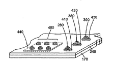
除了对该等焊接凸块280、360等提供经改善的结构性保护以外,本说明书中所揭露的绝缘层240放置使得该凸块下方金属化层230能够作为电性绕线结构。通过参照第19图可了解示范实施例,第19图放置有绝缘层240与数个面朝上凸块的半导体装置170的一部分的示意图。其中一个凸块如同第8图至第12图中标示为280。另外两个凸块分别标示为380与390。六个凸块的群组集中标示为400。可形成该等凸块280、380及390并设置有离散的凸块下方导体结构(under bumpconductor structure)或金属层410、420及430,该等凸块下方导体结构或金属层利用本说明书中所揭露的技术而结构性隔离。该等金属层410、420及430由该绝缘层240所覆盖,因此显示为虚线图案。然而,可利用本说明书中所揭露的技术形成该凸块群组400,但是具有共同的凸块下方导体结构或金属层440,该凸块下方导体结构或金属层由该绝缘层240所覆盖,因此亦显示为虚线图案。因此,该绝缘层240在形成该等凸块400之前形成有多个开口,以显露出该金属层440的多个部分。如此一来,该金属层440可作为用在该凸块群组400的绕线结构。有利的地方在于,数个凸块暂时或长久地作为一种类型的输入/输出,如电源或接地。因为该绝缘层240位在该凸块群组400与该金属化层440之间,故可将经选定的凸块联系在一起而不会有在回焊期间焊接将侧向地渗出并产生非所欲的短路的风险。当然,凸块的数量和群组分类与该共同凸块下方金属化层440的形状具有相当大的变化性。
熟习本领域者将体认到,本说明书中所揭露的示范程序可同时实施在布设在晶圆中的多个晶粒上。接着,可实施切单(singulation)。在切单后,可选择性地处理个别晶粒。
可以多种方式接置该半导体装置170。第20图描绘了几个示范接置可能性的爆炸示意图。该半导体装置170经描绘成具有面朝上的焊接凸块280。该半导体装置170可如箭头450所指出般经翻转并且覆晶接置在基板460上。该基板460可为封装件基板、印刷电路板或其他类型基板。倘若组构如封装件基板,该机板460可为接脚栅阵列(pin gridarray)、球栅阵列、平面栅阵列(land grid array)、表面接置或其他类型组构。该基板460可接置至另一基板470。该基板470可为印刷电路板或其他类型基板。举例而言,该基板470可为用在计算机系统的主机板。该半导体装置170可包含在更大的系统(如虚线盒480所表示的运算装置)中。该运算装置480可包含例如数位电视、手持式行动装置、个人计算机、伺服器、记忆体装置、如绘图卡的添加电路板、或其他任何采用半导体的运算装置。
上述所讨论的第19图描绘将UBM结构用在电性绕线(electricalrouting)的范例。第23图至第30图描绘了数个使用UBM布设的复杂绕线的范例。在参照这些图式进行讨论之前,简要地回顾习知用在使用焊接结构作为输入/输出的半导体芯片的电性绕线设计将有所助益。第21图示范的习知半导体芯片500放置成底部侧(bottom side)朝上而显示出多个导体球的示意图。该等导体球其中两个标示为510与515。在接置至印刷电路板(未显示)的期间,该半导体芯片500经翻转,使得该等导体球510、515等面朝下,并且与该印刷电路板上对应的焊接结构形成冶金连接(metallurgical connection)。该等焊接球510、515等互连至该芯片500的本体中各种电路结构(未显示在第21图)。然而,该等焊接球510与515间一些示范互连结构与该芯片500中的电路结构放大显示在第22图中。
請参照第22图,第22图是第21图所描绘的两个焊接球510与515以及自该等焊接球510与515向下导引至该芯片500中两个示范习知电子装置520与525的典型互连结构的示意图。应了解到,存在该等焊接球510和515与该等电子装置520和525间的区域527中的多个绝缘层并未显示出来,使得该等电子装置520和525与该等焊接球510和515间的电性互连的细节清楚可见。该等电子装置520与525是描绘成场效电晶体,其具有个别柵極(gate)530与535。两个金属化层540与545及重新分配层(RDL)550插入该等焊接球510和515与该等电子装置520和525间。该金属化层540由多条金属线所构成,所显示的其中两条金属线标示为555与560。该金属化层545类似地由多条金属线所构成,所显示的其中两条金属线标示为565与567,而该重新分配层550由多条金属线所构成,所显示的其中两条金属线标示为570与575。该金属结构555经由接点580(contact)而电性连接至该装置520的柵極530。该等金属结构555与565通过盲孔585(via)电性连接,而该RDL结构570经由盲孔590电性连接至该金属层结构565。接点595与两个盲孔600和605设置成用以将该RDL结构575电性连结至该装置525的柵極535。该等焊接球510与515经由个别的UBM球或焊接垫片610与615、以及导体延伸617与619(conductor extension)而电性连接至个别的RDL结构570与575。
该RDL 550设计成用以在第21图所示焊接球510与515及其他焊接球的绕线与布局(layout)中提供额外的弹性。因为制造该等焊接球典型上在热回焊期间具有一些风险(初始未对准(initial misalignment)或溢出(spill over)与随后发生的短路),故为了减轻此类交叉污染(crosscontamination)与短路的机会,该重新分配层550的RDL结构570与575必须维持某种最小间距X1。
现通过参照第23图与第24图可理解半导体芯片或装置纳入有用在复杂绕线的UBM层的示范实施例。第23图是半导体芯片或装置620显示为底部侧朝上以显现出多个焊接结构的示范实施例的示意图,其中两个焊接结构标示为623与625。该芯片620可包含大量的(数百或数千个)焊接结构。然而,为了简化图式,第23图中仅仅显示几个此类焊接结构。注意到,标示为630的位置没有焊接结构。此省略的重要性将参照第24图进行详述。该半导体装置620可为任何使用在电子设备中的大量不同类型的电路装置,如微处理器、图形处理器、特殊应用积体电路、记忆体装置或类似装置,且可为单一或者多个核心。
請参照第24图,第24图以示意并且放大的形式描绘第23图所描绘的焊接结构625与该半导体芯片620的位置630两者。该半导体芯片620中也许数百万个电路装置的其中两个描绘在第24图中,并且分别标示为635与640。该等电路装置635与640描绘成场效电晶体,然而,两者可为任何使用在积体电路中的大量不同类型的电路装置。该等电晶体635与640具有个别柵極645与650,该等柵極645与650经由接点670与675而连接至金属化层665的个别金属线655与660。第二金属化层680由经由盲孔695与700连接至该金属层665的金属线685与690所构成。尽管仅描绘两个金属化层665与680,但取决于半导体芯片620的复杂度,可以有更多的金属化层。
由多个RDL结构(所显示的其中两个标示为710与715)所构成的重新分配层705设置成用以形成该等焊接球623(如第23图所示)与625及该等衬底电路装置间的电性绕线。该重新分配层705较有利的情况是由许多导体线所组成,有利于制造有相对较大尺寸及/或提供优先的低欧姆损失的其他性质。该RDL结构710经由盲孔717连接至该金属线685,而该RDL结构715经由盲孔719连接至该金属线690。由此看来,第24图所描绘的结构几乎与第22图所描绘的习知焊接球和绕线结构完全相同。然而,在此说明实施例中,导体或UBM结构720(其可为部分更加扩张的UBM层)插入该焊接球625与该RDL结构710和715之间并且电性连接至该焊接球625与该RDL结构710和715。该UBM结构720包含通过跨越构件727(cross-member)而联系在一起的多个垫片或部位723与725,并且通过两个延伸构件729与731(extensionmember)分别连接至该等RDL结构710与715。如此一来,可消除通常必须置在该垫片725上的位置630以对该RDL结构715提供输入/输出的焊接球735,该等RDL结构710与715可挤得更为接近而具有最小间距X2,该最小间距X2可小于第22图所描绘的习知结构的最小间距X1。该UBM结构720的垫片部位723与725共同电性连接至该等电晶体635与640的柵極645与650。因此,该UBM结构720应该用以共同地联系用在相同类型电性信号(例如:电源、接地或各种情况的信号)的球/凸块部位。尽管该UBM结构720描绘成简单的马蹄形装置,但应理解到,该UBM结构720可采用很多种不同组构且可伴随大量类似的UBM结构,该等类似的UBM结构以各种方式联系描绘在第23图中该半导体芯片620上的各种导体凸块。应了解到,可利用本说明书其他部分所揭露的技术与材料来制造该UBM结构720。
請参照第25图,第25图是第23图所描绘的半导体芯片620的小部分以及几个分解自该芯片620的焊接球740、745、750、755及760的示意图。该半导体芯片620的大量外部电路结构的其中几个由虚线盒A、B、C、D、E、F、G及H示意地表示。该等电路结构A、B、C、D、E、F、G及H可为例如电源轨(rail)、接地轨、电容器、较大的积体电路功能性方块、记忆体装置、处理器核心或实质上使用在半导体芯片中的任何电路。该等电路结构A、B、C、D、E、F、G及H经由个别的互连而电性连接至个别的RDL结构765、770、775、780、785、790、795及800,该等互连由单端箭头线805、810、815、820、825、830、835及840示意地表示。该等互连805、810、815、820、825、830、835及840可由一层或多层金属化或其他导体材料层所构成,如第24图所描绘的多重金属化层665与680。导体垫片845、850、855及860分别连接至该等RDL结构770、780、790及800。该等焊接球745、750、755及760接置至该等导体垫片845、850、855及860。
导体垫片865、870、875及880分别连接至该等RDL结构765、775、785及795。该等导体垫片865、870、875及880电性联系在一起并且制造成部分UBM结构885,而该UBM结构885经成型为类似格栅的结构。该UBM结构885可通过个别的延伸而连接至该等衬底RDL结构765、775、785及795,所显示的其中一者接近该垫片部位865并且标示为890。确实,该等垫片845、850、855及860可利用未显示的类似延伸。该焊接球740在该垫片865连接至该UBM结构885。如此一来,经由该焊接球740的电性输入/输出为所有焊接垫片865、870、875及880以及该等衬底电路结构A、C、D及F所设置。用在该UBM结构885的类似格栅结构具有布局相对较小的优点,可轻易地进行微影图案化并利用广为熟知的技术来形成。此外,此类结构提供了相对高效率的电流传送且因此提供相对较小的欧姆损失。由于所有导体垫片865、870、875及880皆共同连接且为部分该UBM结构885,该些焊接垫片典型上将用于特殊类型的电性输入/输出,如接地、电源或信号。其他垫片845、850、855及860视情况而定可连接成电源、接地或信号输入/输出。当然,为了简化制造,所有垫片845、850、855、860、865、870、875及880皆可在相同层次上制造。
该UBM结构885能够排除通常必须放置在垫片870、875及880的焊接球。因此,剩余的焊接球740、745、750、755及760的总体布设可相应地更为紧密。
利用所揭露的UBM结构对于潜在绕线具有相当大的弹性。請参照第26图,第26图是小部分该芯片620的平面图。在此,为了简化图式,描绘有三个格栅类型的UBM结构915、920及925,其可为UBM层延伸之部分,其中与周围没有描绘任何绝缘材料。首先,参照有关于该UBM结构915的位置,导体垫片930(显示为虚线图案)、935、940及945显示成连接至个别RDL层结构950、955、960及965。该等重新分配层结构950、955、960及965位在该等垫片930、935、940及945下,并且电性连接至该半导体芯片620内部的其他互连或电路结构。该等导体垫片930、935、940及945联系至该芯片620的电源路径,并因此为了电源输入/输出而标注为”P”。然而,包含该UBM结构915使得所有垫片930、935、940及945的电源输入/输出透过位置接近该导体垫片930的单一焊接球970而绕线上来。数个其他导体或焊接垫片975、980、985及990可聚集在该UBM结构915中与周围,联系至该芯片620的信号路径,并因此为了电源输入/输出信号而标注为例如”S”。就这点而言,该等垫片975、980、985及990可电性联系至个别的RDL结构995、1000、1005及1010,并且设置有个别的焊接球1015、1020、1025及1030。
以类似的方式,该UBM结构920可组构成用以将多个接地路径位置(标注为”G”)绕线至焊接垫片1035(显示为虚线图案)与对应的焊接球1040,而该UBM结构925可组构成用以将多个电源输入/输出部位绕线至导体垫片1045(显示为虚线图案)与焊接凸块1050。当然,该等UBM结构915、920及925可同时结合多个导体垫片1055、1060、1065、1070及1075,各该导体垫片皆设置有个别的焊接凸块1080、1085、1090、1095及1100,其中该等导体垫片1055、1060、1065、1070及1075欧姆连接至个别的RDL结构1105、1110、1115、1120及1125。此布设可能是适当的,举例而言,该等导体垫片1055与1060经选定用在接地输入/输出,该导体垫片1065经选定用在电源输入/输出,而该等导体垫片1070与1075经选定用在信号输入/输出。重点是传统的焊接凸块至RDL互连两者皆可与该UBM绕线结构共同使用,以达到所欲的布局图案。
請参照第27图,第27图是半导体芯片620的另一部分的平面图。在此部分中,可看到UBM结构1130与一组电性连接至该UBM结构1130并且形成部分该UBM结构1130的导体垫片1135(显示为虚线图案)、1140、1145及1150。为了简化图式,描绘该UBM结构1130与该等垫片1135、1140、1145及1150,而未描绘任何周围的与覆盖的绝缘材料。该等导体垫片1135、1140、1145及1150可联系至个别的RDL结构1155、1160、1165及1170。该等导体垫片1135、1140、1145及1150可经由单一凸块1173而经选定用在电源输入/输出,该单一凸块1173连接至如图所示接近该垫片1135的UBM 1130。此外,可设置其他垫片1175、1180、1185及1190,并且经选定用在信号输入/输出。焊接凸块1195、1200、1205及1210可分别设置在该等垫片1175、1180、1185及1190上。注意到,一部分该凸块1210经切去,以显现出该导体垫片1190的额外细节。在本说明实施例中,相对在本说明书其他部分所揭露的圆形或八角形结构,该焊接垫片1190可组构成矩形结构。矩形结构具有能够更紧密包装导体垫片与其相关的RDL结构的优点。确实,电性连接至该UBM结构1130的导体垫片1140与1150是描绘成矩形结构。
第28图显示半导体芯片1215的另一说明实施例的平面图。为了简化图式,仅描绘小部分的半导体芯片1215,而未描绘任何周围的与覆盖的绝缘材料。显示示范UBM结构1220位在数个RDL结构1225、1230、1235、1240及1245上方。该UBM结构1220可设置有具数个引脚结构的丛集1250、1255及1260。该丛集1250可由多个引脚1265、1270、1275、1280、1285、1290、1295及1300所构成,该等引脚通过个别的长柄(spoke)1310、1315、1320、1325、1330、1335、1340及1345而连接至中央集线部(central hub)。如长柄1310、1320、1330及1340的情况下,该等长柄的个别引脚无须中断。该引脚1265电性连接至该衬底RDL结构1225,该等引脚1270与1300连接至该衬底RDL结构1230,该等引脚1280与1290连接至该衬底RDL结构1235,而该引脚1285连接至该衬底RDL结构1240。该集线部1305可设置有经选定用在接地输入/输出的焊接凸块1350。
该丛集1255可包含集线部1355与多个自该丛集1255延伸离开但通过个别长柄1380、1385、1390及1395连接至该丛集1255的引脚1360、1365、1370及1375。该等引脚1360与1365连接至该衬底RDL结构1245,而该等引脚1370与1375连接至该衬底RDL结构1235。该丛集1255可在如图所示的引脚1295或所欲的其他点联系至该丛集1250。焊接球1397可连接至该集线部1355。
最终,该丛集1260可由集线部1400、长柄1405、1410、1415、1420及1423与分别连接至该等长柄1405、1410、1415、1420的引脚1425、1430、1435及1440所构成。该等引脚1425与1430可连接至该衬底RDL结构1245,而该等引脚1435与1440可连接至该衬底RDL结构1235。类似该等丛集1250与1255,该丛集1260可设置有经选定用在接地输入/输出的焊接凸块1450。该电源凸块1460与1465连接至衬底RDL结构1470与1475。在转向参照第29图之前,重要的是注意位置。
請参照第29图,第29图是第28图以29-29为截线的剖面图。在决定第29图的细节前,应注意到:(1)截线29-29通过该引脚1430、该集线部1400、焊接球1450、该引脚1440组合及该焊接球1465;以及(2)第29图确实描绘出该半导体芯片1215并未描绘在第28图的一些细节,使得可观察得到各种导体结构与UBM结构的其他细节。因此,举例而言,该两个焊接凸块1450与1465经由聚酰亚胺或其他聚合物材料薄膜1485而侧向分隔并且侧向电性绝缘。再者,应记得,该薄膜1485并未描绘在第28图,使得所描述的其他结构不致混淆。尤其,该焊接球1465下有UBM结构1490,该UBM结构1490通过间隙1493(gap)而侧向地与该UBM丛集1260分隔。该间隙1493填充有部分绝缘材料层1495的绝缘材料。该绝缘材料层1495可组构成类似上述保护层同时结合本说明书其他部分所揭露的其他实施例。如同本说明书其他部分所提及,欧姆接点形成在该焊接球1450与该衬底UBM结构(在此情况下,為该集线部1400)之间。该集线部1400经由引脚或延伸1503而与衬底RDL结构1500(未显示在第28图)发生欧姆接触。该等引脚1430与1440与该等衬底RDL结构1245与1235发生欧姆接触。该等RDL结构1245、1500及1235电性连接至由虚线盒I、J及K所表示的电路结构,该等电路结构位在该半导体芯片1215的更深处。该等电路结构I、J及K一般而言可为上述类型同时结合第25图中该等电路结构A、B、C、D等。该焊接凸块1465与衬底UBM结构1490发生欧姆接触,该衬底UBM结构1490经由延伸或引脚1507(未显示在第28图)而与RDL结构1505发生欧姆接触。该RDL结构1505连接至由该虚线盒L所表示的衬底电路,该衬底电路可组构成上述电路结构I、J及K。
丛集结构可用在电源、接地或信号。无论是用在电源、接地或信号输入/输出,使用丛集布设的优点是紧密的包装与更大的布局弹性。熟习本领域者将体认到,对给定的丛集而言,引脚与长柄的数量是可变动的。此外,丛集布设可利用本说明书所揭露的其他类型UBM结构。
第30图是半导体芯片620自印刷电路板1510向上剥开的示意图,该印刷电路板1510可为半导体芯片封装件基板或其他类型的印刷电路板。当组装时,该半导体芯片620覆晶接置在该封装件基板1510的凸块阵列1515上。该凸块阵列1515包含多个面朝上的焊接凸块,其中一者标示为1520,设计成用以接合该半导体芯片620的焊接凸块623、625等。该基板1510包含一些类型的互连结构,以形成与一些连接至该基板1510的其他电子装置的输入/输出。在本说明实施例中,由多个接脚(其中一者标示为1525)所构成的接脚栅阵列突出自该基板1510。然而,可使用球栅阵列、平面栅阵列或其他类型的互连。给定的接脚(如接脚1525)与给定的凸块位置(如凸块位置1520)间经由电性互连结构而在该基板1510上形成有电性路径,该电性路径示意地由虚线1530表示。该互连结构1530可由一条或多条导体线所构成,该等导体线可能是或可能不是在该基板1510中一个或多个不同层次的互连上。
为了各种理由,围绕在该凸块阵列1515的周围1535的凸块位置倾向用在信号输入/输出,而该凸块阵列1515的核心垫片位置1540(corepad location)倾向用在电源与接地输入/输出。此传统设计方法满足许多设计情况。然而,有某些设计情况,其中所谓的深凸块(亦即,如该半导体芯片620上位置相对接近该芯片620的边缘1550的凸块623)需要电源或接地输入/输出。由于该阵列1515的周围凸块位置1535倾向用在信号输入/输出,故为了将电源或接地自给定的接脚1525绕线至该阵列1515上位在周围的垫片部位,必须在该基板1510中制作一些种类的埋植互连布设(buried interconnect arrangement)。倘若该基板轨迹绕线(substrate trace routing)必须经显着的修改,则此解决方案可能存在有成本损失与可能的效能问题。然而,如本说明书所揭露的UBM绕线可用以将电源或接地输入/输出绕线至此类深凸块623。就这点而言,UBM绕线结构1555电性连接至该芯片620的深凸块623与其中一个位在中央的凸块1560。由于将有绝缘材料配置在该等凸块623与1560及该衬底UBM结构1555间,故该UBM结构1555以虚线图案显示。该UBM结构1555可组构成本说明书所揭露的任何一个实施例所描述者。
本说明书所揭露的任何示范实施例皆可体现为配置在计算机可读取媒体(如半导体、磁盘、光盘或其他存储媒体或如同计算机资料信号)中的指令。该指令或软件能够合成及/或模拟本说明书所揭露的电路结构。在示范实施例中,电子设计自动化程序(如Cadence APD或类似程序)可用以合成所揭露的电路结构。所产生的程序码可用以制造所揭露的电路结构。在另一示范实施例中,模拟程序(如高频SPICE模拟器或类似程序)可用以模拟所揭露的电路结构的电性行为。
尽管本发明可容许各种修改与替代形式,但是特定实施例已通过附加图式的范例显示并且已详述在本说明书中。然而,应理解到,本发明并非意图限定在所揭露的特定形式。相反地,本发明意图涵盖落在由附加申请专利范围所定义的本发明精神与范畴内的所有修改、等效与替代形式。
Claims (27)
1.一种制造方法,包括:
在半导体芯片上形成导体结构,该导体结构具有电性连接至第一重新分配层结构的第一部位以及电性连接至第二重新分配层结构的第二部位;以及
在该导体结构上形成焊接结构。
2.如权利要求1所述的方法,包括在接近该第一部位的该导体结构上形成该焊接结构。
3.如权利要求1所述的方法,包括在接近该第二部位的该导体结构上不形成焊接结构。
4.如权利要求1所述的方法,其中,该形成该导体结构包括形成导体格栅,该导体格栅具有电性耦接至该第一重新分配层结构的该第一部位以及电性耦接至该第二重新分配层结构的该第二部位。
5.如权利要求1所述的方法,其中,该形成该导体结构包括形成丛集,该丛集具有集线部以及耦接至该集线部的至少该第一和第二部位,该第一部位连接至该第一重新分配层结构而该第二部位连接至该第二重新分配层结构。
6.如上述任一权利要求所述的方法,包括将该半导体芯片耦接至基板并且将该基板接置于运算装置中。
7.如上述任一权利要求所述的方法,其中,该方法通过执行计算机可读取媒体中所存储的指令而实施。
8.一种制造方法,包括:
在半导体芯片上形成第一导体结构,该第一导体结构具有电性连接至第一重新分配层结构的第一部位以及电性连接至第二重新分配层结构的第二部位;
在该半导体芯片上形成第二导体结构,该第二导体结构具有电性连接至第三重新分配层结构的第三部位以及电性连接至第四重新分配层结构的第四部位;以及
在该第一导体结构上形成第一焊接结构并且在该第二导体结构上形成第二焊接结构。
9.如权利要求8所述的方法,包括将该第一焊接结构电性连接至该半导体芯片的接地路径以及将该第二焊接结构电性连接至该半导体芯片的电源路径。
10.如权利要求8所述的方法,其中,该形成该第一导体结构包括形成导体格栅,该导体格栅具有电性耦接至该第一重新分配层结构的该第一部位以及电性耦接至该第二重新分配层结构的该第二部位。
11.如权利要求8至10中任何一项所述的方法,其中,该形成该第二导体结构包括形成丛集,该丛集具有集线部以及耦接至该集线部的至少该第三和第四部位,该第三部位连接至该第三重新分配层结构而该第四部位连接至该第四重新分配层结构。
12.如权利要求8所述的方法,包括在接近该第一部位的该第一导体结构上形成该第一焊接结构。
13.如权利要求8所述的方法,包括在接近该第二部位的该第一导体结构上不形成焊接结构。
14.如权利要求8至13中任何一项所述的方法,包括将该半导体芯片耦接至基板并且将该基板接置于运算装置中。
15.如权利要求8至14中任何一项所述的方法,其中,该方法通过执行计算机可读取媒体中所存储的指令而实施。
16.一种制造方法,包括:
在半导体芯片上形成导体结构,该导体结构具有电性连接至重新分配层结构的多个部位;以及
在接近该多个部位的其中一个的该导体结构上形成至少一个焊接结构。
17.如权利要求16所述的方法,包括将该至少一个焊接结构电性连接至该半导体芯片的电源路径。
18.如权利要求16所述的方法,包括将该至少一个焊接结构电性连接至该半导体芯片的接地路径。
19.如权利要求16所述的方法,包括在接近其他该多个导体垫片的该导体结构上不形成焊接结构。
20.一种设备,包括:
半导体芯片,其具有至少两个重新分配层结构;
导体结构,其在该半导体芯片上,该导体结构具有电性连接至该至少两个重新分配层结构的第一个的第一部位以及电性连接至该至少两个重新分配层结构的第二个的第二部位;以及
焊接结构,其在该导体结构上。
21.如权利要求20所述的设备,其中,该至少两个重新分配层结构包括部分相同类型的电性路径。
22.如权利要求20所述的设备,其中,该导体结构包括导体格栅,该导体格栅具有耦接至该至少两个重新分配层结构的第一个的该第一部位以及耦接至该至少两个重新分配层结构的第二个的该第二部位。
23.如权利要求20所述的设备,其中,该导体结构包括丛集,该丛集具有集线部以及耦接至该集线部的该第一和第二部位。
24.如权利要求20所述的设备,其中,该焊接结构定位于接近该第一部位的该导体结构上。
25.如权利要求20所述的设备,其中,在接近该第二部位的该第一导体结构上没有焊接结构。
26.如权利要求20至25中任何一项所述的设备,包括耦接至该半导体芯片的基板。
27.如权利要求26所述的设备,包括耦接至该基板的运算装置。
Applications Claiming Priority (3)
| Application Number | Priority Date | Filing Date | Title |
|---|---|---|---|
| US11/949,951 | 2007-12-04 | ||
| US11/949,951 US20090032941A1 (en) | 2007-08-01 | 2007-12-04 | Under Bump Routing Layer Method and Apparatus |
| PCT/IB2008/003343 WO2009071982A2 (en) | 2007-12-04 | 2008-12-04 | Under bump routing layer method and apparatus |
Publications (1)
| Publication Number | Publication Date |
|---|---|
| CN101952962A true CN101952962A (zh) | 2011-01-19 |
Family
ID=40592064
Family Applications (1)
| Application Number | Title | Priority Date | Filing Date |
|---|---|---|---|
| CN2008801260899A Pending CN101952962A (zh) | 2007-12-04 | 2008-12-04 | 凸块下方绕线层方法及设备 |
Country Status (6)
| Country | Link |
|---|---|
| US (1) | US20090032941A1 (zh) |
| EP (1) | EP2229694B1 (zh) |
| JP (2) | JP5567489B2 (zh) |
| KR (1) | KR20100102635A (zh) |
| CN (1) | CN101952962A (zh) |
| WO (1) | WO2009071982A2 (zh) |
Cited By (1)
| Publication number | Priority date | Publication date | Assignee | Title |
|---|---|---|---|---|
| CN103887248A (zh) * | 2012-12-21 | 2014-06-25 | 比亚迪股份有限公司 | 一种igbt结构及其制备方法 |
Families Citing this family (14)
| Publication number | Priority date | Publication date | Assignee | Title |
|---|---|---|---|---|
| US7790501B2 (en) * | 2008-07-02 | 2010-09-07 | Ati Technologies Ulc | Semiconductor chip passivation structures and methods of making the same |
| US8278748B2 (en) * | 2010-02-17 | 2012-10-02 | Maxim Integrated Products, Inc. | Wafer-level packaged device having self-assembled resilient leads |
| TWI541964B (zh) * | 2010-11-23 | 2016-07-11 | 矽品精密工業股份有限公司 | 半導體基板之製法 |
| US20120175772A1 (en) * | 2011-01-07 | 2012-07-12 | Leung Andrew K | Alternative surface finishes for flip-chip ball grid arrays |
| US8647974B2 (en) | 2011-03-25 | 2014-02-11 | Ati Technologies Ulc | Method of fabricating a semiconductor chip with supportive terminal pad |
| US8564030B2 (en) | 2011-06-10 | 2013-10-22 | Advanced Micro Devices | Self-aligned trench contact and local interconnect with replacement gate process |
| US8716124B2 (en) | 2011-11-14 | 2014-05-06 | Advanced Micro Devices | Trench silicide and gate open with local interconnect with replacement gate process |
| US9257276B2 (en) * | 2011-12-31 | 2016-02-09 | Intel Corporation | Organic thin film passivation of metal interconnections |
| WO2013101243A1 (en) | 2011-12-31 | 2013-07-04 | Intel Corporation | High density package interconnects |
| US20140159130A1 (en) * | 2012-11-30 | 2014-06-12 | Enpirion, Inc. | Apparatus including a semiconductor device coupled to a decoupling device |
| GB2520952A (en) * | 2013-12-04 | 2015-06-10 | Ibm | Flip-chip electronic device with carrier having heat dissipation elements free of solder mask |
| JP6771308B2 (ja) * | 2016-05-02 | 2020-10-21 | 三菱電機株式会社 | 回路基板および半導体集積回路の実装構造 |
| WO2019116482A1 (ja) * | 2017-12-14 | 2019-06-20 | 三菱電機株式会社 | 半導体装置 |
| CN114695224A (zh) * | 2020-12-29 | 2022-07-01 | 联华电子股份有限公司 | 芯片键合对准结构与键合芯片结构及其制作方法 |
Family Cites Families (47)
| Publication number | Priority date | Publication date | Assignee | Title |
|---|---|---|---|---|
| US3593319A (en) * | 1968-12-23 | 1971-07-13 | Gen Electric | Card-changeable capacitor read-only memory |
| US4249196A (en) * | 1978-08-21 | 1981-02-03 | Burroughs Corporation | Integrated circuit module with integral capacitor |
| JPS56101732A (en) * | 1980-01-18 | 1981-08-14 | Matsushita Electric Ind Co Ltd | Metallized film condenser |
| US4409608A (en) * | 1981-04-28 | 1983-10-11 | The United States Of America As Represented By The Secretary Of The Navy | Recessed interdigitated integrated capacitor |
| GB2115223B (en) * | 1982-02-18 | 1985-07-10 | Standard Telephones Cables Ltd | Multilayer ceramic dielectric capacitors |
| US4901128A (en) * | 1982-11-04 | 1990-02-13 | Hitachi, Ltd. | Semiconductor memory |
| KR900001394B1 (en) * | 1985-04-05 | 1990-03-09 | Fujitsu Ltd | Super high frequency intergrated circuit device |
| US4685197A (en) * | 1986-01-07 | 1987-08-11 | Texas Instruments Incorporated | Fabricating a stacked capacitor |
| DE3783652T2 (de) * | 1986-05-16 | 1993-06-03 | Showa Denko Kk | Festelektrolytkondensator. |
| JPS6370550A (ja) * | 1986-09-12 | 1988-03-30 | Nec Corp | 半導体集積回路装置 |
| JPH01209746A (ja) * | 1988-02-17 | 1989-08-23 | Nec Corp | 半導体装置 |
| US4866567A (en) * | 1989-01-06 | 1989-09-12 | Ncr Corporation | High frequency integrated circuit channel capacitor |
| US4914546A (en) * | 1989-02-03 | 1990-04-03 | Micrel Incorporated | Stacked multi-polysilicon layer capacitor |
| US5053916A (en) * | 1989-03-13 | 1991-10-01 | U.S. Philips Corporation | Surface-mounted multilayer capacitor and printed circuit board having such a multilayer capacitor |
| US5089878A (en) * | 1989-06-09 | 1992-02-18 | Lee Jaesup N | Low impedance packaging |
| US5081559A (en) * | 1991-02-28 | 1992-01-14 | Micron Technology, Inc. | Enclosed ferroelectric stacked capacitor |
| US5189594A (en) * | 1991-09-20 | 1993-02-23 | Rohm Co., Ltd. | Capacitor in a semiconductor integrated circuit and non-volatile memory using same |
| US5155658A (en) * | 1992-03-05 | 1992-10-13 | Bell Communications Research, Inc. | Crystallographically aligned ferroelectric films usable in memories and method of crystallographically aligning perovskite films |
| US5208725A (en) * | 1992-08-19 | 1993-05-04 | Akcasu Osman E | High capacitance structure in a semiconductor device |
| JP3057130B2 (ja) * | 1993-02-18 | 2000-06-26 | 三菱電機株式会社 | 樹脂封止型半導体パッケージおよびその製造方法 |
| JP3160198B2 (ja) * | 1995-02-08 | 2001-04-23 | インターナショナル・ビジネス・マシーンズ・コーポレ−ション | デカップリング・コンデンサが形成された半導体基板及びこれの製造方法 |
| US5874782A (en) * | 1995-08-24 | 1999-02-23 | International Business Machines Corporation | Wafer with elevated contact structures |
| JP3147162B2 (ja) * | 1998-07-13 | 2001-03-19 | 日本電気株式会社 | フリップチップ集積回路のバンプ配置方法、およびフリップチップ集積回路 |
| JP3530761B2 (ja) * | 1999-01-18 | 2004-05-24 | 新光電気工業株式会社 | 半導体装置 |
| WO2000044043A1 (fr) * | 1999-01-22 | 2000-07-27 | Hitachi, Ltd. | Dispositif a semi-conducteurs et son procede de fabrication |
| JP4004196B2 (ja) * | 1999-11-16 | 2007-11-07 | イビデン株式会社 | 半導体チップ |
| JP2001168125A (ja) * | 1999-12-03 | 2001-06-22 | Nec Corp | 半導体装置 |
| US6387795B1 (en) * | 2001-03-22 | 2002-05-14 | Apack Technologies Inc. | Wafer-level packaging |
| US7215022B2 (en) * | 2001-06-21 | 2007-05-08 | Ati Technologies Inc. | Multi-die module |
| WO2003012863A1 (en) * | 2001-07-31 | 2003-02-13 | Renesas Technology Corp. | Semiconductor device and its manufacturing method |
| US6979896B2 (en) * | 2001-10-30 | 2005-12-27 | Intel Corporation | Power gridding scheme |
| JP3768433B2 (ja) * | 2001-11-19 | 2006-04-19 | 株式会社ルネサステクノロジ | 半導体装置の設計方法 |
| DE10159466A1 (de) * | 2001-12-04 | 2003-06-12 | Koninkl Philips Electronics Nv | Anordnung mit Kondensator |
| JP2004079801A (ja) * | 2002-08-19 | 2004-03-11 | Fujitsu Ltd | コンデンサ装置及びその製造方法 |
| US7112884B2 (en) * | 2002-08-23 | 2006-09-26 | Ati Technologies, Inc. | Integrated circuit having memory disposed thereon and method of making thereof |
| US6861749B2 (en) * | 2002-09-20 | 2005-03-01 | Himax Technologies, Inc. | Semiconductor device with bump electrodes |
| US7161793B2 (en) * | 2002-11-14 | 2007-01-09 | Fujitsu Limited | Layer capacitor element and production process as well as electronic device |
| JP4571781B2 (ja) * | 2003-03-26 | 2010-10-27 | ルネサスエレクトロニクス株式会社 | 半導体装置およびその製造方法 |
| US7180195B2 (en) * | 2003-12-17 | 2007-02-20 | Intel Corporation | Method and apparatus for improved power routing |
| JP4904670B2 (ja) * | 2004-06-02 | 2012-03-28 | 富士通セミコンダクター株式会社 | 半導体装置 |
| TWI299248B (en) * | 2004-09-09 | 2008-07-21 | Phoenix Prec Technology Corp | Method for fabricating conductive bumps of a circuit board |
| JP4449824B2 (ja) * | 2005-06-01 | 2010-04-14 | カシオ計算機株式会社 | 半導体装置およびその実装構造 |
| US7473999B2 (en) * | 2005-09-23 | 2009-01-06 | Megica Corporation | Semiconductor chip and process for forming the same |
| JP4595823B2 (ja) * | 2006-01-24 | 2010-12-08 | 株式会社デンソー | ボールグリッドアレイ |
| US20070176292A1 (en) * | 2006-01-27 | 2007-08-02 | Taiwan Semiconductor Manufacturing Co., Ltd. | Bonding pad structure |
| JP5157191B2 (ja) * | 2006-03-01 | 2013-03-06 | 日立化成株式会社 | 半導体装置 |
| JP2006203261A (ja) * | 2006-04-26 | 2006-08-03 | Renesas Technology Corp | 半導体装置 |
-
2007
- 2007-12-04 US US11/949,951 patent/US20090032941A1/en not_active Abandoned
-
2008
- 2008-12-04 CN CN2008801260899A patent/CN101952962A/zh active Pending
- 2008-12-04 WO PCT/IB2008/003343 patent/WO2009071982A2/en active Application Filing
- 2008-12-04 JP JP2010536543A patent/JP5567489B2/ja not_active Expired - Fee Related
- 2008-12-04 KR KR1020107014910A patent/KR20100102635A/ko not_active Application Discontinuation
- 2008-12-04 EP EP08855955.4A patent/EP2229694B1/en active Active
-
2013
- 2013-02-19 JP JP2013030065A patent/JP5654067B2/ja not_active Expired - Fee Related
Cited By (1)
| Publication number | Priority date | Publication date | Assignee | Title |
|---|---|---|---|---|
| CN103887248A (zh) * | 2012-12-21 | 2014-06-25 | 比亚迪股份有限公司 | 一种igbt结构及其制备方法 |
Also Published As
| Publication number | Publication date |
|---|---|
| JP5654067B2 (ja) | 2015-01-14 |
| JP2013093630A (ja) | 2013-05-16 |
| WO2009071982A2 (en) | 2009-06-11 |
| EP2229694A2 (en) | 2010-09-22 |
| EP2229694B1 (en) | 2017-01-25 |
| JP2011505705A (ja) | 2011-02-24 |
| WO2009071982A3 (en) | 2009-07-23 |
| KR20100102635A (ko) | 2010-09-24 |
| JP5567489B2 (ja) | 2014-08-06 |
| US20090032941A1 (en) | 2009-02-05 |
Similar Documents
| Publication | Publication Date | Title |
|---|---|---|
| CN101952962A (zh) | 凸块下方绕线层方法及设备 | |
| US7670939B2 (en) | Semiconductor chip bump connection apparatus and method | |
| JP4660643B2 (ja) | プリ半田構造を形成するための半導体パッケージ基板及びプリ半田構造が形成された半導体パッケージ基板、並びにこれらの製法 | |
| TWI254995B (en) | Presolder structure formed on semiconductor package substrate and method for fabricating the same | |
| TWI261329B (en) | Conductive bump structure of circuit board and method for fabricating the same | |
| TWI517273B (zh) | 具有支撐終端墊的半導體晶片 | |
| CN103325760B (zh) | 形成于半导体基板上的导电凸块及其制法 | |
| US10475760B2 (en) | Semiconductor device | |
| US20060252248A1 (en) | Method for fabricating electrically connecting structure of circuit board | |
| TW201208022A (en) | Flip chip package assembly and process for making same | |
| KR20110124993A (ko) | 반도체 칩 및 이를 포함하는 반도체 패키지 및 반도체 칩의 제조 방법 | |
| KR20130096990A (ko) | 반도체 장치 | |
| WO2009016495A1 (en) | Semiconductor device having a bump electrode and method for its manufacture | |
| CN104584206B (zh) | 用于互连附着的迹线沾焊料技术 | |
| CN101360388B (zh) | 电路板的电性连接端结构及其制法 | |
| CN105633053A (zh) | 基板结构及其制法 | |
| CN101587842A (zh) | 芯片封装载板及其制造方法 | |
| TWI336516B (en) | Surface structure of package substrate and method for manufacturing the same | |
| CN107845620A (zh) | 基板结构及其制法 | |
| KR20130035619A (ko) | 반도체 소자의 연결 범프 형성 방법 | |
| US20120126397A1 (en) | Semiconductor substrate and method thereof | |
| US20110061907A1 (en) | Printed circuit board and method of manufacturing the same | |
| TW201241981A (en) | Package substrate and fabrication method thereof | |
| CN102487049B (zh) | 半导体基板及其制法 | |
| CN106717138A (zh) | 具有受约束焊料互连垫的电路板 |
Legal Events
| Date | Code | Title | Description |
|---|---|---|---|
| C06 | Publication | ||
| PB01 | Publication | ||
| C10 | Entry into substantive examination | ||
| SE01 | Entry into force of request for substantive examination | ||
| C02 | Deemed withdrawal of patent application after publication (patent law 2001) | ||
| WD01 | Invention patent application deemed withdrawn after publication |
Application publication date: 20110119 |