WO2025013432A1 - プローブ装置およびその製造方法 - Google Patents
プローブ装置およびその製造方法 Download PDFInfo
- Publication number
- WO2025013432A1 WO2025013432A1 PCT/JP2024/018901 JP2024018901W WO2025013432A1 WO 2025013432 A1 WO2025013432 A1 WO 2025013432A1 JP 2024018901 W JP2024018901 W JP 2024018901W WO 2025013432 A1 WO2025013432 A1 WO 2025013432A1
- Authority
- WO
- WIPO (PCT)
- Prior art keywords
- probe
- probe device
- wiring pattern
- electrode pad
- pad portion
- Prior art date
- Legal status (The legal status is an assumption and is not a legal conclusion. Google has not performed a legal analysis and makes no representation as to the accuracy of the status listed.)
- Ceased
Links
Images


Classifications
-
- G—PHYSICS
- G01—MEASURING; TESTING
- G01R—MEASURING ELECTRIC VARIABLES; MEASURING MAGNETIC VARIABLES
- G01R1/00—Details of instruments or arrangements of the types included in groups G01R5/00 - G01R13/00 and G01R31/00
- G01R1/02—General constructional details
- G01R1/06—Measuring leads; Measuring probes
- G01R1/067—Measuring probes
- G01R1/073—Multiple probes
-
- G—PHYSICS
- G01—MEASURING; TESTING
- G01R—MEASURING ELECTRIC VARIABLES; MEASURING MAGNETIC VARIABLES
- G01R31/00—Arrangements for testing electric properties; Arrangements for locating electric faults; Arrangements for electrical testing characterised by what is being tested not provided for elsewhere
- G01R31/26—Testing of individual semiconductor devices
-
- G—PHYSICS
- G01—MEASURING; TESTING
- G01R—MEASURING ELECTRIC VARIABLES; MEASURING MAGNETIC VARIABLES
- G01R31/00—Arrangements for testing electric properties; Arrangements for locating electric faults; Arrangements for electrical testing characterised by what is being tested not provided for elsewhere
- G01R31/28—Testing of electronic circuits, e.g. by signal tracer
-
- H—ELECTRICITY
- H05—ELECTRIC TECHNIQUES NOT OTHERWISE PROVIDED FOR
- H05K—PRINTED CIRCUITS; CASINGS OR CONSTRUCTIONAL DETAILS OF ELECTRIC APPARATUS; MANUFACTURE OF ASSEMBLAGES OF ELECTRICAL COMPONENTS
- H05K1/00—Printed circuits
- H05K1/02—Details
Definitions
- the present invention relates to a probe device that allows electrical measurement and inspection of a substrate to be inspected by contacting electrodes formed on the surface of the substrate, and a method for manufacturing the same.
- Flip chip packages (semiconductor packages) that use flip chip technology have been developed.
- Flip chip packages include a semiconductor chip and a package substrate on which the semiconductor chip is mounted.
- a large number of electrode pads are formed on the surface of the package substrate.
- Solder bumps are formed on each electrode pad.
- the solder bumps are the connection points with the semiconductor chip, and are formed on the metal layer of the electrode pads by, for example, plating technology.
- a probe device equipped with multiple probes is used to measure and inspect the electrical characteristics of such package substrates.
- Such a probe device is required to have multiple probes that can simultaneously contact the solder bumps even if the height of the solder bumps varies.
- a conventional probe device is known in which mechanical structures biased by spring coils are arranged two-dimensionally so that the tips of the probes can move forward and backward (protruding and retracting) (see, for example, Patent Document 1).
- the electrical characteristics of the substrate to be measured are measured using a four-terminal inspection method.
- Other known probes include those that have multiple cantilever structures manufactured using MEMS (Micro Electro Mechanical Systems) technology arranged two-dimensionally.
- the present invention was made in consideration of the above problems, and aims to provide a probe device and a manufacturing method thereof that enable reliable measurement and inspection in response to miniaturization and narrow pitch.
- one aspect of the present invention is a probe device that is characterized by comprising a probe device substrate having a flat surface, a plurality of wiring patterns provided on the flat surface, and a probe formed to protrude from a predetermined position of the wiring pattern.
- an elastic material layer is interposed between the probe device substrate and the wiring pattern.
- the tip of the probe has a recess in the center of the tip surface.
- the probe is preferably made of a nickel-cobalt alloy.
- the probe device substrate is preferably made of glass.
- the wiring pattern is formed on the elastic material layer, and the probe is provided on an electrode pad portion of the wiring pattern.
- the wiring pattern and the probe are made of different materials.
- the elastic material layer and the wiring pattern extend through the peripheral portion of the probe device substrate to the rear surface of the probe device substrate.
- the elastic material layer and the wiring pattern are folded back to the back side of the probe device substrate with only the probe device substrate being partially cut and removed.
- the entire surface of the probe device substrate is covered with an insulating film, and only the probe protrudes through the insulating film.
- the side surface of the probe contacts the wiring pattern with one or more curved surfaces.
- the side of the probe contacts the wiring pattern on two or more planes.
- an opening is formed in the electrode pad portion of the wiring pattern, and the probe comprises a filling portion that densely fills the opening and electrically connects to the electrode pad portion, and a protruding portion that protrudes above the electrode pad portion, and it is preferable that the filling portion contacts the wiring pattern with one or more curved surfaces.
- an opening is formed in the electrode pad portion of the wiring pattern, and the probe comprises a filling portion that densely fills the opening and electrically connects to the electrode pad portion, and a protruding portion that protrudes above the electrode pad portion, and it is preferable that the filling portion contacts the wiring pattern on two or more planes.
- the opening has a gradually increasing diameter toward the probe device substrate, and that the inner wall of the opening is formed in an inverse tapered shape.
- the protrusion is a columnar protrusion having a diameter greater than the diameter of the opening so as to cover at least the upper part of the opening.
- Another aspect of the present invention is characterized by comprising an elastic material layer forming step of depositing an elastic material layer on the surface of a probe device substrate having a flat surface, a seed layer forming step of forming a seed layer on the elastic material layer, a wiring pattern forming step of patterning a wiring pattern on the seed layer, and a probe forming step of forming the probe on an electrode pad portion of the wiring pattern.
- the elastic material layer is formed from polyimide.
- the probe in the probe formation process, it is preferable that the probe is electroformed so as to protrude from the seed layer toward above the electrode pad portion, and a recess is formed in the center of the tip surface of the probe.
- the electrode pad portion and the probe are preferably formed from a nickel-cobalt alloy.
- the wiring pattern forming process it is preferable to pattern the wiring pattern so that an opening is formed in the center of the electrode pad portion, and in the probe forming process, the probe is electroformed from the seed layer so that it fills the opening and protrudes above the electrode pad portion, and patterning is performed so that the diameter of the portion protruding above the electrode pad portion is longer than the diameter of the opening.
- the probe device and manufacturing method according to the present invention have the effect of enabling reliable measurement and inspection in response to miniaturization and narrow pitch.
- FIG. 1 is a cross-sectional view showing a schematic configuration of a probe apparatus according to a first embodiment of the present invention.
- FIG. 2 is an explanatory plan view showing a state during the manufacture of the probe device according to the first embodiment of the present invention.
- FIG. 3 is a cross-sectional explanatory view showing a state during the manufacture of the probe device according to the first embodiment of the present invention.
- FIG. 4 is a partially cutaway perspective view showing a main part of the probe device according to the first embodiment of the present invention.
- FIG. 5 is a cross-sectional view showing a main part of a probe device according to a first embodiment of the invention.
- FIG. 6 is a plan view of the substrate to be measured.
- FIG. 1 is a cross-sectional view showing a schematic configuration of a probe apparatus according to a first embodiment of the present invention.
- FIG. 2 is an explanatory plan view showing a state during the manufacture of the probe device according to the first embodiment of the present invention.
- FIG. 7 is a cross-sectional view taken along line VII-VII of FIG.
- FIG. 8 is a partial cross-sectional explanatory view showing a state in which an electrical test of a substrate to be measured is being performed using the probe device according to the first embodiment of the present invention.
- FIG. 9A is a process cross-sectional view showing an elastic material layer forming process in the manufacturing method of the probe device according to the first embodiment of the present invention.
- FIG. 9B is a cross-sectional view showing a seed layer forming step in the method for manufacturing the probe device according to the first embodiment of the present invention.
- FIG. 9C is a process cross-sectional view showing a photoresist exposure process for forming a wiring pattern in the method for manufacturing the probe device according to the first embodiment of the present invention.
- FIG. 10A is a process cross-sectional view showing a photoresist patterning process (developed state) for forming a wiring pattern in the manufacturing method for the probe device according to the first embodiment of the present invention.
- FIG. 10B is a process cross-sectional view showing a wiring pattern forming process (first electroforming process) in the manufacturing method of the probe device according to the first embodiment of the present invention.
- FIG. 10-3 is a process cross-sectional view showing a probe forming process (a photoresist patterning process for the second electroforming process) in the method for manufacturing the probe device according to the first embodiment of the present invention.
- FIG. 10A is a process cross-sectional view showing a photoresist patterning process (developed state) for forming a wiring pattern in the manufacturing method for the probe device according to the first embodiment of the present invention.
- FIG. 10B is a process cross-sectional view showing a wiring pattern forming process (first electroforming process) in the manufacturing method of the probe device according to the first embodiment of the present
- FIG. 11A is a process cross-sectional view showing a probe forming process (second electroforming process) in the manufacturing method of the probe device according to the first embodiment of the present invention.
- FIG. 11B is a process cross-sectional view showing a probe forming step (photoresist removing step) in the method for manufacturing the probe device according to the first embodiment of the present invention.
- FIG. 11C is a cross-sectional view showing a process of forming an insulating film in the method for manufacturing the probe device according to the first embodiment of the present invention.
- FIG. 12A is a process cross-sectional view showing a state before a folding process in the manufacturing method of the probe device according to the first embodiment of the present invention.
- FIG. 12B is a cross-sectional view showing a process of irradiating the folded portion with a laser from the glass substrate side to peel off the interface between the glass substrate and the elastic material layer in the manufacturing method of the probe device according to the first embodiment of the present invention.
- FIG. 12-3 is a cross-sectional view showing a process of removing the glass substrate of the folded portion in the manufacturing method of the probe device according to the first embodiment of the present invention.
- FIG. 13 is a cross-sectional view showing a schematic configuration of a probe device according to the second embodiment of the present invention.
- FIG. 14 is a cross-sectional explanatory view showing a measurement state of a probe apparatus according to a third embodiment of the present invention.
- FIG. 15 is a partial cross-sectional explanatory view showing another bump structure of the substrate to be measured.
- FIG. 16 is a partial cross-sectional explanatory view showing a main part of a probe device according to a fourth embodiment of the present invention.
- 17A to 17C are process cross-sectional views showing an elastic material layer forming step and a wiring layer forming step in the manufacturing method of the probe device according to the fourth embodiment of the present invention.
- FIG. 17B is a process cross-sectional view showing a state in which the resist is removed after the wiring layer forming process in the method for manufacturing a probe device according to the fourth embodiment of the present invention.
- FIG. 17C is a process cross-sectional view showing a state in which a resist is applied to the entire surface after the wiring layer is formed in the method for manufacturing the probe device according to the fourth embodiment of the present invention.
- FIG. 18A is a process cross-sectional view showing a state in which a resist is exposed from the back side using a wiring layer as a mask in a manufacturing method for a probe device according to the fourth embodiment of the present invention.
- FIG. 18B is a process cross-sectional view showing a state in which the photoresist for forming the probe is developed in the method for manufacturing the probe device according to the fourth embodiment of the present invention.
- FIG. 18A is a process cross-sectional view showing a state in which a resist is exposed from the back side using a wiring layer as a mask in a manufacturing method for a probe device according to the fourth embodiment of the present invention.
- FIG. 18B is a process cross-sectional view showing a state in which the photoresist for forming the probe is developed
- FIG. 19A is a process cross-sectional view showing a state in which a probe is formed by electroforming in a manufacturing method for a probe device according to the fourth embodiment of the present invention.
- FIG. 19B is a process cross-sectional view showing a process of patterning a wiring layer after forming a probe in a manufacturing method of a probe device according to the fourth embodiment of the present invention.
- 20A to 20C are process cross-sectional views showing another exposure method of a photoresist for electroforming a probe in a manufacturing method of a probe device according to the fourth embodiment of the present invention.
- FIG. 21 is a partial cross-sectional explanatory view showing a probe device according to a fifth embodiment of the present invention.
- FIG. 22 is a partial cross-sectional explanatory view showing a probe device according to a sixth embodiment of the present invention.
- FIG. 23 is a partial cross-sectional view showing a probe device according to a seventh embodiment of the present invention.
- FIG. 24 is a perspective view showing a modified example of the probe apparatus according to the first embodiment of the present invention.
- FIG. 25 shows a modified example of the probe device according to the first embodiment of the present invention, and is a perspective view showing an electrode pad portion with the probes removed.
- the substrate to be measured can be a variety of substrates, such as package substrates with numerous bumps on the front or back surface, printed wiring boards, flexible boards, multilayer wiring boards, electrode plates for liquid crystal displays and organic EL displays, and film carriers.
- the probe device according to this embodiment can also be used to measure the electrical characteristics of semiconductor elements known as wafers and LSI chips.
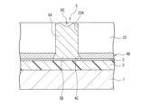
- the probe device 20 includes a glass substrate 1 as a probe device substrate, an elastic material layer 2, a seed layer 3, a wiring pattern 4, a probe 5, and an insulating film 17 (see Figure 11-3).
- Figure 1 shows the probe device 20 in a completed state
- Figures 2 and 3 show the glass substrate 1 in an unfolded state.
- the glass substrate 1 includes a rectangular substrate body 1A and a pair of folded portions 1B.
- the outline of the substrate body 1A determines the outline of the probe device 20 in a plan view.
- the folded portions 1B are elongated rectangular portions having the same width as the substrate body 1A, and are fixed to overlap the rear surfaces of both side portions of the substrate body 1A.
- As the material for the glass substrate it is preferable to use a material having excellent flatness and durability, such as reinforced glass used in displays for electronic devices.
- the elastic material layer 2 is provided in a structure made up of a substrate body 1A and a pair of folded parts 1B, covering the underside of one folded part 1B, through the surface of the substrate body 1A, and over to the underside of the other folded part 1B.
- the cut surfaces 1c at both ends of the substrate body 1A and the outer cut surface 1c of the folded part 1B are arranged to be flush with each other.
- a structure made up of the substrate body 1A and a pair of folded parts 1B is used, but the structure does not have to be configured as described above as long as the wiring pattern 4 (rear electrode pad portion 4B) can be routed on the opposite side of the probe 5 in the probe device 20 via the flexible elastic material layer 2.
- the elastic material layer 2 is made of polyimide.
- the thickness of the elastic material layer 2 can be set to, for example, 3.0 to 50.0 ⁇ m. In this embodiment, the thickness of the elastic material layer 2 is set to 5 ⁇ m.
- the elastic material layer 2 made of polyimide has cushioning properties, flexibility, etc.
- a seed layer 3 made of, for example, nickel or a nickel alloy and having a thickness of, for example, about 50 to 500 nm is formed. Methods for forming this seed layer 3 include sputtering, vapor deposition, and electroless plating.
- Materials other than polyimide include polyamide, polyester, polyethylene, polyvinyl alcohol, polypropylene, polycarbonate, polystyrene, etc.
- a large number of probes 5 are arranged to stand upright at a narrow pitch in a rectangular area in the center of the substrate body 1A.
- each probe 5 is provided on an electrode pad portion (end of a circular shape in a plan view) 4A of an independent wiring pattern 4.
- the height dimension of the probe 5 is set to less than 50 ⁇ m. In the present embodiment, the diameter dimension of the probe 5 is 10 ⁇ m.
- the distance between the paired upright probes 5 is set to be equal to or less than the height of the probe 5. In the present embodiment, the height of the probe 5 is 15 ⁇ m, and the distance between the paired probes 5 is set to 15 ⁇ m.
- the distance (gap dimension) between the paired probes 5 shown in FIG. 4 is set to 5 ⁇ m.
- an insulating film 17 (see FIG. 11-3) having a thickness of, for example, 13 ⁇ m is formed at least in the area where the probes 5 are provided, thereby increasing the strength of the measurement surface side of the probe device 20.
- the exposed height dimension of the probe 5 is set to 7 ⁇ m.
- the underlying seed layer 3 is also formed to the same contour as the wiring pattern 4.
- the wiring pattern 4 and the probe 5 are formed of a nickel-cobalt (Ni-Co) alloy.
- the thickness of the wiring pattern 4 and the electrode pad portion 4A is set to 5 ⁇ m.
- the Vickers hardness of the wiring pattern 4 is 250 to 550 Hv, and the Vickers hardness of the probe 5 is also set to 250 to 550 Hv.
- examples of materials for the wiring pattern include copper (Cu), chromium (Cr), tin (Sn), nickel (Ni), palladium (Pd), and nickel phosphorus (Ni-P).
- the Vickers hardness of each material is known to be 40 to 85 Hv for copper, 800 to 1000 Hv for chromium, 100 to 350 Hv for nickel, 3 to 60 Hv for tin, 300 to 500 Hv for palladium, and 450 to 1000 Hv for nickel phosphorus, and may be appropriately selected according to the required hardness and electrical resistance.
- the Vickers hardness of the probe 5 is preferably higher than that of the wiring pattern 4.
- the electrical resistance of the wiring pattern 4 is preferably lower than that of the probe 5.
- the multiple wiring patterns 4 are drawn out independently from the electrode pad portion 4A arranged in the central region on the substrate body 1A (seed layer 3) to both sides of the substrate body 1A and extend to the surface region of the folded portion 1B.
- the ends of the wiring patterns 4 on the folded portion 1B are the back-side electrode pad portions 4B.
- a circular opening 4C is formed in the center of the electrode pad portion 4A of the wiring pattern 4. The innermost part of this opening 4C faces the underlying seed layer 3.
- a filling portion 5B of a probe 5 is formed in the opening 4C so as to densely penetrate therethrough.
- a cylindrical protrusion 5A is formed on the probe 5 above the filling portion 5B. The protruding portion 5A is set to have a diameter greater than the diameter of the opening 4C so as to cover at least the upper part of the opening 4C.
- the probe 5 penetrating the electrode pad portion 4A of the above structure is firmly fixed at the wide joint surface between the upper surface of the electrode pad portion 4A, the inner surface of the opening 4C, and the seed layer 3. More specifically, as shown in FIG. 5, the filling portion 5B of the probe 5 is joined to the inner peripheral surface (curved surface) 4C1 of the opening 4C with the electrode pad portion 4A in the wiring pattern 4. Also, the upper surface (flat surface) 4A1 around the upper end of the opening 4C in the electrode pad portion 4A is joined to the flange surface (annular flat area at the lower end) 5A1 of the protruding portion 5A in the probe 5.
- the inner peripheral surface 4C1 of the opening 4C is composed of a continuous curved surface surrounding the entire circumference of the filling portion 5B of the probe 5. Also, the lower end surface 5B2 of the filling portion 5B of the probe 5 is joined to the upper surface of the seed layer 3 within the opening 4C. Note that in this embodiment, the planar shape of the opening 4C is circular and the inner peripheral surface 4C1 is composed of a single curved surface that goes around, but the opening 4C may be composed of multiple curved surfaces.
- an electrode pad portion 4A in the wiring pattern 4 that is rectangular in plan view.
- the opening 4C of the electrode pad portion 4A is also rectangular in plan view, and the opening 4C is surrounded by four flat surfaces 4C2.
- the filling portion 5B of the probe 5 (not shown) that fills this opening 4C is formed in a prismatic shape having four side surfaces that join with the four flat surfaces of the opening 4C.
- the upper surface around the upper end of the opening 4C in the electrode pad portion 4A and the flange surface (annular flat surface at the lower end) (not shown) of the protrusion 5A of the probe 5 are joined by flat surfaces.
- the probe 5 is joined to the wiring pattern 4 at one or more curved surfaces, or at least a part of the side of the probe 5 is joined to the wiring pattern 4 at two or more flat surfaces, so that the probe 5 can be prevented from falling off the electrode pad portion 4A or bending.
- the probe 5 when an external stress is applied to the probe 5 having such a fixed structure, the probe 5 has the function of dispersing the external stress to the upper surface of the electrode pad portion 4A, the inner surface of the opening 4C, and the seed layer 3 side.
- the external stress can also be dispersed to the elastic material layer 2, so that the probe 5 can be prevented from falling, falling off, or being damaged when the probe 5 is pressed against the bump 15 during measurement.
- the tip of the probe 5 is formed of a curved surface 5D having a recess 5C in the center of the tip surface.
- the diameter of the probe 5 is set to, for example, about 5.0 to 15.0 ⁇ m.
- the radius of curvature of the recess 5C is set to, for example, 1.0 to 5.0 ⁇ m.
- the radius of curvature of the curved surface of the peripheral shoulder of the recess 5C is set to, for example, 0.1 to 3.0 ⁇ m.
- the substrate 11 to be measured includes a core substrate 12 having a multi-layer structure (not shown), a front surface pad portion 13, a rear surface pad portion 14, and bumps 15.
- the bumps 15 are substantially spherical or cylindrical, and are made of solder. The Vickers hardness of the solder is about 20 Hv.
- the present invention is applied to a substrate 11 to be measured as shown in Figures 6 and 7, but as described above, the present invention can also be applied to various substrates such as package substrates, printed wiring boards, flexible boards, multilayer wiring boards, electrode plates for liquid crystal displays and organic EL displays, and film carriers.
- the elastic material layer 2 made of polyimide is interposed between the glass substrate 1 and the probe 5, so that the elastic material layer 2 can absorb the reaction force when the probe 5 hits the bump 15. This prevents the probe 5 from being deformed so as to tilt, bending, or falling off.
- this embodiment has a simple structure in which the elastic material layer 2 is interposed between the glass substrate 1 side and the probe 5 side, and can simultaneously accommodate miniaturization and narrow pitch of the probe 5 and reduce costs.
- the elastic material layer 2 can absorb variations in height among the plurality of bumps 15, measurement accuracy is high and stable measurement is possible. If the variation in height between the multiple bumps 15 is sufficiently small, or if the bumps 15 can absorb the variation in height by being deformed when the probe 5 comes into contact with them, then the elastic material layer 2 does not need to be provided.
- Figure 8 shows the state in which the probe device 20 and tester 6 according to this embodiment are connected by wiring 7 to perform electrical measurements on the substrate 11 to be measured.
- the tip surface of the probe 5 is formed as a curved surface 5D having a recess 5C, so that the peripheral shoulder of the recess 5C can easily bite into the bump 15 provided on the surface of the substrate 11 to be measured, as shown in Figure 8. This results in good electrical connection between the multiple probes 5 and the corresponding bumps 15, making it possible to stabilize the electrical measurements.
- the tip of the probe 5 is formed with a curved surface 5D that has no edges, which reduces the generation of solder shavings and the like. This prevents solder shavings and the like from adhering to the tip of the probe 5, and makes it easy to maintain the cleanliness of the probe 5 at a high level with simple cleaning. This reduces the occurrence of errors and false detections caused by solder shavings and the like generated by the probe device 20.
- a seed layer 3 made of a nickel alloy and having a thickness of, for example, about 50 to 500 nm is formed by electroless plating on the entire surface of the elastic material layer 2.
- the seed layer 3 may be formed by electroless plating of nickel (Ni).
- the seed layer 3 may be formed by sputtering, vapor deposition, or the like.
- FIG. 9-3 to 11-2 show the probe formation process.
- a positive photoresist 9 is applied on the seed layer 3 and pre-baked.
- a mask pattern is transferred to the photoresist 9 by exposure using a photomask 21.
- a positive photoresist 9 is used, but a negative photoresist can also be used.
- a pattern may be dynamically created by direct exposure using a DMD (Digital Micromirror Device) or the like without using the photomask 21.
- DMD Digital Micromirror Device
- FIG. 10-1 shows a cross section of an area where the electrode pad portions 4A in multiple wiring patterns 4 are arranged adjacent to each other in the center of the glass substrate 1.
- the electrode pad portion 4A is formed on the exposed portion 9B of the photoresist 9 by a first electroforming process.
- FIG. 10-2 shows a cross section of the area where the electrode pad portion 4A is formed, but in this process, the entire wiring pattern 4 including the electrode pad portion 4A is patterned (formed).
- the wiring pattern 4 grows using the underlying seed layer 3 as a seed for film formation.
- the film thickness of the wiring pattern 4 is set to, for example, 5.0 ⁇ m.
- the composition ratio of Ni-Co is adjusted so that the Vickers hardness of the wiring pattern 4 formed by the first electroforming process is 250 to 550 Hv.
- FIG. 10-3 shows the state after the wiring pattern 4 is formed, the remaining portion 9A of the photoresist 9 is peeled off, and then new photoresist 16 is used and exposed and developed to form the remaining portion 16A and the exposed portion 16B.
- the exposed portion 16B becomes the pattern for forming the probe 5. That is, when viewed in a plan view, the opening 4C of the electrode pad portion 4A is set to be located at the center of the exposed portion 16B. The diameter dimension of this exposed portion 16B is set to about 5.0 to 15.0 ⁇ m. Note that since these exposed portions 16B are the pattern for forming the probe 5, they are not formed in other areas of the photoresist 16.
- FIG. 11-1 shows the state in which the probe 5 is formed by the second electroforming process based on the resist pattern formed by the photoresist 16.
- the upper surface (tip surface) of the probe 5 growing in the exposed portion 16B is formed as a curved surface 5D having a recess 5C in the center.
- the diameter of the probe 5 is, for example, about 5.0 to 15.0 ⁇ m.
- the radius of curvature of the recess 5C is, for example, 1.0 ⁇ m to 5.0 ⁇ m.
- the radius of curvature of the curved surface of the peripheral shoulder of the recess 5C is, for example, 0.1 to 3.0 ⁇ m.
- the composition ratio of Ni-Co is adjusted so that the Vickers hardness of the probe 5 formed by the second electroforming process is 250 to 550 Hv.
- FIG. 11-2 shows the state after the remaining portion 16A of the photoresist 16 has been peeled off.
- a probe 5 is formed that is bonded to the seed layer 3, the opening 4C, and the periphery of the opening 4C of the electrode pad portion 4A. Note that in this process, the seed layer 3 in the area excluding the wiring pattern 4 is also etched at the same time.
- an insulating film 17 is formed in the area other than the probe 5 and the back side electrode pad portion 4B (see FIG. 1 to FIG. 3).
- this insulating film 17 By forming this insulating film 17, the measurement surface side of the probe device 20 can be protected. In other words, the strength of the probe 5 can be improved.
- inspection failures caused by contact with the bump 15 can be prevented.
- the insulating film 17 can be formed by forming a nitride film, an oxide film, an SOG (Spin-On-Glass) film, DLC (Diamond Like Carbon), etc. by the CVD method and then etching back to expose the probe 5.
- Glass substrate folding process 12A shows a substrate structure used in a folding process of a glass substrate in a manufacturing method of a probe device according to the present embodiment.
- the insulating film 17 is omitted from the illustration.
- a laser beam LB is irradiated from the glass substrate 1 side to the folded area of the glass substrate 1, causing the interface between the elastic material layer 2 and the glass substrate 1 to peel off.
- the glass substrate 1 in the area where the interface with the elastic material layer 2 has peeled off is cut out and removed.
- the folded portion 1B on which the back side electrode pad portion 4B is formed is in a state where it is connected to the substrate main body 1A via the elastic material layer 2, etc.
- the folded-back portions 1B are folded over and overlapped on the backsides of both sides of the substrate body 1A, completing the probe device 20 as shown in FIG. 1.
- [Second embodiment] 13 shows a probe device 20A according to a second embodiment of the present invention.
- the folded portion 1B in the probe device 20 according to the first embodiment is omitted, and the elastic material layer 2 is folded back and fixed to the back side of the substrate body 1A.
- the other configurations of this embodiment are similar to those of the probe device 20 according to the first embodiment.
- [Third embodiment] 14 shows a probe device 20B according to a third embodiment of the present invention.
- the folded portion 1B in the probe device 20 according to the first embodiment is divided into folded portions 1E and 1F, and the cut surfaces of the substrate body 1D and the folded portions 1E and 1F are cut at an angle of 45 degrees and folded back so that the cut surfaces are joined together.
- the other configurations of this embodiment are similar to those of the probe device 20 according to the first embodiment.
- [Fourth embodiment] 16 is a partial cross-sectional explanatory view showing the main part of a probe device according to a fourth embodiment of the present invention.
- the opening 4C of the electrode pad portion 4A is formed so that the opening diameter gradually increases toward the glass substrate 1 side. Therefore, the inner wall of the opening 4C has a reverse tapered cross section, and the filling portion 5B of the probe 5 filled in the opening 4C is securely held by the electrode pad portion 4A. This provides the effect that the probe 5 is unlikely to fall over or fall off.
- polyimide is applied to the surface of a glass substrate 1 to a thickness of, for example, 3.0 to 50.0 ⁇ m to form an elastic material layer 2.
- a seed layer 3 made of a nickel alloy and having a thickness of, for example, 50 to 500 nm is formed by electroless plating on the entire surface of the elastic material layer 2.
- Nickel (Ni) may be electrolessly plated as the seed layer 3.
- sputtering, vapor deposition, etc. may also be used as a method for forming the seed layer 3.
- the photoresist 22 is patterned (exposed and developed) into a truncated cone shape.
- the photoresist 22 in this truncated cone-shaped portion forms a space for forming the filling portion 5B of the probe 5. While leaving this truncated cone-shaped photoresist 22, a first electroforming is performed to form the wiring layer 4D.
- the photoresist 22 is peeled off to expose the opening 4C in the wiring layer 4D.
- a positive photoresist 23 is applied and pre-baked.
- FIG. 18-1 exposure light is irradiated onto the entire surface from the glass substrate 1 side (backside exposure). Since the exposure light passes through the opening 4C of the wiring layer 4D, the exposed area is removed through development as shown in FIG. 18-2. As shown in FIG. 18-2, the opening 4C and the opening 23A of the photoresist 23 are integrated to form a space for forming the probe 5.
- FIG. 19-1 shows the state in which the second electroforming is performed in the state shown in FIG. 18-2 to form the probe 5. After that, the photoresist 23 is peeled off.
- a new photoresist 24 is patterned so that the probe 5 is covered with the photoresist 24. Then, etching is performed using the pattern of this photoresist 24 as an etching mask to pattern the wiring layer 4D. Note that the etching of the wiring layer 4D may be performed by either dry etching or wet etching.
- [Fifth embodiment] 21 shows a probe device 30 according to a fifth embodiment of the present invention.
- the probe device 30 includes a glass substrate 31 as a probe device substrate, an elastic material layer 32, a plurality of probes 5, a plurality of through holes 34, and a plurality of rear surface side electrode pad portions 36.
- the probes 5 are formed through the steps shown in FIGS. 9-1 to 11-3.
- the through holes 34 can be formed by using, for example, a plating technique as a via filling technique in the substrate.
- the probes 5 are arranged at a narrow pitch so as to correspond to the pitch between the bumps 15 on the substrate 11 to be measured, as shown in FIG. 6, for example.
- the through holes 34 penetrate the glass substrate 31 and connect the wiring pattern 33 formed on the front side of the glass substrate 31 to the rear side wiring pattern 35.
- the rear side electrode pads 36 are connected to the rear side wiring pattern 35.
- the rear side electrode pads 36 are arranged in a region wider than the array region of the probes 5, with a pitch larger than the pitch of the probes 5.
- the pin jig 40 is connected to the back electrode pad portion 36 of the probe device 30 to perform the measurement.
- the pin jig 40 has a jig substrate 41 made of a rectangular insulator of approximately the same size as the glass substrate 31 of the probe device 30, and a plurality of contact pins 42 are provided on the surface of the jig substrate 41 at a pitch corresponding to the back electrode pad portion 36 of the probe device 30.
- the pitch between these contact pins 42 is equal to the pitch between the back electrode pad portions 36 of the probe device 30, and is set to be longer than the pitch between the probes 5.
- the pin jig 40 is connected to a tester 43. This tester 43 can perform a well-known open/short test on the measured substrate.
- the glass substrate 31 is used as the probe device substrate, but a silicon substrate or other insulating substrate may be used.
- the relationship between the probe 5, wiring pattern 33, and elastic material layer 32 in this embodiment is the same as that in the probe device 20 according to the first embodiment. Unlike the probe device 20 according to the first embodiment, this embodiment does not require cutting the glass substrate 31 and bending it to the back side, which makes it easier and more reliable to process.
- the probe device 30A includes a glass substrate 31 as a probe device substrate, a resin-based base material 37 arranged so as to surround the periphery of the glass substrate 31, an elastic material layer 32, a plurality of probes 5, a plurality of through holes 34 formed in the resin-based base material 37, and a plurality of rear surface side electrode pad portions 36.
- the probes 5 are formed through the steps shown in FIGS. 9-1 to 11-3.
- the wiring pattern 33 to which the probes 5 are connected and the back-side wiring pattern 35 connected to the back-side electrode pad portion 36 are connected by a plurality of through holes 34.
- the probes 5 are arranged at a narrow pitch.
- the back-side electrode pad portion 36 is arranged in a region wider than the arrangement region of the probes 5, and is distributed at a pitch larger than the pitch of the probes 5.
- the other configurations of this embodiment are the same as those of the probe device 30 according to the fifth embodiment.
- the relationship between the probes 5, the wiring pattern 33, and the elastic material layer 32 in this embodiment is the same as that of the probe device 20 according to the first embodiment.
- a glass substrate 31 is used as the probe device substrate, but a silicon substrate or other insulating substrate may also be used.
- the through-holes 34 are formed in the resin base material 37 , which has the advantage that the manufacturing process is easier than forming the through-holes 34 in the glass substrate 31 .
- This embodiment is particularly effective when tempered glass is used as the material for the glass substrate 31, since it is difficult to form the through holes 34.
- FIG. 23 shows a probe device 50 according to a seventh embodiment of the present invention.
- This probe device 50 includes a laminated printed wiring board 51 having a plurality of wiring layers and via holes formed therein, an elastic material layer 32, a plurality of probes 5, and a rear surface side electrode pad portion 36.
- the probes 5 are also formed through the steps shown in FIGS. 9-1 to 11-3.
- the laminated printed wiring board 51 can be a printed wiring board made of various materials, such as a glass epoxy board or a glass nonwoven fabric board.
- the laminated printed wiring board 51 is used as the probe device substrate, simply by shifting the positions of the via holes in the laminated printed wiring boards, it becomes easy to create a wiring structure in which the pitch between the back-side electrode pad portions 36 is widened for the probes 5 arranged in a narrow area.
- the wiring can be created in a complex manner within the laminated printed wiring board 51, the pattern configuration of the wiring pattern 33 and the back-side wiring pattern 35 can be simplified. With this probe device 50, too, the pitch of the back-side wiring pattern 35 can be made large, making it possible to reliably connect the pin jig 40.
- a measured substrate 11 having a spherical bump 15 as shown in Figures 6 and 7 is used, but a measured substrate 11A having a cylindrical (rectangular cross-section) bump 15A as shown in Figure 15 may also be used. Even in such other embodiments, the effect of being able to perform measurements reliably is achieved.
- the entire surface of the probe device substrate is covered with the elastic material layer 2, 32, but it is also possible to form a first insulating film made of, for example, an oxide film, a nitride film, SOG, DLC, etc. in the area where the probe 5 is present, and form a second insulating film made of, for example, a resin on the outside of that.
- a first insulating film made of, for example, an oxide film, a nitride film, SOG, DLC, etc.
- a second insulating film made of, for example, a resin on the outside of that.
- the hardness of the first insulating film is greater than the hardness of the second insulating film.
Landscapes
- Physics & Mathematics (AREA)
- General Physics & Mathematics (AREA)
- Engineering & Computer Science (AREA)
- General Engineering & Computer Science (AREA)
- Microelectronics & Electronic Packaging (AREA)
- Testing Or Measuring Of Semiconductors Or The Like (AREA)
- Measuring Leads Or Probes (AREA)
- Geometry (AREA)
- Testing Of Individual Semiconductor Devices (AREA)
Priority Applications (3)
| Application Number | Priority Date | Filing Date | Title |
|---|---|---|---|
| KR1020257039358A KR20260035129A (ko) | 2023-07-07 | 2024-05-22 | 프로브 장치 및 그 제조 방법 |
| JP2025532413A JPWO2025013432A1 (https=) | 2023-07-07 | 2024-05-22 | |
| CN202480042575.1A CN121511409A (zh) | 2023-07-07 | 2024-05-22 | 探针装置及其制造方法 |
Applications Claiming Priority (4)
| Application Number | Priority Date | Filing Date | Title |
|---|---|---|---|
| JP2023-112543 | 2023-07-07 | ||
| JP2023112543 | 2023-07-07 | ||
| JP2023-183975 | 2023-10-26 | ||
| JP2023183975 | 2023-10-26 |
Publications (1)
| Publication Number | Publication Date |
|---|---|
| WO2025013432A1 true WO2025013432A1 (ja) | 2025-01-16 |
Family
ID=94215327
Family Applications (1)
| Application Number | Title | Priority Date | Filing Date |
|---|---|---|---|
| PCT/JP2024/018901 Ceased WO2025013432A1 (ja) | 2023-07-07 | 2024-05-22 | プローブ装置およびその製造方法 |
Country Status (5)
| Country | Link |
|---|---|
| JP (1) | JPWO2025013432A1 (https=) |
| KR (1) | KR20260035129A (https=) |
| CN (1) | CN121511409A (https=) |
| TW (1) | TW202507300A (https=) |
| WO (1) | WO2025013432A1 (https=) |
Citations (6)
| Publication number | Priority date | Publication date | Assignee | Title |
|---|---|---|---|---|
| JPH0463135U (https=) * | 1990-10-03 | 1992-05-29 | ||
| JPH05226430A (ja) * | 1992-02-10 | 1993-09-03 | Nitto Denko Corp | プローブカード構造体およびその製法 |
| JPH06188299A (ja) * | 1992-08-12 | 1994-07-08 | Fujitsu Ltd | 半導体デバイスのチップもしくはマルチチップモジュールのキャリアをテストする方法および装置 |
| JPH0763787A (ja) * | 1993-06-16 | 1995-03-10 | Nitto Denko Corp | プローブ構造 |
| JPH0763788A (ja) * | 1993-08-21 | 1995-03-10 | Hewlett Packard Co <Hp> | プローブおよび電気部品/回路検査装置ならびに電気部品/回路検査方法 |
| JP2003344448A (ja) * | 2002-05-30 | 2003-12-03 | Matsushita Electric Ind Co Ltd | 電圧プローブ、これを用いた半導体装置の検査方法、およびモニタ機能付き半導体装置 |
-
2024
- 2024-05-22 JP JP2025532413A patent/JPWO2025013432A1/ja active Pending
- 2024-05-22 WO PCT/JP2024/018901 patent/WO2025013432A1/ja not_active Ceased
- 2024-05-22 KR KR1020257039358A patent/KR20260035129A/ko active Pending
- 2024-05-22 CN CN202480042575.1A patent/CN121511409A/zh active Pending
- 2024-06-05 TW TW113120841A patent/TW202507300A/zh unknown
Patent Citations (6)
| Publication number | Priority date | Publication date | Assignee | Title |
|---|---|---|---|---|
| JPH0463135U (https=) * | 1990-10-03 | 1992-05-29 | ||
| JPH05226430A (ja) * | 1992-02-10 | 1993-09-03 | Nitto Denko Corp | プローブカード構造体およびその製法 |
| JPH06188299A (ja) * | 1992-08-12 | 1994-07-08 | Fujitsu Ltd | 半導体デバイスのチップもしくはマルチチップモジュールのキャリアをテストする方法および装置 |
| JPH0763787A (ja) * | 1993-06-16 | 1995-03-10 | Nitto Denko Corp | プローブ構造 |
| JPH0763788A (ja) * | 1993-08-21 | 1995-03-10 | Hewlett Packard Co <Hp> | プローブおよび電気部品/回路検査装置ならびに電気部品/回路検査方法 |
| JP2003344448A (ja) * | 2002-05-30 | 2003-12-03 | Matsushita Electric Ind Co Ltd | 電圧プローブ、これを用いた半導体装置の検査方法、およびモニタ機能付き半導体装置 |
Also Published As
| Publication number | Publication date |
|---|---|
| TW202507300A (zh) | 2025-02-16 |
| JPWO2025013432A1 (https=) | 2025-01-16 |
| KR20260035129A (ko) | 2026-03-12 |
| CN121511409A (zh) | 2026-02-10 |
Similar Documents
| Publication | Publication Date | Title |
|---|---|---|
| US7452248B2 (en) | Interconnection device for a printed circuit board, a method of manufacturing the same, and an interconnection assembly having the same | |
| US5042148A (en) | Method of manufacturing a probing card for wafer testing | |
| US6314641B1 (en) | Interconnect for testing semiconductor components and method of fabrication | |
| US8191246B1 (en) | Method of manufacturing a plurality of miniaturized spring contacts | |
| JPH02181946A (ja) | ウエハ試験用探触板 | |
| KR101051136B1 (ko) | 공간 변환기, 공간 변환기를 포함하는 프로브 카드 및 공간변환기의 제조 방법 | |
| JP3924710B2 (ja) | コンタクタ | |
| KR100787160B1 (ko) | 평판표시소자 테스트를 위한 검사장치 및 그 제조방법 | |
| WO2025013432A1 (ja) | プローブ装置およびその製造方法 | |
| WO2006085573A1 (ja) | インターポーザ、プローブカードおよびインターポーザの製造方法 | |
| WO2013084874A1 (ja) | プローブカード用のバンプ付きメンブレンシート、プローブカード及びプローブカード用のバンプ付きメンブレンシートの製造方法 | |
| TW201303309A (zh) | 探針卡及其製作方法 | |
| US20020125901A1 (en) | Probe for inspecting semiconductor device and method of manufacturing the same | |
| KR100830352B1 (ko) | 프로브 팁, 프로브 카드, 프로브 팁 제조 방법 및 프로브구조물 제조 방법 | |
| JP3446607B2 (ja) | コンタクトピン及びコンタクトプローブの製造方法 | |
| KR100799237B1 (ko) | 웨이퍼검사용 프로브핀과 프로브핀바의 조립체 | |
| WO2025173530A1 (ja) | プローブ装置およびその製造方法 | |
| KR100977207B1 (ko) | 프로브 및 프로브 카드의 제조 방법 | |
| KR100827994B1 (ko) | 이종 도금 결합방식을 이용한 하이브리드형 고강도 탐침 구조물 및 그 제작 방법 | |
| KR100842395B1 (ko) | 무전해도금법을 이용한 프로브카드용 탐침구조물 제조 방법 | |
| KR101006929B1 (ko) | 프로브 조립체 | |
| KR101846010B1 (ko) | 영상표시패널 검사용 프로브 유닛의 제작 방법 및 이에 의해 제작된 프로브 유닛 | |
| KR100959797B1 (ko) | 접촉 구조물의 제조 방법 | |
| KR20100060976A (ko) | 프로브 및 프로브 카드의 제조 방법 | |
| TW201407167A (zh) | 刀片狀微探針結構及其製作方法 |
Legal Events
| Date | Code | Title | Description |
|---|---|---|---|
| 121 | Ep: the epo has been informed by wipo that ep was designated in this application |
Ref document number: 24839329 Country of ref document: EP Kind code of ref document: A1 |
|
| ENP | Entry into the national phase |
Ref document number: 2025532413 Country of ref document: JP Kind code of ref document: A |
|
| NENP | Non-entry into the national phase |
Ref country code: DE |