WO2024122296A1 - ビニル化合物、ビニル組成物、ビニル樹脂硬化物、プリプレグ、樹脂付きフィルム、樹脂付き金属箔、金属張積層板およびプリント配線板 - Google Patents
ビニル化合物、ビニル組成物、ビニル樹脂硬化物、プリプレグ、樹脂付きフィルム、樹脂付き金属箔、金属張積層板およびプリント配線板 Download PDFInfo
- Publication number
- WO2024122296A1 WO2024122296A1 PCT/JP2023/041220 JP2023041220W WO2024122296A1 WO 2024122296 A1 WO2024122296 A1 WO 2024122296A1 JP 2023041220 W JP2023041220 W JP 2023041220W WO 2024122296 A1 WO2024122296 A1 WO 2024122296A1
- Authority
- WO
- WIPO (PCT)
- Prior art keywords
- vinyl
- group
- cured product
- resin
- vinyl compound
- Prior art date
- Legal status (The legal status is an assumption and is not a legal conclusion. Google has not performed a legal analysis and makes no representation as to the accuracy of the status listed.)
- Ceased
Links
Images


Classifications
-
- C—CHEMISTRY; METALLURGY
- C07—ORGANIC CHEMISTRY
- C07C—ACYCLIC OR CARBOCYCLIC COMPOUNDS
- C07C69/00—Esters of carboxylic acids; Esters of carbonic or haloformic acids
- C07C69/76—Esters of carboxylic acids having a carboxyl group bound to a carbon atom of a six-membered aromatic ring
- C07C69/94—Esters of carboxylic acids having a carboxyl group bound to a carbon atom of a six-membered aromatic ring of polycyclic hydroxy carboxylic acids, the hydroxy groups and the carboxyl groups of which are bound to carbon atoms of six-membered aromatic rings
-
- B—PERFORMING OPERATIONS; TRANSPORTING
- B32—LAYERED PRODUCTS
- B32B—LAYERED PRODUCTS, i.e. PRODUCTS BUILT-UP OF STRATA OF FLAT OR NON-FLAT, e.g. CELLULAR OR HONEYCOMB, FORM
- B32B15/00—Layered products comprising a layer of metal
- B32B15/04—Layered products comprising a layer of metal comprising metal as the main or only constituent of a layer, which is next to another layer of the same or of a different material
- B32B15/08—Layered products comprising a layer of metal comprising metal as the main or only constituent of a layer, which is next to another layer of the same or of a different material of synthetic resin
-
- B—PERFORMING OPERATIONS; TRANSPORTING
- B32—LAYERED PRODUCTS
- B32B—LAYERED PRODUCTS, i.e. PRODUCTS BUILT-UP OF STRATA OF FLAT OR NON-FLAT, e.g. CELLULAR OR HONEYCOMB, FORM
- B32B15/00—Layered products comprising a layer of metal
- B32B15/14—Layered products comprising a layer of metal next to a fibrous or filamentary layer
-
- B—PERFORMING OPERATIONS; TRANSPORTING
- B32—LAYERED PRODUCTS
- B32B—LAYERED PRODUCTS, i.e. PRODUCTS BUILT-UP OF STRATA OF FLAT OR NON-FLAT, e.g. CELLULAR OR HONEYCOMB, FORM
- B32B27/00—Layered products comprising a layer of synthetic resin
- B32B27/30—Layered products comprising a layer of synthetic resin comprising vinyl (co)polymers; comprising acrylic (co)polymers
-
- B—PERFORMING OPERATIONS; TRANSPORTING
- B32—LAYERED PRODUCTS
- B32B—LAYERED PRODUCTS, i.e. PRODUCTS BUILT-UP OF STRATA OF FLAT OR NON-FLAT, e.g. CELLULAR OR HONEYCOMB, FORM
- B32B5/00—Layered products characterised by the non- homogeneity or physical structure, i.e. comprising a fibrous, filamentary, particulate or foam layer; Layered products characterised by having a layer differing constitutionally or physically in different parts
- B32B5/22—Layered products characterised by the non- homogeneity or physical structure, i.e. comprising a fibrous, filamentary, particulate or foam layer; Layered products characterised by having a layer differing constitutionally or physically in different parts characterised by the presence of two or more layers which are next to each other and are fibrous, filamentary, formed of particles or foamed
- B32B5/24—Layered products characterised by the non- homogeneity or physical structure, i.e. comprising a fibrous, filamentary, particulate or foam layer; Layered products characterised by having a layer differing constitutionally or physically in different parts characterised by the presence of two or more layers which are next to each other and are fibrous, filamentary, formed of particles or foamed one layer being a fibrous or filamentary layer
- B32B5/28—Layered products characterised by the non- homogeneity or physical structure, i.e. comprising a fibrous, filamentary, particulate or foam layer; Layered products characterised by having a layer differing constitutionally or physically in different parts characterised by the presence of two or more layers which are next to each other and are fibrous, filamentary, formed of particles or foamed one layer being a fibrous or filamentary layer impregnated with or embedded in a plastic substance
-
- C—CHEMISTRY; METALLURGY
- C08—ORGANIC MACROMOLECULAR COMPOUNDS; THEIR PREPARATION OR CHEMICAL WORKING-UP; COMPOSITIONS BASED THEREON
- C08F—MACROMOLECULAR COMPOUNDS OBTAINED BY REACTIONS ONLY INVOLVING CARBON-TO-CARBON UNSATURATED BONDS
- C08F12/00—Homopolymers and copolymers of compounds having one or more unsaturated aliphatic radicals, each having only one carbon-to-carbon double bond, and at least one being terminated by an aromatic carbocyclic ring
- C08F12/02—Monomers containing only one unsaturated aliphatic radical
- C08F12/04—Monomers containing only one unsaturated aliphatic radical containing one ring
-
- C—CHEMISTRY; METALLURGY
- C08—ORGANIC MACROMOLECULAR COMPOUNDS; THEIR PREPARATION OR CHEMICAL WORKING-UP; COMPOSITIONS BASED THEREON
- C08F—MACROMOLECULAR COMPOUNDS OBTAINED BY REACTIONS ONLY INVOLVING CARBON-TO-CARBON UNSATURATED BONDS
- C08F12/00—Homopolymers and copolymers of compounds having one or more unsaturated aliphatic radicals, each having only one carbon-to-carbon double bond, and at least one being terminated by an aromatic carbocyclic ring
- C08F12/34—Monomers containing two or more unsaturated aliphatic radicals
-
- C—CHEMISTRY; METALLURGY
- C08—ORGANIC MACROMOLECULAR COMPOUNDS; THEIR PREPARATION OR CHEMICAL WORKING-UP; COMPOSITIONS BASED THEREON
- C08F—MACROMOLECULAR COMPOUNDS OBTAINED BY REACTIONS ONLY INVOLVING CARBON-TO-CARBON UNSATURATED BONDS
- C08F16/00—Homopolymers and copolymers of compounds having one or more unsaturated aliphatic radicals, each having only one carbon-to-carbon double bond, and at least one being terminated by an alcohol, ether, aldehydo, ketonic, acetal or ketal radical
- C08F16/12—Homopolymers and copolymers of compounds having one or more unsaturated aliphatic radicals, each having only one carbon-to-carbon double bond, and at least one being terminated by an alcohol, ether, aldehydo, ketonic, acetal or ketal radical by an ether radical
- C08F16/32—Monomers containing two or more unsaturated aliphatic radicals
-
- C—CHEMISTRY; METALLURGY
- C08—ORGANIC MACROMOLECULAR COMPOUNDS; THEIR PREPARATION OR CHEMICAL WORKING-UP; COMPOSITIONS BASED THEREON
- C08F—MACROMOLECULAR COMPOUNDS OBTAINED BY REACTIONS ONLY INVOLVING CARBON-TO-CARBON UNSATURATED BONDS
- C08F2/00—Processes of polymerisation
- C08F2/44—Polymerisation in the presence of compounding ingredients, e.g. plasticisers, dyestuffs, fillers
-
- C—CHEMISTRY; METALLURGY
- C08—ORGANIC MACROMOLECULAR COMPOUNDS; THEIR PREPARATION OR CHEMICAL WORKING-UP; COMPOSITIONS BASED THEREON
- C08F—MACROMOLECULAR COMPOUNDS OBTAINED BY REACTIONS ONLY INVOLVING CARBON-TO-CARBON UNSATURATED BONDS
- C08F20/00—Homopolymers and copolymers of compounds having one or more unsaturated aliphatic radicals, each having only one carbon-to-carbon double bond, and only one being terminated by only one carboxyl radical or a salt, anhydride, ester, amide, imide or nitrile thereof
- C08F20/02—Monocarboxylic acids having less than ten carbon atoms, Derivatives thereof
- C08F20/10—Esters
-
- C—CHEMISTRY; METALLURGY
- C08—ORGANIC MACROMOLECULAR COMPOUNDS; THEIR PREPARATION OR CHEMICAL WORKING-UP; COMPOSITIONS BASED THEREON
- C08J—WORKING-UP; GENERAL PROCESSES OF COMPOUNDING; AFTER-TREATMENT NOT COVERED BY SUBCLASSES C08B, C08C, C08F, C08G or C08H
- C08J5/00—Manufacture of articles or shaped materials containing macromolecular substances
- C08J5/24—Impregnating materials with prepolymers which can be polymerised in situ, e.g. manufacture of prepregs
-
- H—ELECTRICITY
- H05—ELECTRIC TECHNIQUES NOT OTHERWISE PROVIDED FOR
- H05K—PRINTED CIRCUITS; CASINGS OR CONSTRUCTIONAL DETAILS OF ELECTRIC APPARATUS; MANUFACTURE OF ASSEMBLAGES OF ELECTRICAL COMPONENTS
- H05K1/00—Printed circuits
- H05K1/02—Details
- H05K1/03—Use of materials for the substrate
-
- B—PERFORMING OPERATIONS; TRANSPORTING
- B32—LAYERED PRODUCTS
- B32B—LAYERED PRODUCTS, i.e. PRODUCTS BUILT-UP OF STRATA OF FLAT OR NON-FLAT, e.g. CELLULAR OR HONEYCOMB, FORM
- B32B2457/00—Electrical equipment
- B32B2457/08—PCBs, i.e. printed circuit boards
Definitions
- the present invention relates to vinyl compounds, vinyl compositions, vinyl resin cured products, prepregs, resin-coated films, resin-coated metal foils, metal-clad laminates, and printed wiring boards.
- a well-known example of a printed wiring board with high heat dissipation properties is the so-called thick copper board, which is made by making the copper (i.e. the copper pattern) that forms the circuit thicker than before, allowing more heat to be dissipated through the copper.
- this thick copper board has the problem that it is not suitable for communication devices, which require compactness and light weight, because it is thick overall.
- a known example of a printed wiring board with high heat dissipation properties is a metal-based board, which has a metal plate on one side that allows it to dissipate more heat through the metal plate.
- this metal-based board requires an increased number of manufacturing steps, which increases the manufacturing costs of the communications device.
- materials that contain resin as the main component and have high heat dissipation properties are known to contain a highly thermally conductive filler.
- materials that contain filler have poor processability, which is an issue in that they are not suitable for manufacturing printed wiring boards.
- Patent Document 1 A resin with high thermal conductivity has been disclosed as a material that can solve these problems.
- Electronic materials used in high-speed communication devices are required to have high heat dissipation properties as well as low dielectric loss, and the resin disclosed in Patent Document 1 has high thermal conductivity and low dielectric loss by itself.
- the present invention aims to provide a new compound that is suitable as a constituent material for printed wiring boards and can be used to produce a resin with high thermal conductivity and low dielectric loss.
- Y1 and Y2 are the same or different and each is a group selected from the group consisting of a vinyl group and a vinylbenzyl group;
- Q is any one of groups selected from the group consisting of formulas (1) to (3),
- a 1 , A 2 , A 3 and A 4 are the same or different and each is a substituted or unsubstituted divalent aromatic group (excluding a nitrogen-containing aromatic heterocyclic group); a substituted or unsubstituted divalent cycloalkylene group, a divalent group in which two or more substituted or unsubstituted divalent aromatic groups (excluding nitrogen-containing aromatic heterocyclic groups) are linked by a single bond, a divalent group in which two or more substituted or unsubstituted divalent cycloalkylene groups or cycloalkenylene groups are linked by a single bond, and a divalent group
- a prepreg comprising the vinyl compound or semi-cured product thereof according to any one of [1] to [3], or the vinyl composition or semi-cured product thereof according to [5], and a fibrous base material.
- a resin-coated film comprising a resin layer containing the vinyl compound or semi-cured product thereof according to any one of [1] to [3], or the vinyl composition or semi-cured product thereof according to [5], and a support film.
- a resin-coated metal foil comprising a resin layer containing the vinyl compound or semi-cured product thereof according to any one of [1] to [3], or the vinyl composition or semi-cured product thereof according to [5], and a metal foil.
- a metal-clad laminate comprising an insulating layer containing a cured product of the vinyl compound according to any one of [1] to [3] or a cured product of the vinyl composition according to [5], and a metal foil.
- a metal-clad laminate comprising an insulating layer containing a cured product of the prepreg according to [7] and a metal foil.
- a printed wiring board comprising an insulating layer containing a cured product of the vinyl compound according to any one of [1] to [3] or a cured product of the vinyl composition according to [5], and a conductor wiring.
- a printed wiring board comprising an insulating layer containing a cured product of the prepreg according to [7] and a conductive wiring.
- the present invention provides a novel compound that is suitable as a constituent material for printed wiring boards and can be used to produce resins with high thermal conductivity and low dielectric loss. Furthermore, when producing molded products such as resins and printed wiring boards from the novel compound, the low melting point makes the manufacturing process easier.
- FIG. 1 is a cross-sectional view showing a schematic example of a laminate structure obtained by using a vinyl compound according to one embodiment of the present invention.
- FIG. 2 is a cross-sectional view showing a schematic diagram of another example of a laminate structure obtained by using a vinyl compound according to one embodiment of the present invention.
- FIG. 2 is a cross-sectional view showing a schematic diagram of still another example of a laminate structure obtained by using a vinyl compound according to one embodiment of the present invention.
- FIG. 2 is a cross-sectional view showing a schematic diagram of still another example of a laminate structure obtained by using a vinyl compound according to one embodiment of the present invention.
- the vinyl compound of the present embodiment is represented by the following formula (A):
- the vinyl compound represented by the above formula (A) may be referred to as "vinyl compound (A)".
- Y 1 and Y 2 may be the same or different and each is a group selected from the group consisting of a vinyl group and a vinylbenzyl group.
- the structure of Q is a mesogenic skeleton, and has a structure in which two or more hydrocarbon rings are linked.
- the number of carbon atoms in Q is not particularly limited, but may be 12 or more, for example, and is preferably 13 or more.
- Q is any group selected from the group consisting of formulas (1) to (3),
- a 1 , A 2 , A 3 and A 4 are the same or different and each is a substituted or unsubstituted divalent aromatic group (excluding a nitrogen-containing aromatic heterocyclic group); a substituted or unsubstituted divalent cycloalkylene group, a divalent group in which two or more substituted or unsubstituted divalent aromatic groups (excluding nitrogen-containing aromatic heterocyclic groups) are linked by a single bond, a divalent group in which two or more substituted or unsubstituted divalent cycloalkylene groups or cycloalkenylene groups are linked by a single bond, and a divalent group in which one or more substituted or unsubstituted divalent aromatic groups (excluding nitrogen-containing aromatic heterocyclic groups) and one or more substituted or unsubstituted divalent cycloalkylene groups or cycloalkenylene groups are
- the aromatic ring may be a monocyclic ring, a condensed ring, or a heterocyclic ring, but is preferably a monocyclic ring.
- the heteroatom contained in the heterocyclic ring may be a heteroatom other than a nitrogen atom, such as an oxygen atom or a sulfur atom. From the viewpoint of suppressing dielectric loss or reducing the dielectric tangent, it is preferable that the aromatic ring does not contain a heteroatom.
- the aromatic ring is preferably a monocyclic ring or a condensed ring, and more preferably a monocyclic ring.
- the number of carbon atoms in the unsubstituted divalent aromatic group is not particularly limited, but is preferably 3 to 20, more preferably 6 to 16, and even more preferably 6 to 14.
- unsubstituted divalent aromatic rings include benzene, naphthalene, anthracene, phenanthrene, pyrene, triphenylene, perylene, furan, benzofuran, dibenzofuran, thiophene, benzothiophene, and dibenzothiophene.
- the substituent is preferably a substituent other than a hydroxy group, for example, one or more groups selected from the group consisting of an alkyl group having 1 to 20 carbon atoms and an alkoxy group having 1 to 20 carbon atoms.
- the alkyl group having 1 to 20 carbon atoms includes known alkyl groups.
- the number of carbon atoms in the alkyl group is preferably 1 to 8, and more preferably 1 to 4.
- Specific examples of alkyl groups having 1 to 4 carbon atoms include a methyl group, an ethyl group, an n-propyl group, an isopropyl group, an n-butyl group, a sec-butyl group, a tert-butyl group, and an isobutyl group.
- Alkoxy groups having 1 to 20 carbon atoms include known alkoxy groups.
- the number of carbon atoms in the alkoxy group is preferably 1 to 8, and more preferably 1 to 4.
- Specific examples of alkoxy groups having 1 to 4 carbon atoms include a methoxy group, an ethoxy group, an n-propyloxy group, an isopropyloxy group, an n-butoxy group, a sec-butoxy group, a tert-butoxy group, and an isobutyloxy group.
- the cycloalkane ring and the cycloalkene ring may be a monocyclic ring, a condensed ring, or a heterocyclic ring.
- the heteroatom contained in the heterocyclic ring may be, for example, an oxygen atom, a nitrogen atom, and a sulfur atom. From the viewpoint of suppressing dielectric loss or dielectric tangent, it is preferable that the aromatic ring does not contain a heteroatom.
- the aromatic ring is preferably a monocyclic ring or a condensed ring, and more preferably a monocyclic ring.
- the cycloalkylene group and the cycloalkenylene group may be in a cis form, a trans form, or a mixture thereof, and in the case of a mixture, it is preferable that the proportion of the trans form is higher.
- the number of carbon atoms in the unsubstituted divalent cycloalkylene group and cycloalkenylene group is not particularly limited, but is preferably 3 to 20, more preferably 6 to 16, and even more preferably 6 to 14.
- unsubstituted cycloalkane rings include cyclopropane, cyclobutane, cyclopentane, cyclohexane, cycloheptane, cyclooctane, cyclononane, cyclodecane, cycloundecane, cyclododecane, cyclotridecane, cyclotetradecane, cyclopentadecane, cyclohexadecane, cycloheptadecane, cyclooctadecane, cyclononadecane, cycloicosane, decalin, adamantane, oxetane, tetrahydrofuran, tetrahydropyran, 1,4-dioxane, 1,3-dioxane, aziridine, pyrrolidine, piperidine, piperazine, morpholine, tetrahydrothioph
- unsubstituted cycloalkene ring examples include cyclopropylene, cyclobutene, cyclopentene, cyclohexene, cycloheptene, cyclooctene, cyclononene, and cyclodecene.
- the substituent has the same meaning as the substituent that the divalent aromatic group may have.
- the number of substituted or unsubstituted aromatic rings linked by single bonds is not particularly limited as long as it is two or more, but is preferably 2 to 10, more preferably 2 to 4, and even more preferably 2.
- compounds in which two or more unsubstituted aromatic rings are linked by a single bond include biphenyl, o-terphenyl, m-terphenyl, p-terphenyl, m-quarterphenyl, and p-quarterphenyl.
- the number of substituted or unsubstituted cycloalkane rings or cycloalkene rings linked by single bonds is not particularly limited as long as it is two or more, but is preferably 2 to 10, more preferably 2 to 4, and even more preferably 2.
- cyclopropylcyclohexane bicyclohexyl, 1,3-dicyclohexylcyclohexane, 1,4-dicyclohexylcyclohexane, 1-cyclohexylpyrrolidine, and 4-cyclohexylmorpholine.
- the number of substituted or unsubstituted aromatic rings linked by single bonds is not particularly limited as long as it is 1 or more, but is preferably 1 to 5, more preferably 1 to 3, and even more preferably 1, and the number of substituted or unsubstituted cycloalkane rings or cycloalkene rings linked by single bonds is not particularly limited as long as it is 1 or more, but is preferably 1 to 5, more preferably 1 to 3, and even more preferably 1.
- the total number of substituted or unsubstituted aromatic rings linked by single bonds and the number of substituted or unsubstituted cycloalkane rings or cycloalkene rings is preferably 2 to 10, more preferably 2 to 4, and even more preferably 2.
- compounds in which one or more unsubstituted aromatic rings and one or more unsubstituted cycloalkane or cycloalkene rings are linked by a single bond include cyclopropylbenzene, cyclopentylbenzene, cyclohexylbenzene, 1-cyclohexylnaphthalene, 2-cyclohexylnaphthalene, 2-phenyltetrahydrofuran, 1-phenyladamantane, 1,3-diphenyladamantane, 1,3,5,7-tetraphenyladamantane, 2-cyclohexylfuran, 4-phenylpiperidine, 2-cyclohexylthiophene, and 4-phenylmorpholine, 1,1'-(1-cyclohexene-1,4-diyl)-bisbenzene, and 1-(4-phenyl-1-cyclohexen-1-yl)-3-methylbenzene.
- a substituted or unsubstituted divalent aromatic group is a residue formed by removing two hydrogen atoms from any position of a substituted or unsubstituted aromatic ring.
- a substituted or unsubstituted divalent cycloalkylene group or cycloalkenylene group is a residue formed by removing two hydrogen atoms from any position of a substituted or unsubstituted cycloalkane ring or cycloalkene ring.
- a 1 , A 2 , A 3 and A 4 are preferably divalent aromatic groups (excluding nitrogen-containing aromatic heterocyclic groups).
- X 1 , X 2 and X 3 are the same or different and are any one selected from the group consisting of a single bond, an ester group (*-COO-** or *-OCO-**; * and ** indicate the bonding position with any one of A 1 , A 2 , A 3 and A 4 ), and a carbonyl group, preferably an ester group or a carbonyl group, more preferably an ester group.
- X 1 , X 2 and X 3 are ester groups, a vinyl resin cured material containing a vinyl compound can exhibit excellent heat conductivity.
- n1 and n2 are the same or different and are preferably integers from 1 to 10, more preferably integers from 2 to 8.
- alkyl spacers having n1 and n2 carbon atoms into the vinyl compound in addition to the mesogenic skeleton, it is possible to obtain a vinyl compound with a low melting point.
- the melting point of the vinyl compound (A) is preferably 50 to 150°C or less, more preferably 80 to 140°C or less, even more preferably 90 to 130°C or less, and particularly preferably 95 to 120°C. If the melting point of the vinyl compound is within the above range, processing by melt kneading or the like becomes easy, and the energy required for processing can also be reduced.
- the vinyl compound (A) is polymerizable and can form a vinyl resin cured product (described later) by polymerization (also referred to as "curing" in this specification). Therefore, the vinyl compound (A) can be suitably used to form a constituent material for the insulating layer of a printed wiring board, a heat dissipation material, etc.
- resins that contain hydroxyl groups tend to have high dielectric loss.
- a resin that is a cured product of a compound (monomer) that has epoxy groups at the end has hydroxyl groups in the resin, and its dielectric loss is high.
- the end of vinyl compound (A) is not an epoxy group or a hydroxyl group, but a vinyl group (ethenyl group). Therefore, the cured product (polymer) of vinyl compound (A) has no hydroxyl groups in the resin, and therefore shows low dielectric loss.
- the vinyl compound (A) is, for example, a compound represented by the formula (B): (In the formula, Q has the same meaning as above.) (hereinafter, sometimes referred to as "compound (B)”) represented by formula (C) or formula (D) (wherein Z1 represents a halogen atom, and n represents an integer of 1 to 20). (in this specification, may be referred to as “compound (C)” or “compound (D)”) in the presence of a base.
- Examples of the compound (B) include 1-1'-(1-1'-biphenyl)-4-4'-diyl bis(4-hydroxybenzoate) and (trans-4-(phenylene)cyclohexyl)bis(4-hydroxybenzoate).
- Z1 represents a halogen atom, and examples of the halogen atom include a chlorine atom, a bromine atom, and an iodine atom.
- Examples of compound (C) or compound (D) include 2-vinylbenzyl bromoalkyl ether, 3-vinylbenzyl bromoalkyl ether, 4-vinylbenzyl bromoalkyl ether, chloroalkyl vinyl ether, bromoalkyl vinyl ether, 2-vinylbenzyl chloroalkyl ether, 3-vinylbenzyl chloroalkyl ether, 4-vinylbenzyl chloroalkyl ether, etc.
- Compound (C) and compound (D) may be used alone or in any combination and ratio of two or more kinds.
- the amount of compound (C) or compound (D) used is usually preferably 2 to 100 equivalents, more preferably 2 to 50 equivalents, relative to compound (B).
- the base used in the reaction may be either an inorganic base or an organic base.
- the inorganic base include alkali metal hydrides such as sodium hydride and potassium hydride; alkali metal hydroxides such as sodium hydroxide and potassium hydroxide; and alkali metal carbonates such as sodium carbonate and potassium carbonate.
- the organic base include pyridine.
- the amount of the base used is usually preferably 2 to 5 equivalents relative to compound (B). When an organic base that is liquid under reaction conditions is used, such an organic base may be used in an excess amount to serve as a reaction solvent.
- reaction of compound (B) with compound (C) or compound (D) is usually carried out in a solvent by mixing compound (B), compound (C) or compound (D), and a base.
- the order of mixing is not particularly limited.
- the solvent is not particularly limited as long as it is a solvent inert to the reaction, but a hydrophilic solvent is preferred in that it is easy to suppress the generation of by-products.
- the hydrophilic solvent include alcohol-based solvents such as methanol, ethanol, propanol, butanol, ethylene glycol, and propylene glycol; ketone-based solvents such as methyl ethyl ketone and methyl isobutyl ketone; aprotic polar solvents such as N,N-dimethylformamide, dimethyl sulfoxide, and N-methylpyrrolidone; and ether-based solvents such as tetrahydrofuran, dioxane, methoxymethyl ether, and diethoxyethane, either alone or in mixture.
- the organic base when an organic base that is liquid under reaction conditions is used as a base, the organic base may be used as a reaction solvent.
- the solvent is preferably an ether solvent, an aprotic polar solvent, or a mixture thereof, more preferably an aprotic polar solvent, and particularly preferably N,N-dimethylformamide.
- the amount of the solvent used is preferably 1 to 20 mL, more preferably 2 to 10 mL, per gram of compound (B).
- the reaction between compound (B) and compound (C) or compound (D) may be carried out via a halogen exchange reaction in the presence of a catalyst.
- a catalyst examples include alkali metal halides such as sodium iodide and potassium iodide; and quaternary ammonium halides such as tetrabutylammonium iodide.
- the amount of the catalyst used is usually preferably 0.05 to 1 times by mass, more preferably 0.1 to 0.5 times by mass, based on the amount of compound (B) used.
- the reaction between compound (B) and compound (C) or compound (D) may be carried out in the presence of a polymerization inhibitor.
- a polymerization inhibitor examples include 2,6-di(tert-butyl)-p-cresol.
- the amount of the polymerization inhibitor is usually preferably 0.002 to 0.05 times by mass, more preferably 0.004 to 0.02 times by mass, relative to the amount of compound (C) or compound (D) used.
- the reaction may be carried out under normal pressure conditions or under reduced pressure conditions.
- the reaction temperature is usually preferably 10 to 150°C.
- water may be produced as a by-product as the reaction proceeds. In such cases, it is preferable to carry out the reaction while removing the by-product water from the reaction system, and it is preferable to carry out the reaction at a reaction temperature and pressure at which water is removed azeotropically.
- the reaction time is usually preferably 1 to 24 hours.
- the reaction liquid is cooled, water or a mixed solvent containing water is added, the precipitated solid is filtered off, and if necessary, a known post-treatment operation is carried out once or twice or more times to obtain vinyl compound (A).
- a known post-treatment operation include stirring and washing the solid in water, a mixed solvent containing water, or an organic solvent; extraction of the solution in which the solid is dissolved (liquid separation), etc.
- the obtained vinyl compound (A) may be further purified by a conventional purification means if necessary.
- the structure of the obtained vinyl compound (A) can be confirmed by a known method such as nuclear magnetic resonance (NMR) spectroscopy.
- the vinyl composition of the present embodiment contains a vinyl compound (A).
- the vinyl composition of the present embodiment may be referred to as "vinyl composition (A)".
- the vinyl composition (A) has curability and may contain only the vinyl compound (A), or may contain the vinyl compound (A) and also other components than the vinyl compound (A) within the range that does not impair the effects of the present invention.
- the vinyl compound (A) may be cured by heating or by light irradiation. In the following examples, it is cured by heating. When curing the vinyl compound (A), pressure may be applied to the vinyl compound (A).
- the vinyl compound (A) contained in the vinyl composition (A) may be one kind or two or more kinds.
- the vinyl compounds (A) are preferably a mixture of multiple types of vinyl compounds (A) in which the positions of the vinyl groups in the terminal vinylbenzyl groups are different and the portions other than the vinylbenzyl groups are identical.
- the mole number of vinylbenzyl groups whose vinyl group position is m-position is preferably 30 to 90, more preferably 40 to 90, even more preferably 50 to 90, even more preferably 60 to 80, and particularly preferably 70 to 80.
- the ratio of the mole number of vinylbenzyl groups whose vinyl group position is p-position to the mole number of vinylbenzyl groups whose vinyl group position is m-position is preferably 10/90 to 70/30, more preferably 10/90 to 60/40, even more preferably 10/90 to 50/50, even more preferably 20/80 to 40/60, and particularly preferably 20/80 to 30/70.
- the mixture of vinyl compounds (A) melts at a lower temperature, improving the processability of the vinyl compounds.
- Examples of the other components contained in the vinyl composition (A) include a radical initiator; a filler; an additive; a solvent; a vinyl compound other than the vinyl compound (A) (sometimes referred to as “other vinyl compounds” in this specification); and a resin other than a polymer (cured product) of the vinyl compound (A) (sometimes referred to as "other resins” in this specification).
- the additives include, for example, silane coupling agents, colorants, low stress components, release agents, antioxidants, defoamers, flow control agents, etc.
- radical initiator examples include azo compounds and organic peroxides.
- the filler may, for example, be silica powder such as fused crushed silica powder, fused spherical silica powder, crystalline silica powder, or secondary agglomerated silica powder; metal oxides such as alumina, titanium oxide, zinc oxide, tungsten carbide, or magnesium oxide; glass cloth (glass fiber); carbon fiber; nitrides such as boron nitride, aluminum nitride, silicon nitride, or titanium nitride; silicon carbide; aluminum hydroxide; talc; clay; or mica.
- silica powder such as fused crushed silica powder, fused spherical silica powder, crystalline silica powder, or secondary agglomerated silica powder
- metal oxides such as alumina, titanium oxide, zinc oxide, tungsten carbide, or magnesium oxide
- glass cloth (glass fiber) glass fiber
- carbon fiber carbon fiber
- nitrides such as boron nitride, aluminum nit
- the silane coupling agent may, for example, be ⁇ -glycidoxypropyltrimethoxysilane.
- the colorant may, for example, be carbon black.
- Examples of the low stress component include silicone oil and silicone rubber.
- Examples of the release agent include natural wax, synthetic wax, higher fatty acid, metal salt of higher fatty acid, and paraffin.
- the solvent contained in the vinyl composition (A) may, for example, be a ketone-based solvent such as methyl ethyl ketone or methyl isobutyl ketone; an aprotic polar solvent such as dimethyl sulfoxide or N-methylpyrrolidone; an ester-based solvent such as butyl acetate; a glycol-based solvent such as propylene glycol monomethyl ether; or an aromatic solvent such as toluene.
- a ketone-based solvent such as methyl ethyl ketone or methyl isobutyl ketone
- an aprotic polar solvent such as dimethyl sulfoxide or N-methylpyrrolidone
- an ester-based solvent such as butyl acetate
- a glycol-based solvent such as propylene glycol monomethyl ether
- aromatic solvent such as toluene.
- the other vinyl compound is not particularly limited as long as it has a vinyl group and does not fall under the category of the vinyl compound (A).
- the other resin is not particularly limited as long as it is a resin other than a polymer of the vinyl compound (A).
- the vinyl composition (A) may contain only one type of other component, or two or more types.
- the content of the other components in the vinyl composition (A) can be selected arbitrarily depending on the type of the other components.
- the content ratio of the vinyl compound (A) to the total content of components other than the solvent is preferably 80% by mass or more, and may be, for example, 85% by mass or more, 90% by mass or more, 95% by mass or more, 97% by mass or more, or 99% by mass or more. On the other hand, the ratio is 100% by mass or less.
- the vinyl composition (A) having the ratio of 80% by mass or more has a higher effect obtained by containing the vinyl compound (A).
- the vinyl compound (A) obtained by the above method can be used as the vinyl composition (A) as is.
- the vinyl composition (A) containing the other components can be obtained by mixing the vinyl compound (A) with the other components.
- the vinyl resin cured product of the present embodiment is obtained by curing a vinyl compound (A) or a vinyl composition (A).
- the vinyl resin cured product of this embodiment may be referred to as "vinyl resin cured product (A)".
- the vinyl resin cured product has high thermal conductivity and low dielectric loss due to the use of vinyl compound (A), making it suitable as a constituent material for printed wiring boards, and is particularly suitable as an insulating material for printed wiring boards.
- the vinyl resin cured product has a low melting point, which makes the manufacturing process easier.
- the vinyl resin cured material (A) when the vinyl resin cured material (A) is a cured material of a vinyl compound (A), the vinyl resin cured material (A) may be a cured material of one type of vinyl compound (A) or a cured material of two or more types of vinyl compounds (A).
- the vinyl resin cured material (A) when the vinyl resin cured material (A) is a cured product of the vinyl composition (A), the vinyl resin cured material (A) may be a cured product of one type of vinyl composition (A) or a cured product of a mixture of two or more types of vinyl compositions (A).
- the vinyl resin cured product (A) can be prepared, for example, by filling a mold with the vinyl compound (A) or vinyl composition (A) as is, heating it for a predetermined time to cause primary curing, and then heating it for a predetermined time while applying pressure at a predetermined pressure with a press or the like to cause complete curing; by heating the vinyl compound (A) or vinyl composition (A) as is at a predetermined temperature to cause curing; by pouring a powder of the vinyl compound (A) or vinyl composition (A) as is, or after melting as necessary, into a mold and heating it for a predetermined time while applying pressure at a predetermined pressure with a press or the like; or by heating the vinyl compound (A) or vinyl composition (A) by heating and melting it and pouring it into a mold or the like, and then further pressing the mold.
- It can be manufactured by a method of molding by heating; a method of melting the vinyl compound (A) or the vinyl composition (A) and injecting the resulting melt into a preheated mold to harden; a method of partially hardening the vinyl compound (A) or the vinyl composition (A), grinding the resulting partially hardened product, filling a mold with the resulting powder, and melt-molding the filled powder; a method of dissolving the vinyl compound (A) or the vinyl composition (A) as is or as necessary in a solvent, partially hardening while stirring as necessary, casting the resulting solution, and then drying and removing the solvent by ventilation drying or the like, and heating for a predetermined time while applying a predetermined pressure with a press or the like as necessary.
- the heating temperature (curing temperature) when the vinyl compound (A) or the vinyl composition (A) is heated and cured is not particularly limited, but in order to increase the degree of curing of the vinyl compound (A) or the vinyl composition (A), it is preferably 100°C or higher, and more preferably 140°C or higher. In order to avoid excessive heating, the heating temperature is preferably 200°C or lower.
- the heating time (curing time) when the vinyl compound (A) or the vinyl composition (A) is heated and cured is not particularly limited, but in order to increase the degree of curing of the vinyl compound (A) or the vinyl composition (A), it is preferably 1 hour or more, and more preferably 2 hours or more. In order to avoid unnecessary curing operations, the heating time is preferably 10 hours or less.
- the pressure applied when the vinyl compound (A) or the vinyl composition (A) is pressed and cured is not particularly limited, but in terms of increasing the degree of curing of the vinyl compound (A) or the vinyl composition (A), it is preferably 0.7 MPa or more, and more preferably 1.2 MPa or more. In terms of avoiding excessive pressurization, the pressure applied is preferably 3 MPa or less.
- the thermal diffusivity of the vinyl resin cured product (A) is preferably 1.4 ⁇ 10 -7 m 2 /s or more, more preferably 1.8 ⁇ 10 -7 m 2 /s or more, and even more preferably 1.95 ⁇ 10 -7 m 2 /s or more.
- the upper limit of the thermal diffusivity of the vinyl resin cured product (A) is not particularly limited, and the thermal diffusivity may be 4.0 ⁇ 10 -7 m 2 /s or less, 3.6 ⁇ 10 -7 m 2 /s or less, or 3.2 ⁇ 10 -7 m 2 /s or less.
- the thermal diffusivity of the vinyl resin cured product (A) may be, for example, any one of 1.4 ⁇ 10 ⁇ 7 to 4.0 ⁇ 10 ⁇ 7 m 2 /s, 1.8 ⁇ 10 ⁇ 7 to 3.6 ⁇ 10 ⁇ 7 m 2 /s, and 1.95 ⁇ 10 ⁇ 7 to 3.2 ⁇ 10 ⁇ 7 m 2 /s.
- the thermal diffusivity of the vinyl resin cured material (A) can be measured by temperature wave thermal analysis (TWA) standardized in ISO 22007-3:2008 (for transport analysis type thin films).
- TWA temperature wave thermal analysis
- the dielectric loss tangent of the vinyl resin cured product (A) at a frequency of 100 MHz is preferably 0.005 or less, more preferably 0.0048 or less, and even more preferably 0.0046 or less.
- the lower limit of the dielectric loss tangent of the vinyl resin cured product (A) is not particularly limited, and the dielectric loss tangent may be 0.001 or more, 0.002 or more, or 0.003 or more.
- the dielectric loss tangent of the vinyl resin cured material (A) at a frequency of 100 MHz may be, for example, any one of 0.001 to 0.005, 0.002 to 0.0048, and 0.003 to 0.0046, although these are only examples of the dielectric loss tangent of the vinyl resin cured material (A).
- the dielectric loss tangent of the vinyl resin cured material (A) at a frequency of 100 MHz can be measured by a capacitance method using an impedance analyzer under the following conditions. Measurement method: Capacitance method Electrode type: 16453A Measurement environment: 23°C, 50% RH Applied voltage: 1V
- the prepreg of the present embodiment comprises a vinyl compound (A) or a semi-cured product thereof, or a vinyl composition (A) or a semi-cured product thereof, and a fibrous base material.
- the prepreg of this embodiment may be referred to as "prepreg (A)".
- a laminate or the like can be easily manufactured by a normal method.
- a desired laminate can be obtained by stacking a plurality of prepregs (A) to form a laminate, and molding and integrating the laminate by applying pressure while heating.
- a printed wiring board (resin layer in the printed wiring board) obtained by using the prepreg (A) or the laminate has high thermal conductivity and low dielectric loss due to the use of the vinyl compound (A).
- the prepreg (A) can be produced by coating or impregnating a fibrous substrate with a solution of the vinyl compound (A) dissolved in a solvent, or by coating or impregnating a fibrous substrate with the vinyl composition (A) or a dilution of the vinyl composition (A) diluted with a solvent, and then heating the coated or impregnated fibrous substrate to semi-cure the vinyl compound (A) or vinyl composition (A).
- the heating temperature (semi-curing temperature) and heating time (semi-curing time) when semi-curing the vinyl compound (A) or the vinyl composition (A) can be appropriately set in consideration of the above-mentioned curing conditions (heating temperature and heating time) of the vinyl compound (A) or the vinyl composition (A) so that the vinyl compound (A) or the vinyl composition (A) does not completely cure.
- the fibrous substrate is not particularly limited as long as it is a fibrous substrate, and may be any known substrate. More specific examples of fibrous substrates include woven and nonwoven fabrics of inorganic fibers such as glass fibers, and woven and nonwoven fabrics of organic fibers such as polyester.
- the resin-attached film of this embodiment comprises a resin layer containing a vinyl compound (A) or a semi-cured product thereof, or a vinyl composition (A) or a semi-cured product thereof, and a support film. More specifically, the resin-attached film of this embodiment may be, for example, a resin-attached film comprising the resin layer and the support film provided on one or both sides of the resin layer.
- a laminate sheet is obtained by using a plurality of resin-attached films of this embodiment, removing the support film, stacking them together to form a laminate, and molding and integrating this laminate by heating and pressing.
- the resin layer in the resin-attached film of this embodiment and the printed wiring board (resin layer in the printed wiring board) obtained using the resin layer or laminate sheet have high thermal conductivity and low dielectric loss due to the use of the vinyl compound (A).
- the support film may be, for example, a polyethylene terephthalate (PET) film.
- PET polyethylene terephthalate
- these support films may be the same as each other or different from each other.
- it means that at least one of the material and thickness of the two layers of support films is different from each other.
- the resin-coated film of this embodiment can be produced by applying a solution of vinyl compound (A) dissolved in a solvent to the support film, or by applying vinyl composition (A) or a dilution of vinyl composition (A) diluted with a solvent to the support film, and then heating the layer of the coating to semi-cure the vinyl compound (A) or vinyl composition (A) in the coating.
- the conditions for semi-cure of vinyl compound (A) or vinyl composition (A) at this time are the same as those for producing the prepreg described above.
- the resin-attached metal foil of this embodiment comprises a resin layer containing a vinyl compound (A) or a semi-cured product thereof, or a vinyl composition (A) or a semi-cured product thereof, and a metal foil. More specifically, the resin-attached metal foil of this embodiment may comprise, for example, the resin layer and the metal foil provided on one or both sides of the resin layer. For example, the resin-attached metal foil of this embodiment may be used to further cure the semi-cured product to form a cured product, and the metal foil may be patterned to form a circuit, thereby forming a printed wiring board.
- the resin-attached metal foil of this embodiment may be used to pattern the metal foil to form a circuit, and resin layers having such circuits may be laminated together with the circuit orientation aligned, and the semi-cured product may be further cured by applying pressure while heating, thereby forming a multilayer printed wiring board having a resin layer containing a cured product of the vinyl compound (A) or a cured product of the vinyl composition (A) as an insulating layer.
- the resin layer in the resin-coated metal foil of this embodiment and the printed wiring board (resin layer in the printed wiring board) obtained using the resin-coated metal foil have high thermal conductivity and low dielectric loss due to the use of the vinyl compound (A).
- the metal foil may be, for example, a copper foil.
- these metal foils may be the same or different from each other.
- it means that at least one of the material and the thickness of the two layers of metal foil is different from each other.
- the resin-coated metal foil of this embodiment can be manufactured in the same manner as the resin-coated film, except that the metal foil is used instead of the support film.
- the metal-clad laminate of this embodiment comprises an insulating layer containing a cured product of a vinyl compound (A), a cured product of a vinyl composition (A), or a cured product of a prepreg (A), and a metal foil. More specifically, the metal-clad laminate of this embodiment may be, for example, a metal-clad laminate comprising the insulating layer and the metal foil provided on one or both sides of the insulating layer. The metal-clad laminate of this embodiment can be made into a printed wiring board by, for example, patterning the metal foil therein to form a conductor wiring (circuit).
- a multi-layer printed wiring board can be made by stacking such a plurality of printed wiring boards via a separately prepared insulating layer and applying pressure while heating.
- the insulating layer in the metal-clad laminate of this embodiment and the printed wiring board obtained using the metal-clad laminate (the insulating layer in the printed wiring board) have high thermal conductivity and low dielectric loss due to the use of the vinyl compound (A).
- the metal foil provided in the metal-clad laminate of this embodiment is the same as the metal foil provided in the resin-coated metal foil described above.
- these metal foils may be the same as each other or different from each other.
- the insulating layer used separately when laminating the printed wiring board may be a known one, the resin layer in the resin-attached film described above, or the laminate sheet which is a laminate of a plurality of the resin layers, or the prepreg (A) described above, or the laminate obtained by overlapping a plurality of prepregs (A).
- the insulating layer may be the resin layer, laminate sheet, prepreg (A), or laminate obtained by further curing the vinyl compound (A) or vinyl composition (A).
- the metal-clad laminate of the present embodiment can be produced, for example, by laminating a metal foil on one or both sides of a prepreg (A) and pressurizing the resulting laminate while heating it, thereby further curing the vinyl compound (A) or a semi-cured product thereof, or the vinyl composition (A) or a semi-cured product thereof in the prepreg (A) to form a cured product, thereby forming an insulating layer and fusing the prepreg (A) and the metal foil.
- the metal-clad laminate of the present embodiment may be produced, for example, by producing a prepreg (A) using the vinyl compound (A) or the vinyl composition (A) by the method described above, and then using this prepreg (A) by the method described above.
- the metal-clad laminate of the present embodiment can also be produced, for example, by heating the above-mentioned resin-attached metal foil to further cure the vinyl compound (A) or a semi-cured product thereof, or the vinyl composition (A) or a semi-cured product thereof in the resin layer, thereby forming an insulating layer containing a cured product of the vinyl compound (A) or a cured product of the vinyl composition (A).
- the printed wiring board of this embodiment comprises an insulating layer containing a cured product of a vinyl compound (A), a cured product of a vinyl composition (A), or a cured product of a prepreg (A), and a conductor wiring. More specifically, the printed wiring board of this embodiment may be, for example, a printed wiring board comprising the insulating layer and the conductor wiring provided on one or both sides of the insulating layer.
- a multi-layer printed wiring board can be formed by stacking a plurality of printed wiring boards of this embodiment via a separately prepared insulating layer and applying pressure while heating.
- the printed wiring board of this embodiment (the insulating layer in the printed wiring board) has high thermal conductivity and low dielectric loss due to the use of the vinyl compound (A).
- the material of the conductor wiring is the same as the metal of the metal foil included in the above-mentioned metal-clad laminate.
- the insulating layer used separately when laminating the printed wiring board of this embodiment is the insulating layer described above. In the case where conductor wiring is provided on both sides of an insulating layer in a printed wiring board, the material and thickness of these conductor wirings may be the same as or different from each other.
- the printed wiring board of this embodiment can be produced, for example, by patterning the metal foil in the above-mentioned metal-clad laminate to form conductor wiring (circuits).
- the printed wiring board of the present embodiment can also be produced by, for example, heating the above-mentioned resin-attached metal foil to further cure the vinyl compound (A) or a semi-cured product thereof, or the vinyl composition (A) or a semi-cured product thereof in the resin layer, thereby forming an insulating layer containing a cured product of the vinyl compound (A) or a cured product of the vinyl composition (A), and then patterning the metal foil to form conductor wiring (circuits).
- the metal foil can be patterned by known methods such as etching.
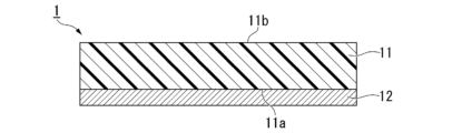
- FIG. 1 is a cross-sectional view showing a schematic example of a laminated structure of the present embodiment obtained using vinyl compound (A). Note that the figures used in the following explanation may show enlarged essential parts for the sake of convenience in order to make the features of the present invention easier to understand, and the dimensional ratios of each component may not necessarily be the same as in reality.
- the laminated structure 1 shown here is configured to include a first layer 11 and a second layer 12 provided on one surface 11a of the first layer 11.
- the first layer 11 is a layer obtained using a vinyl compound (A).
- the second layer 12 is selected according to the type of laminated structure 1. Both the first layer 11 and the second layer 12 are in the form of a film or sheet.
- the second layer 12 may be provided over the entire area of one surface 11a of the first layer 11, or may be provided in a partial area.
- the laminated structure 1 is a resin-attached film.
- the laminate structure 1 is a resin-coated metal foil.
- the laminate structure 1 is a metal-clad laminate.
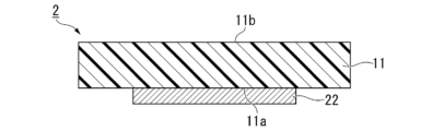
- FIG. 2 is a cross-sectional view showing a schematic diagram of another example of the laminated structure of this embodiment obtained using vinyl compound (A). Note that in FIG. 2 and subsequent figures, components that are the same as those shown in figures that have already been described are given the same reference numerals as in those figures, and detailed descriptions thereof will be omitted.
- the laminated structure 2 shown here is configured to include a first layer 11 and a second layer 22 provided on one surface 11a of the first layer 11.
- the second layer 22 is linear, and in FIG. 2, the cross section of the laminated structure 2 is formed to include a cross section along the linear length direction of the second layer 22.
- the number of linear second layers 22 may be one or may be two or more.
- the laminated structure 2 is the same as the laminated structure 1 shown in FIG. 1, except that the laminated structure 2 includes a linear second layer 22 instead of the film-like second layer 12.
- the laminate structure 2 is a printed wiring board.
- Both the laminated structure 1 and the laminated structure 2 shown in Figures 1 and 2 have nothing on the other surface 11b of the first layer 11, but may have a layer similar to the second layer 12 or the second layer 22.
- FIG. 3 is a cross-sectional view that illustrates still another example of the laminate structure of the present embodiment obtained by using the vinyl compound (A).
- the laminated structure 3 shown here is configured to include a first layer 11, a second layer 12 provided on one surface 11a of the first layer 11, and a third layer 13 provided on the other surface 11b of the first layer 11.
- the third layer 13 is in the form of a film or sheet, and is selected according to the type of the laminated structure 1, similar to the second layer 12.
- the arrangement of the third layer 13 on the other surface 11b of the first layer 11 is similar to the arrangement of the second layer 12 on the one surface 11a of the first layer 11.
- the composition, shape, thickness, and size of the third layer 13 may be the same as or different from the composition, shape, thickness, and size of the second layer 12.
- the third layer 13 may be provided over the entire area of the other surface 11b of the first layer 11, or may be provided in a partial area.
- the laminated structure 3 is a resin-attached film.
- the laminated structure 3 is a resin-coated metal foil.
- the laminated structure 3 is a metal-clad laminate.
- FIG. 4 is a cross-sectional view that illustrates still another example of the laminate structure of the present embodiment obtained by using the vinyl compound (A).
- the laminated structure 4 shown here is configured to include a first layer 11, a second layer 22 provided on one surface 11a of the first layer 11, and a third layer 23 provided on the other surface 11b of the first layer 11.
- the third layer 23 is linear, and in FIG. 4, the cross section of the laminated structure 4 is formed to include both a cross section along the linear length direction of the second layer 22 and a cross section along the linear length direction of the third layer 23.
- the arrangement of the third layer 23 on the other surface 11b of the first layer 11 is similar to the arrangement of the second layer 22 on one surface 11a of the first layer 11.
- the composition, length, thickness, and number of the third layer 23 may be the same as or different from the composition, length, thickness, and number of the second layer 22.
- the number of linear third layers 23 may be one or more.
- the laminated structure 4 is a printed wiring board.
- the conditions for measuring the melting point of vinyl compounds are shown below.
- a glass pan filled with a vinyl compound was heated under the following conditions using a differential scanning calorimeter (FP84HT manufactured by METTLER TLEDO), and the endothermic peak temperature was taken as the melting point.
- FP84HT manufactured by METTLER TLEDO
- the endothermic peak temperature on the lower side was taken as the melting point.
- the test conditions for the cured product are as follows.
- (1) Thermal Diffusivity The thermal diffusivity was measured by the TWA method using a thermal diffusivity measuring device "ai-phase mobile" (manufactured by ai-phase Corporation).
- Example 1 A 300 mL four-neck flask equipped with a thermometer, a condenser, and a stirrer was charged with 8.8 g of sodium hydride and washed with hexane, and then 90 mL of THF, 0.2 g of 2,6-di(tert-butyl)-p-cresol, 6-chloro-1-hexanol, and 18.5 g of 4-vinylbenzyl chloride were charged and reacted at an internal temperature of about 60° C. for 3 hours.
- Example 2 A 200 mL four-neck flask equipped with a thermometer, a condenser, and a stirrer was charged with 4.8 g of sodium hydride, 0.1 g of 2,6-di(tert-butyl)-p-cresol, 12.0 g of vinylbenzyl chloride (a mixture of m,p positional isomers), and 90 mL of dehydrated N,N-dimethylformamide, and the inside temperature was cooled to about 0° C. A solution of 9.8 g of 3-chloro-1-propanol in dehydrated N,N-dimethylformamide was added dropwise, and the mixture was allowed to react at room temperature for 3 hours.
- Example 3 In a 200 mL four-neck flask equipped with a thermometer, a condenser, and a stirrer, 2.5 g of (trans-4-(phenylene)cyclohexyl)bis(4-hydroxybenzoate), 0.03 g of 2,6-di(tert-butyl)-p-cresol, 5.1 g of potassium carbonate, 0.5 g of sodium iodide, 23 mL of N,N-dimethylformamide, and 14.7 g of the chloro compound were charged and reacted for 22 hours at an internal temperature of about 60 to 80° C. After the reaction was completed, the mixture was cooled to room temperature.
- Example 4 In a 500 mL four-neck flask equipped with a thermometer, a condenser and a stirrer, 19.0 g of (trans-4-(phenylene)cyclohexyl)bis(4-hydroxybenzoate), 42.0 g of potassium carbonate, 1.8 g of sodium iodide, 250 mL of N,N-dimethylformamide and 26.5 g of 2-chloroethyl vinyl ether were charged and reacted for 12 hours at an internal temperature of about 60°C. After the reaction was completed, the mixture was cooled to room temperature, 250 mL of water was added, and the precipitated solid was collected by filtration.
- the obtained solid was washed with 50 wt% methanol water and isopropyl alcohol, and dried under reduced pressure to obtain 25.8 g of vinyl compound 4. Purity: 97.7% (LC area percentage value). The melting point of vinyl compound 4 measured by the above method was 128°C.
- Reference Example 1 In a 200 mL four-neck flask equipped with a thermometer, a condenser and a stirrer, 6.0 g of 4,4'-dihydroxy-2,2',3,3',5,5'-hexamethylbiphenyl, 0.06 g of 2,6-di(tert-butyl)-p-cresol, 12 g of potassium carbonate, 1.3 g of sodium iodide, 34 mL of N,N-dimethylformamide and 10 g of 4-vinylbenzyl chloride were charged and reacted for 3 hours at an internal temperature of about 60°C.
- Example 5 to 7 and Comparative Example 1 the vinyl compounds prepared in Examples 1 to 4 and Reference Example 1 shown in Table 1 were placed in the plate-shaped hollow portion of a mold, heated under reduced pressure at the primary curing temperature shown in Table 1 for 1 hour, and then heated at 180°C for 2 hours while applying a pressure of 1.5 MPa to obtain cured products.
- the melting points of the vinyl compounds and the thermal diffusivities of the cured products are shown in Table 1.
- the present invention can be used for printed wiring boards in communication devices, and is particularly suitable for use in printed wiring boards in which the communication devices handle large amounts of data and are expected to generate a large amount of heat.
Landscapes
- Chemical & Material Sciences (AREA)
- Organic Chemistry (AREA)
- Chemical Kinetics & Catalysis (AREA)
- Health & Medical Sciences (AREA)
- Medicinal Chemistry (AREA)
- Polymers & Plastics (AREA)
- Engineering & Computer Science (AREA)
- Materials Engineering (AREA)
- Manufacturing & Machinery (AREA)
- Microelectronics & Electronic Packaging (AREA)
- Addition Polymer Or Copolymer, Post-Treatments, Or Chemical Modifications (AREA)
- Organic Low-Molecular-Weight Compounds And Preparation Thereof (AREA)
- Laminated Bodies (AREA)
Priority Applications (2)
| Application Number | Priority Date | Filing Date | Title |
|---|---|---|---|
| KR1020257018435A KR20250120284A (ko) | 2022-12-09 | 2023-11-16 | 비닐 화합물, 비닐 조성물, 비닐 수지 경화물, 프리프레그, 수지 구비 필름, 수지 구비 금속박, 금속 피복 적층판 및 프린트 배선판 |
| CN202380074323.2A CN120019087A (zh) | 2022-12-09 | 2023-11-16 | 乙烯基化合物、乙烯基组合物、乙烯基树脂固化物、预浸料、带树脂的膜、带树脂的金属箔、覆金属层叠板和印刷线路板 |
Applications Claiming Priority (2)
| Application Number | Priority Date | Filing Date | Title |
|---|---|---|---|
| JP2022-197047 | 2022-12-09 | ||
| JP2022197047A JP2024082874A (ja) | 2022-12-09 | 2022-12-09 | ビニル化合物、ビニル組成物、ビニル樹脂硬化物、プリプレグ、樹脂付きフィルム、樹脂付き金属箔、金属張積層板およびプリント配線板 |
Publications (1)
| Publication Number | Publication Date |
|---|---|
| WO2024122296A1 true WO2024122296A1 (ja) | 2024-06-13 |
Family
ID=91379292
Family Applications (1)
| Application Number | Title | Priority Date | Filing Date |
|---|---|---|---|
| PCT/JP2023/041220 Ceased WO2024122296A1 (ja) | 2022-12-09 | 2023-11-16 | ビニル化合物、ビニル組成物、ビニル樹脂硬化物、プリプレグ、樹脂付きフィルム、樹脂付き金属箔、金属張積層板およびプリント配線板 |
Country Status (5)
| Country | Link |
|---|---|
| JP (1) | JP2024082874A (https=) |
| KR (1) | KR20250120284A (https=) |
| CN (1) | CN120019087A (https=) |
| TW (1) | TW202436279A (https=) |
| WO (1) | WO2024122296A1 (https=) |
Families Citing this family (1)
| Publication number | Priority date | Publication date | Assignee | Title |
|---|---|---|---|---|
| JP2025075531A (ja) * | 2023-10-31 | 2025-05-15 | 住友化学株式会社 | ビニル化合物、ビニル組成物、ビニル樹脂硬化物、プリプレグ、樹脂付きフィルム、樹脂付き金属箔、金属張積層板、及びプリント配線板 |
Citations (16)
| Publication number | Priority date | Publication date | Assignee | Title |
|---|---|---|---|---|
| JPH06148889A (ja) * | 1992-11-13 | 1994-05-27 | Fuji Photo Film Co Ltd | ポジ型感光性組成物 |
| JPH07258638A (ja) * | 1994-02-23 | 1995-10-09 | Merck Patent Gmbh | 液晶状物質 |
| JPH08245520A (ja) * | 1995-03-03 | 1996-09-24 | F Hoffmann La Roche Ag | 光架橋性ナフタレン誘導体 |
| JPH08277247A (ja) * | 1995-03-29 | 1996-10-22 | Merck Patent Gmbh | 反応性ターフェニル化合物 |
| JPH11148079A (ja) * | 1997-11-18 | 1999-06-02 | Dainippon Ink & Chem Inc | 液晶組成物及びこれを用いた光学異方体 |
| JPH11513360A (ja) * | 1994-03-11 | 1999-11-16 | ビーエーエスエフ アクチェンゲゼルシャフト | 新規な重合可能な液晶化合物 |
| JP2002520472A (ja) * | 1998-07-14 | 2002-07-09 | ロリク アーゲー | 組成物 |
| JP2004204190A (ja) * | 2002-12-26 | 2004-07-22 | Chisso Corp | 光重合性液晶組成物および液晶フィルム |
| JP2005035985A (ja) * | 2003-06-23 | 2005-02-10 | Chisso Corp | 液晶性化合物、液晶組成物およびそれらの重合体 |
| US20100059709A1 (en) * | 2006-12-22 | 2010-03-11 | Rolic Ag | Patternable liquid crystal polymer comprising thio-ether units |
| WO2018016640A1 (ja) * | 2016-07-21 | 2018-01-25 | 三菱瓦斯化学株式会社 | 化合物、樹脂、組成物並びにレジストパターン形成方法及び回路パターン形成方法 |
| WO2018079449A1 (ja) * | 2016-10-27 | 2018-05-03 | 富士フイルム株式会社 | 感活性光線性又は感放射線性樹脂組成物、レジスト膜、パターン形成方法、電子デバイスの製造方法 |
| CN111258122A (zh) * | 2020-03-10 | 2020-06-09 | Tcl华星光电技术有限公司 | 液晶材料、液晶显示面板的制作方法及液晶显示面板 |
| WO2020138147A1 (ja) * | 2018-12-28 | 2020-07-02 | 三菱瓦斯化学株式会社 | 化合物、樹脂、組成物、レジストパターンの形成方法、回路パターン形成方法、及び精製方法 |
| WO2020158931A1 (ja) * | 2019-01-31 | 2020-08-06 | 三菱瓦斯化学株式会社 | 化合物、樹脂、組成物、レジストパターン形成方法、回路パターン形成方法及び樹脂の精製方法 |
| CN111690159A (zh) * | 2020-06-10 | 2020-09-22 | 北京大学 | 基于乙烯基醚液晶/高分子全聚合量子点薄膜的制备方法 |
Family Cites Families (1)
| Publication number | Priority date | Publication date | Assignee | Title |
|---|---|---|---|---|
| TWI631167B (zh) | 2017-12-25 | 2018-08-01 | 財團法人工業技術研究院 | 單體、樹脂組合物、膠片、與銅箔基板 |
-
2022
- 2022-12-09 JP JP2022197047A patent/JP2024082874A/ja active Pending
-
2023
- 2023-11-16 KR KR1020257018435A patent/KR20250120284A/ko active Pending
- 2023-11-16 CN CN202380074323.2A patent/CN120019087A/zh active Pending
- 2023-11-16 WO PCT/JP2023/041220 patent/WO2024122296A1/ja not_active Ceased
- 2023-11-29 TW TW112146433A patent/TW202436279A/zh unknown
Patent Citations (16)
| Publication number | Priority date | Publication date | Assignee | Title |
|---|---|---|---|---|
| JPH06148889A (ja) * | 1992-11-13 | 1994-05-27 | Fuji Photo Film Co Ltd | ポジ型感光性組成物 |
| JPH07258638A (ja) * | 1994-02-23 | 1995-10-09 | Merck Patent Gmbh | 液晶状物質 |
| JPH11513360A (ja) * | 1994-03-11 | 1999-11-16 | ビーエーエスエフ アクチェンゲゼルシャフト | 新規な重合可能な液晶化合物 |
| JPH08245520A (ja) * | 1995-03-03 | 1996-09-24 | F Hoffmann La Roche Ag | 光架橋性ナフタレン誘導体 |
| JPH08277247A (ja) * | 1995-03-29 | 1996-10-22 | Merck Patent Gmbh | 反応性ターフェニル化合物 |
| JPH11148079A (ja) * | 1997-11-18 | 1999-06-02 | Dainippon Ink & Chem Inc | 液晶組成物及びこれを用いた光学異方体 |
| JP2002520472A (ja) * | 1998-07-14 | 2002-07-09 | ロリク アーゲー | 組成物 |
| JP2004204190A (ja) * | 2002-12-26 | 2004-07-22 | Chisso Corp | 光重合性液晶組成物および液晶フィルム |
| JP2005035985A (ja) * | 2003-06-23 | 2005-02-10 | Chisso Corp | 液晶性化合物、液晶組成物およびそれらの重合体 |
| US20100059709A1 (en) * | 2006-12-22 | 2010-03-11 | Rolic Ag | Patternable liquid crystal polymer comprising thio-ether units |
| WO2018016640A1 (ja) * | 2016-07-21 | 2018-01-25 | 三菱瓦斯化学株式会社 | 化合物、樹脂、組成物並びにレジストパターン形成方法及び回路パターン形成方法 |
| WO2018079449A1 (ja) * | 2016-10-27 | 2018-05-03 | 富士フイルム株式会社 | 感活性光線性又は感放射線性樹脂組成物、レジスト膜、パターン形成方法、電子デバイスの製造方法 |
| WO2020138147A1 (ja) * | 2018-12-28 | 2020-07-02 | 三菱瓦斯化学株式会社 | 化合物、樹脂、組成物、レジストパターンの形成方法、回路パターン形成方法、及び精製方法 |
| WO2020158931A1 (ja) * | 2019-01-31 | 2020-08-06 | 三菱瓦斯化学株式会社 | 化合物、樹脂、組成物、レジストパターン形成方法、回路パターン形成方法及び樹脂の精製方法 |
| CN111258122A (zh) * | 2020-03-10 | 2020-06-09 | Tcl华星光电技术有限公司 | 液晶材料、液晶显示面板的制作方法及液晶显示面板 |
| CN111690159A (zh) * | 2020-06-10 | 2020-09-22 | 北京大学 | 基于乙烯基醚液晶/高分子全聚合量子点薄膜的制备方法 |
Also Published As
| Publication number | Publication date |
|---|---|
| TW202436279A (zh) | 2024-09-16 |
| KR20250120284A (ko) | 2025-08-08 |
| CN120019087A (zh) | 2025-05-16 |
| JP2024082874A (ja) | 2024-06-20 |
Similar Documents
| Publication | Publication Date | Title |
|---|---|---|
| CN115348977A (zh) | 硬化性树脂、硬化性树脂组合物及硬化物 | |
| TWI496806B (zh) | Epoxy resin compositions, prepregs and such hardened materials | |
| CN100506810C (zh) | 环氧化合物和通过固化所述化合物得到的固化环氧树脂 | |
| JP5382761B2 (ja) | エポキシ樹脂、エポキシ樹脂組成物、これを用いたプリプレグ及び積層板 | |
| JP6429569B2 (ja) | エポキシ樹脂組成物及びその硬化物 | |
| KR20220152203A (ko) | 말레이미드 수지 및 그의 제조 방법, 말레이미드 용액, 그리고, 경화성 수지 조성물 및 그의 경화물 | |
| WO2024122296A1 (ja) | ビニル化合物、ビニル組成物、ビニル樹脂硬化物、プリプレグ、樹脂付きフィルム、樹脂付き金属箔、金属張積層板およびプリント配線板 | |
| JP2021130743A (ja) | 硬化性樹脂組成物、及び、硬化物 | |
| WO2024122295A1 (ja) | ビニル化合物、ビニル組成物、ビニル樹脂硬化物、プリプレグ、樹脂付きフィルム、樹脂付き金属箔、金属張積層板、及びプリント配線板 | |
| JP2024060593A (ja) | ビニル化合物、ビニル組成物、ビニル樹脂硬化物、プリプレグ、樹脂付きフィルム、樹脂付き金属箔、金属張積層板、及びプリント配線板 | |
| JP2010163540A (ja) | エポキシ樹脂組成物及びその硬化物 | |
| JP5188868B2 (ja) | エポキシ樹脂組成物 | |
| JP2025075531A (ja) | ビニル化合物、ビニル組成物、ビニル樹脂硬化物、プリプレグ、樹脂付きフィルム、樹脂付き金属箔、金属張積層板、及びプリント配線板 | |
| JP2012121962A (ja) | エポキシ樹脂組成物、プリプレグおよびそれらの硬化物 | |
| JP7829310B2 (ja) | ビニル化合物、ビニル化合物の製造方法、ビニル組成物、ビニル樹脂硬化物、プリプレグ、樹脂付きフィルム、樹脂付き金属箔、金属張積層板およびプリント配線板 | |
| JP2012111927A (ja) | 組成物及び該組成物を硬化して得られる硬化物 | |
| JP2012107168A (ja) | 組成物及び該組成物を硬化して得られる硬化物 | |
| JP7781429B2 (ja) | 高分子化合物、樹脂組成物、樹脂フィルム、プリプレグ、積層板、プリント配線板、及び半導体パッケージ | |
| CN101171279A (zh) | 环氧树脂、其制造方法及其用途 | |
| JP2003286315A (ja) | 硬化性樹脂組成物及び積層板 | |
| JP2004175950A (ja) | 熱硬化性樹脂組成物 | |
| JP2026005514A (ja) | フェノキシ樹脂 |
Legal Events
| Date | Code | Title | Description |
|---|---|---|---|
| 121 | Ep: the epo has been informed by wipo that ep was designated in this application |
Ref document number: 23900417 Country of ref document: EP Kind code of ref document: A1 |
|
| WWE | Wipo information: entry into national phase |
Ref document number: 202380074323.2 Country of ref document: CN |
|
| WWP | Wipo information: published in national office |
Ref document number: 202380074323.2 Country of ref document: CN |
|
| NENP | Non-entry into the national phase |
Ref country code: DE |
|
| WWP | Wipo information: published in national office |
Ref document number: 1020257018435 Country of ref document: KR |
|
| 122 | Ep: pct application non-entry in european phase |
Ref document number: 23900417 Country of ref document: EP Kind code of ref document: A1 |