WO2024075171A1 - 光送信器 - Google Patents
光送信器 Download PDFInfo
- Publication number
- WO2024075171A1 WO2024075171A1 PCT/JP2022/037035 JP2022037035W WO2024075171A1 WO 2024075171 A1 WO2024075171 A1 WO 2024075171A1 JP 2022037035 W JP2022037035 W JP 2022037035W WO 2024075171 A1 WO2024075171 A1 WO 2024075171A1
- Authority
- WO
- WIPO (PCT)
- Prior art keywords
- optical modulator
- driver
- optical
- subcarrier
- chip
- Prior art date
- Legal status (The legal status is an assumption and is not a legal conclusion. Google has not performed a legal analysis and makes no representation as to the accuracy of the status listed.)
- Ceased
Links
Images




Classifications
-
- G—PHYSICS
- G02—OPTICS
- G02F—OPTICAL DEVICES OR ARRANGEMENTS FOR THE CONTROL OF LIGHT BY MODIFICATION OF THE OPTICAL PROPERTIES OF THE MEDIA OF THE ELEMENTS INVOLVED THEREIN; NON-LINEAR OPTICS; FREQUENCY-CHANGING OF LIGHT; OPTICAL LOGIC ELEMENTS; OPTICAL ANALOGUE/DIGITAL CONVERTERS
- G02F1/00—Devices or arrangements for the control of the intensity, colour, phase, polarisation or direction of light arriving from an independent light source, e.g. switching, gating or modulating; Non-linear optics
- G02F1/01—Devices or arrangements for the control of the intensity, colour, phase, polarisation or direction of light arriving from an independent light source, e.g. switching, gating or modulating; Non-linear optics for the control of the intensity, phase, polarisation or colour
- G02F1/015—Devices or arrangements for the control of the intensity, colour, phase, polarisation or direction of light arriving from an independent light source, e.g. switching, gating or modulating; Non-linear optics for the control of the intensity, phase, polarisation or colour based on semiconductor elements having potential barriers, e.g. having a PN or PIN junction
- G02F1/017—Structures with periodic or quasi periodic potential variation, e.g. superlattices, quantum wells
Definitions
- This disclosure relates to an optical transmitter used in optical communications. More specifically, it relates to an implementation form of an optical transmitter that includes a semiconductor optical modulator and its driver IC.
- an optical transceiver in which an optical receiver and an optical transmitter are integrated is used.
- broadband analog components such as radio frequency (RF) electrical circuits are required.
- RF radio frequency
- an optical modulator requires a modulation bandwidth of 40 GHz or more.
- HB-CDM High-Bandwidth Coherent Driver Modulator
- ICR Integrated Coherent Receiver
- semiconductor-based optical modulators are attracting attention as an alternative to conventional lithium niobate (LN) optical modulators due to their compact size and low cost.
- Compound semiconductors such as InP are mainly used for faster modulation operations.
- Si-based optical devices Furthermore, in systems where compact size and low cost are important, research and development is focused on Si-based optical devices.
- the semiconductor optical modulators mentioned above have their own advantages and disadvantages specific to each material.
- temperature control of the optical modulator chip is essential during operation in order to control the band-edge absorption effect.
- a Si optical modulator has the advantage of not needing temperature control, but has a smaller electro-optic effect than other material systems. This makes it necessary to lengthen the electro-optic interaction length, which can result in increased high-frequency loss as a result of the device length increasing.
- the operating temperature (case temperature) of an optical transmitter using HB-CDM must be in the range of at least -5°C to 75°C. In order to ensure this operating temperature, it has been common to only mount the optical modulator chip on a Peltier element, taking into account power consumption (Patent Document 1).
- this disclosure provides a new configuration and implementation form of an optical transmitter that suppresses the temperature dependency of an optical transmitter including a driver IC, has excellent high-speed performance, and is capable of stable operation regardless of the environmental temperature.
- One aspect of the present disclosure is an optical transmitter that includes a Peltier element, an optical modulator, and a driver integrated circuit (IC) that supplies a modulated electrical signal for the optical modulator, with the optical modulator and the driver IC flip-chip mounted face-down on the top surface of the Peltier element.
- IC driver integrated circuit
- This disclosure makes it possible to realize a new configuration and implementation form for an optical transmitter that suppresses the temperature dependency of the optical transmitter including the driver IC, has excellent speed, and is capable of stable operation regardless of the environmental temperature.
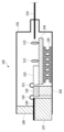
- FIG. 1 is a cross-sectional side view of a prior art HB-CDM optical transmitter.
- 1 is a side cross-sectional view of an optical transmitter using HB-CDM according to an embodiment of the present disclosure.
- 1 is a side cross-sectional view of an optical transmitter using HB-CDM according to another embodiment of the present disclosure.
- 1A and 1B are diagrams for explaining limitations on the height direction of wire connection points and limitations on the spacing between a driver IC and an optical modulator chip 103 in an optical transmitter according to an embodiment of the present disclosure.
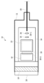
- FIG. 13 is a top view of an optical transmitter using HB-CDM according to another embodiment of the present disclosure.
- 1A and 1B are diagrams illustrating restrictions on pad positions, etc., on the circuit surface of an optical transmitter according to an embodiment of the present disclosure.
- 1A and 1B are diagrams illustrating the density arrangement of Peltier elements in an optical transmitter according to an embodiment of the present disclosure.
- This disclosure presents new configurations for improving the temperature dependency of the high-frequency characteristics of an optical transmitter in which a modulator and its driver IC are integrated into a package, and implementation forms compatible with each configuration.
- the configuration for improving the temperature dependency includes a new use of a temperature regulator (TEC: ThermoElectric Cooler) in the optical transmitter.
- TEC ThermoElectric Cooler
- various implementation forms of the driver IC, optical modulator chip, and spatial optical components compatible with the new use of the TEC are also proposed.
- TECs are also known as thermoelectric coolers, and are known as small cooling devices that use Peltier junctions. TECs are made up of n-type semiconductors, p-type semiconductors, and metals, and when a direct current is passed through both sides of the plate-shaped element, heat is absorbed on one side and dissipated on the other. Reversing the direction of the current switches between heat absorption and dissipation, allowing for localized and precise temperature control of ICs and electronic components. For simplicity's sake, in the following explanation, the temperature regulator will be referred to as a TEC and described as a Peltier element. Any device that can control the temperature of a driver IC or optical modulator chip is not limited to one that uses a Peltier element.
- FIG. 1 is a side cross-sectional view showing the implementation of an optical transmitter using HB-CDM, a conventional technology.
- the optical transmitter 100 contains a driver IC 102, an optical modulator chip 103, and lenses 112 and 113, which are spatial optical components, inside a package housing 101 made of ceramic, metal, or a combination of these. More specifically, the optical modulator chip 103 is mounted on the bottom inside the package housing 101 via a subcarrier 104 on a Peltier element 105. The right end of the optical modulator chip 103 in the drawing has an output facet for modulated light, and lenses 112 and 113 for optically coupling the modulated light to an optical fiber 114 are also mounted on the subcarrier.
- a driver IC 102 is mounted on a metal block or ceramic material 106 adjacent to the optical modulator chip 103.
- the package housing 101 has a wiring board base 107 and a package wall 108 as the left wall in the drawing, which, together with the package housing 101, separate the outside from the internal space of the optical transmitter.
- the optical transmitter 100 can also be constructed so that the entire package is airtight.
- the modulated electrical signal supplied from an external digital signal processor (DSP) is supplied to the optical modulator chip 103 via the wiring layer 109 and driver IC 102 of the wiring board base 107.
- the wiring layer 109 and the driver IC 102, and the driver IC 102 and the optical modulator chip 103 are connected by gold wires 110, 111, etc., respectively.
- the modulated electrical signal includes an I channel and a Q channel for each of the X polarization and the Y polarization.
- one channel is supplied as an electrical signal in a differential signal format, at least eight signal wirings and a GND wiring are required for one optical modulator, but the modulated signal format is not limited to this.
- the optical transmitter 100 shown in FIG. 1 can be mounted on a common device substrate together with an ICR package in which a TIA and an optical receiver on the receiving side are integrated, and a DSP, to form an optical transmitting and receiving device.
- the Peltier element 105 in the optical transmitter. Temperature control is essential for the optical modulator chip 103 fabricated on an InP substrate, and the Peltier element 105 controls the temperature to a predetermined operating temperature. As shown in FIG. 1, the Peltier element 105 has a size that covers at least the entire area of the optical modulator chip 103, and its position may overlap the area of spatial optical components such as lenses.
- the optical transmitter 100 of the conventional technology it was considered that temperature control of the driver IC 102 was not necessary, and it was fixed in the package by a member 106 such as a metal block or ceramic. If the external temperature (ambient temperature) of the optical transmitter 100 rises, the increased temperature becomes the operating temperature of the driver IC 102.
- the driver IC is also a heat source, so considering the heat generated by the driver, it is estimated that the operating temperature of the driver IC is about +5 to +10°C higher than the external temperature. If the maximum environmental temperature of the optical transmitting and receiving device including the optical transmitter is 85°C, the temperature of the driver IC 102 itself will be at least 85°C or higher. The driver IC also consumes a large amount of power, and the driver IC itself generates heat. This means that the backside temperature of the driver IC will exceed the maximum environmental temperature of 85°C due to the heat generated by the driver IC.
- the driver IC has temperature-dependent amplification characteristics (high frequency characteristics) of high frequency electrical signals, and at high temperatures the high frequency band tends to decrease compared to room temperature. Conversely, at low temperatures the high frequency band tends to increase compared to room temperature. Thus, the high frequency characteristics of the driver IC differ between low and high temperatures.
- the modulation signal supplied to the driver IC is optimized and compensated in various ways by the DSP at room temperature. However, dynamically updating such compensation in line with temperature fluctuations is a complex process and is not generally implemented. Because operation continues at a constant compensation state at room temperature, the compensation state of the modulation signal deviates from the optimal point when the state changes to a low or high temperature. This causes fluctuations and deterioration in the optical transmission characteristics and waveform quality of the optical transmitter.
- the IQ modulator of the optical modulator chip 103 is a linear modulator that preserves the amplitude and phase of the electrical signal, and fluctuations in the level and waveform quality of the modulated electrical signal directly affect the quality of the modulated output light. If the external temperature changes while the optical transmitter is in operation, the optical modulator chip itself is maintained at a constant temperature because it is temperature-controlled by a Peltier element, but the operating temperature of the driver IC changes. As a result, fluctuations in the level and quality of the HB-CDM modulated light occur, and temporal changes in the environmental temperature can cause deterioration and instability in the transmission characteristics.
- the deterioration of characteristics due to the environmental temperature on the high frequency side of the electrical signal causes waveform distortion of the modulated signal, degrading the modulation accuracy of the modulated output light from the optical modulator.
- a floor appears in the BER characteristics, leading to a deterioration in the transmission characteristics of the system.
- This disclosure presents a new configuration and implementation form that improves the temperature dependency of high frequency characteristics and optical transmission characteristics in an optical transmitter in which an optical modulator and its driver IC are packaged together.
- FIG. 2 is a side cross-sectional view showing an optical transmitter using HB-CDM according to an embodiment of the present disclosure.
- an InP optical modulator chip 13 its driver IC 12, and other components are integrated inside a package housing 11 along the HB-CDM, similar to the configuration of the conventional optical transmitter 100 shown in FIG. 1.
- the package housing 11 has a wiring board base 18 and a package wall 19 as the wall on the left side of the drawing, and the configuration for dividing the inside and outside of the package is also similar.
- the difference from the conventional configuration of FIG. 1 is the use of the TEC, i.e., the Peltier element, which performs temperature control.
- the driver IC 12 is also mounted on the same Peltier element 16 as the optical modulator chip 13 and the lenses 23 and 24, which are optical mounting members. This makes it possible to control the temperature of the driver IC as well.
- the driver IC 12, optical modulator chip 13, and lenses 23 and 24 are mounted on the Peltier element 16 via the subcarrier 14.
- the subcarrier 14 functions as a base for fixing and holding the driver IC, optical modulator chip, and spatial optical components.
- the subcarrier 14 has wiring for connecting to the DC wiring of the optical modulator chip, RF lines for connecting the driver IC and optical modulator chip, and even positioning markers for mounting the spatial optical components, formed by metal patterns 15.
- the material of the subcarrier 14 is preferably one with excellent thermal conductivity, since it will be equipped with the driver IC 12 and optical modulator chip 13, which are the targets of temperature control.
- a ceramic substrate such as an AlN substrate is preferable.
- the material constant of the AlN substrate is close to that of InP, so it is also compatible with the InP optical modulator in terms of behavior with respect to temperature changes.
- the ceramic on the upper surface of the Peltier element 16 is made of AlN.
- a metal with excellent thermal conductivity, such as CuW, may be used as the material of the subcarrier 14.
- a wiring board is placed on at least a part of the upper surface of the subcarrier as an alternative to the metal pattern 15 on which the above-mentioned RF lines and positioning markers are formed, and the RF lines and positioning markers are formed on the wiring board.
- the Peltier element 16 and the subcarrier 14 are joined with an adhesive or the like that has low thermal resistance and high thermal conductivity. Specifically, it is desirable to mount the subcarrier 14 on the top surface of the Peltier element 16 using a paste or solder with excellent thermal conductivity of 30 W/(mK) or more.
- the subcarrier 14 is depicted as being made of a single layer of AlN, but it can also be a multi-layer AlN substrate.
- a multi-layer substrate By using a multi-layer substrate, it is possible to implement a flexible element and wiring layout that makes full use of multi-layer wiring when there are a large number of DC wirings to the optical modulator or when cross wiring is required to change the order of the terminals. From the perspective of RF design, multi-layer wiring also makes it possible to provide a GNG on the back side of the wiring, which increases the freedom of the wiring layout, such as narrowing the width of each wiring or wiring at a high density, and is extremely effective.
- the driver IC 12 and the optical modulator chip 13 are flip-chip mounted face-down using pillars or bumps, or a combination of these with solder.
- the driver IC 12 and the optical modulator chip 13 are placed on a metal pattern 15 formed on the surface of the subcarrier 14, with the circuit surface (face) on which the electrode pads are formed of the main surface facing the bottom surface of the package housing 11 (i.e., with the surface on which the electrode pads are formed facing downwards).
- the pillars can be, for example, Au pillars or Cu pillars.
- the gap between the driver IC 12 and the optical modulator chip 13 mounted face-down by flip-chip mounting and the subcarrier 14, which is equivalent to the height of the Au pillar or bump, is filled with an underfill material 17 with excellent thermal conductivity.
- an underfill material with a thermal conductivity of 3 W/(mK) or more.
- the underfill material is a dielectric material and has a certain dielectric constant and dielectric tangent, which may lead to loss in high-frequency wiring such as the optical modulator. Please note that depending on the high-frequency band and baud rate required for the optical modulator, it is possible to prioritize high-frequency characteristics over temperature stability and bond strength and not use the underfill material.
- the driver IC is a heating element and was not considered to be a target for temperature control by a Peltier element. Driving power is required to operate the Peltier element, and no consideration was given to using extra power for a heating element.
- the inventors came up with the new idea of adding temperature control to the heating element.
- the optical transmitter 10 disclosed herein is capable of simultaneously controlling the temperature of the optical modulator chip 13 and the driver IC 12 using a single Peltier element 16. Although not shown in FIG. 2, the Peltier element 16 is connected to a control current source. As for the specific control temperatures of each part, it is generally desirable to use an InP optical modulator at around 45 ⁇ 10°C, since the modulation efficiency decreases if the temperature is too low.
- the Peltier element 16 only needs to be controlled at any temperature between 25°C and 50°C, which is a temperature at which the characteristics of the InP optical modulator in the optical modulator chip 13 do not deteriorate significantly and the characteristics of the driver IC can be fully brought out.
- All spatial optical components such as lenses 23 and 24 for optically coupling modulated light with optical fiber 25 are mounted on the Peltier element 16 to suppress the thickness variation of the adhesive caused by temperature changes. This makes it possible to minimize the variation of the optical insertion loss caused by the optical axis shifting due to temperature changes.
- the spatial optical components also include a member for fixing the fiber and a polarization beam combiner (PBC). In order to align the position of the lenses 23 and 24 with the optical axis of the light output from the optical modulator chip 13 flip-chip mounted face-down, the portion of the subcarrier 14 on which the optical components are mounted is made thin.
- FIG. 3 shows a modified form of the optical transmitter 10, which is configured with a subcarrier 14-1 carrying the optical modulator chip 13 and the driver IC 12, and a subcarrier 14-2 carrying the lenses 23 and 24.
- the subcarrier 14-2 may be omitted, and the lenses 23 and 24 may be mounted directly on a TEC such as a Peltier element 16.
- an optical transmitter 10 in HB-CDM form is shown as an example, but similar effects can be obtained with other package forms as long as the optical transmission module is an integrated configuration of a driver IC and optical modulator.
- an example is shown in which wiring from a DSP that supplies a modulation signal to the driver IC 12 is connected by a flexible printed circuit board (FPC) on an RF terrace. That is, the metal pattern 20 formed on the wiring layer on the top surface of the wiring board base 18 on the outside of the optical transmitter is connected to an FPC cable (not shown).
- FPC flexible printed circuit board
- the FPC interface has superior high-frequency characteristics because it does not require RF vias (VIAs), etc.
- the electrode pads of the driver IC 12 and the electrode pads of the optical modulator chip 13 are connected by high-frequency wiring of the metal pattern 15 of the subcarrier 14 made of an AlN substrate by flip-chip mounting using pillars or bumps, or a combination of them and solder.
- flip-chip mounting is difficult between the electrode pads of the driver IC 12 and the electrode pads of the metal pattern 20 on the RF terrace, they are connected by wire lines 21.
- the inductance between the driver IC 12 and the optical modulator chip 13 is what contributes most to the high-frequency characteristics. For example, if the wire is long, the series inductance component increases, and the roll-off frequency in the high-frequency characteristics shifts to the low-frequency side due to LC resonance. Therefore, in order to expand the high-frequency characteristics of the driver IC and improve the quality of the modulated high output, it is desirable for the inductance of the wire to be low.
- the driver IC 12 and the optical modulator chip 13 are connected by flip-chip mounting.
- the inductance of the wire connection between the electrode pad of the driver IC 12 and the electrode pad of the metal pattern 20 on the RF terrace has a small effect on the high-frequency characteristics, it is desirable for the inductance to be as small as possible. Therefore, regulations are established regarding the height and planar directions of the wire connection part.
- Figure 4 is a diagram explaining the height restriction of the wire connection point in the optical transmitter 10 and the restriction of the distance between the driver IC and the optical modulator chip 103.
- the electrodes of the metal pattern 20 of the RF terrace, the driver IC 12, and the vicinity of the upper surface of the optical modulator chip 13 are shown enlarged in the height direction.
- the inductance between the electrodes of the metal pattern of the RF terrace and the electrodes of the driver IC has a smaller effect on the characteristics than the inductance between the electrodes of the driver IC and the electrodes of the optical modulator, it is desirable to make it as small as possible.
- the difference in height between the upper surface of the electrode of the RF terrace connected by the wire line 21 and the upper surface of the metal pattern 15 of the subcarrier 14 100 ⁇ m or less.
- This restriction is the minimum range that can be realized, taking into account the variation in thickness of the driver IC and the variation in the mounting materials of the subcarrier 14.
- the height of the Peltier element 16 may be changed, the thickness of the subcarrier 14 may be changed, or the height of the RF terrace of the wiring board base 18 made of ceramic may be changed.
- the difference in height between the upper surface of the electrode of the RF terrace and the upper surface of the metal pattern 15 of the subcarrier 14 is not necessarily required.
- the upper surface of the electrode of the RF terrace and the upper surface of the metal pattern 15 of the subcarrier 14 may be configured to be at the same height.
- the longer the wiring length the greater the wiring loss and the more the high frequency characteristics deteriorate. It is desirable to make the distance between the driver IC 12 and the optical modulator chip 13 short. However, if the driver IC 12 and the optical modulator chip 13 are too close, the temperature control of the driver IC 12 and the optical modulator chip 13 by one Peltier element 16 may not work sufficiently, or the heat of the driver IC may be transferred to the optical modulator chip, which may cause the operation of the optical transmitter 10 to become unstable. Therefore, it is desirable to separate the driver IC 12 and the optical modulator chip 13 by at least 500 ⁇ m.
- the distance between the driver IC 12 and the optical modulator chip 13 5 mm or less.
- the length of the RF wiring connecting the electrode pads of the optical modulator chip 13 and the electrode pads of the driver IC 12 is 500 ⁇ m or more and 5 mm or less.
- FIG. 5 is a top view showing a modified embodiment of the mounting form of the optical transmitter of the present invention. It corresponds to a top view of the circuit surface inside the module, with the package housing 11 of the optical transmitter 10 shown in FIG. 2 cut away.
- grooves 30-1 and 30-2 are formed on the top surface of the subcarrier 14, as shown by the dotted lines.
- the high-frequency wiring of the subcarrier 14 is configured in an area 33 shown by the dotted line between the driver IC 12 and the optical modulator chip 13.
- the driver IC 12 and the optical modulator chip 13 have electrode pads for RF connection formed around them.
- a linear groove 30-2 is formed only on one side of the high-frequency wiring region 33 for the driver IC 12, and a rectangular groove 30-1 is formed near the periphery 4 of the optical modulator chip 13.
- the shape of the groove is not limited to the configuration shown in FIG. 5, and can be changed according to the properties of the underfill material 17 and the shape of the wiring on the subcarrier 14 that should be avoided.
- the groove 30-2 on the driver IC 12 side is only on one side on the optical modulator chip 13 side, but it may be formed in a rectangular shape at a position corresponding to the periphery 4 of the driver IC.
- FIG. 5 In addition to the configuration of FIG.
- a linear groove may be added to the position on the RF terrace side of the driver IC 12, that is, on one side on the wiring board base 18 side. Furthermore, in FIG. 5, a rectangular groove 30-1 is formed at a position corresponding to the periphery 4 of the optical modulator chip 13, but the groove may be formed only at a position corresponding to two sides on the driver IC 12 side and the lenses 23 and 24 side described below.
- the linear groove 30-2 on the driver IC 12 side and the rectangular groove 30-1 on the optical modulator chip 13 side, that on the driver IC side, also serve as a thermal isolation groove between the optical modulator chip and the driver IC. That is, a groove can be provided on the surface of the subcarrier 14 near at least one of the opposing sides of the driver IC 12 and the optical modulator chip 13. If the subcarrier 14 is composed of a multilayer board, high-frequency wiring can be formed on the inner layer, so a groove can also be formed in the region 33. By forming a groove on at least one of the upper or lower surfaces of the subcarrier 14 between the driver IC 12 and the optical modulator chip 13, this groove can also serve as a thermal isolation groove.
- the underfill material rises up near the chip end face on the lens side of the optical modulator chip 13, the underfill material may adhere to the emission end face and deteriorate the optical coupling with the lenses 23 and 24.
- the groove on one side of the rectangular groove 30-1 on the optical modulator chip 13 side on the lens 23 side shown in FIG. 45 is also effective in avoiding such optical coupling problems.
- the subcarrier 14 is formed in a multi-layer structure, it is possible to avoid the effects of the above-mentioned underfill material by configuring the high-frequency line as an inner layer of the subcarrier. Also, if the high-frequency wiring is configured as an inner layer, a groove can be formed at any location on the top surface of the subcarrier between the optical modulator chip and the driver IC. It goes without saying that sufficient consideration must be given to the effects on disconnection of the inner layer wiring and characteristic impedance. On the other hand, when designing high-frequency wiring with the same line impedance, the signal line width becomes narrower in the inner layer wiring due to the influence of the effective dielectric constant of the subcarrier. Furthermore, since it is also affected by the dielectric loss tangent of the subcarrier, it is desirable to have the wiring pattern on the outermost surface of the subcarrier 14 when only considering the loss of the high-frequency line.
- the lenses 23 and 24 are arranged on the opposite side of the optical modulator chip 13 from the driver IC 12.
- at least one lens may be arranged on the upper or lower side of the optical modulator chip 13 when viewed from the top view of FIG. 5.
- the PBC may be arranged on a side different from the driver IC 12 of the optical modulator chip 13.
- the spatial optical components are mounted above the Peltier element 16 on a side different from the side of the optical modulator chip 13 facing the driver IC 12.
- a groove for allowing excess underfill material to escape may be formed near the side of the optical modulator chip that corresponds to the spatial optical components.
- Figure 6 is a diagram explaining the limitations of pads etc. on the circuit surface of an optical transmitter, as viewed from the subcarrier 14 side.
- Figure 6 shows an electrode pad 26 on the output side of the driver IC 12 and an electrode pad 27 on the input side of the optical modulator chip 13.
- pillars and solder 30 and 31 for flip-chip connection with the metal pattern 15 formed on the surface of the subcarrier 14 are formed on the electrode pads 26 and 27, respectively.
- the electrode pad 26 on the output side of the driver IC 12 is configured as GSGSG
- the electrode pad 27 on the input side of the optical modulator chip 13 is configured as GSSG.
- differential driving is more preferable than single-ended driving
- the optical modulator chip 13 is also differentially driven due to the connectivity with the driver IC 12 that drives differentially.
- a differential line such as a GSGSG or GSSG configuration is also laid out as RF wiring in the metal pattern 15 formed on the surface of the subcarrier 14. If the differential line includes a bent portion, the characteristics tend to deteriorate. Therefore, in this embodiment, as shown in FIG.
- the position of the electrode pad 26 on the output side of the driver IC 12 and the position and channel pitch of the electrode pad 27 on the input side of the optical modulator chip 13 are not significantly shifted so that the RF wiring, i.e., the differential line, is formed in a straight line.
- the differential line is shown by a dashed line.
- the metal pattern 15 may be provided with differential lines that include bends or taper shapes that do not significantly degrade the characteristics of the differential lines.
- lenses 23 and 24 are implemented as spatial optical components, but this also includes fiber fixing members, PBC, etc.
- FIG. 7 is a diagram illustrating the density arrangement of Peltier elements in an optical transmitter according to one embodiment of the present disclosure.
- the Peltier element 16 has a large number of n-type and p-type semiconductor elements arranged between the upper and lower metal surfaces, and realizes the movement of heat between the two surfaces as a whole. Therefore, the arrangement density of the semiconductor elements in the Peltier element can be set according to the amount of heat generated by the object to be temperature controlled. Considering the amount of heat generated by each part in the optical transmitter, the driver IC generates the most heat, followed by the optical modulator chip and the spatial optical components. Specifically, the element density of the Peltier elements is set so that the mounting area of the driver IC > the mounting area of the optical modulator chip > the mounting area of the spatial optical components.
- the area 16-1 of the Peltier element that controls the driver IC 12 should have the highest element density.
- the area 16-2 of the Peltier element that controls the optical modulator chip 13 should have a medium element density, and the area 16-3 where the spatial optical components including the lenses 23 and 24 are arranged should have a low element density.
- this disclosure makes it possible to suppress the temperature dependency of optical modulation output characteristics and realize a new configuration and implementation form of an optical transmitter with excellent high speed performance.
- This disclosure provides an optical transmitter with improved temperature dependency of optical modulation output characteristics that can be used in optical communication networks.
Landscapes
- Physics & Mathematics (AREA)
- Nonlinear Science (AREA)
- General Physics & Mathematics (AREA)
- Optics & Photonics (AREA)
- Optical Modulation, Optical Deflection, Nonlinear Optics, Optical Demodulation, Optical Logic Elements (AREA)
Priority Applications (2)
| Application Number | Priority Date | Filing Date | Title |
|---|---|---|---|
| PCT/JP2022/037035 WO2024075171A1 (ja) | 2022-10-03 | 2022-10-03 | 光送信器 |
| JP2024555493A JPWO2024075171A1 (https=) | 2022-10-03 | 2022-10-03 |
Applications Claiming Priority (1)
| Application Number | Priority Date | Filing Date | Title |
|---|---|---|---|
| PCT/JP2022/037035 WO2024075171A1 (ja) | 2022-10-03 | 2022-10-03 | 光送信器 |
Publications (1)
| Publication Number | Publication Date |
|---|---|
| WO2024075171A1 true WO2024075171A1 (ja) | 2024-04-11 |
Family
ID=90607710
Family Applications (1)
| Application Number | Title | Priority Date | Filing Date |
|---|---|---|---|
| PCT/JP2022/037035 Ceased WO2024075171A1 (ja) | 2022-10-03 | 2022-10-03 | 光送信器 |
Country Status (2)
| Country | Link |
|---|---|
| JP (1) | JPWO2024075171A1 (https=) |
| WO (1) | WO2024075171A1 (https=) |
Citations (11)
| Publication number | Priority date | Publication date | Assignee | Title |
|---|---|---|---|---|
| JP2003209267A (ja) * | 2002-01-17 | 2003-07-25 | Hitachi Cable Ltd | 光部品の実装方法 |
| JP2003222826A (ja) * | 2002-01-29 | 2003-08-08 | Hitachi Ltd | 光送信モジュール |
| JP2003243444A (ja) * | 2002-02-20 | 2003-08-29 | Nippon Telegr & Teleph Corp <Ntt> | 基板実装構造及び半導体装置 |
| JP2008517459A (ja) * | 2004-10-14 | 2008-05-22 | アギア システムズ インコーポレーテッド | 熱エネルギー放散を改善したプリント回路板組立体 |
| JP2014035293A (ja) * | 2012-08-09 | 2014-02-24 | Hitachi Medical Corp | 放射線検出器及びx線ct装置 |
| JP2014203971A (ja) * | 2013-04-04 | 2014-10-27 | 日東電工株式会社 | アンダーフィルフィルム、封止シート、半導体装置の製造方法及び半導体装置 |
| US20150260930A1 (en) * | 2010-11-19 | 2015-09-17 | Electronics And Telecommunications Research Institute | Optical modules |
| US20170194310A1 (en) * | 2016-01-04 | 2017-07-06 | Infinera Corporation | Photonic integrated circuit package |
| JP2020095122A (ja) * | 2018-12-11 | 2020-06-18 | 日本電信電話株式会社 | 光送信機 |
| JP2021509483A (ja) * | 2017-12-26 | 2021-03-25 | 住友電気工業株式会社 | 光モジュール及び光モジュールの組立方法 |
| WO2021084602A1 (ja) * | 2019-10-29 | 2021-05-06 | 日本電信電話株式会社 | 光モジュール |
Family Cites Families (10)
| Publication number | Priority date | Publication date | Assignee | Title |
|---|---|---|---|---|
| JPH06132516A (ja) * | 1992-08-11 | 1994-05-13 | Hitachi Ltd | 半導体装置およびクロック信号供給装置 |
| JP3538526B2 (ja) * | 1997-07-03 | 2004-06-14 | 三菱電機株式会社 | 半導体集積回路装置 |
| JP3728147B2 (ja) * | 1999-07-16 | 2005-12-21 | キヤノン株式会社 | 光電気混載配線基板 |
| CA2463278C (en) * | 2001-10-09 | 2013-04-02 | Infinera Corporation | Transmitter photonic integrated circuits (txpic) and optical transport networks employing txpics |
| JP4779779B2 (ja) * | 2006-04-07 | 2011-09-28 | パナソニック電工株式会社 | 静電霧化装置 |
| JP5312947B2 (ja) * | 2006-10-27 | 2013-10-09 | パナソニック株式会社 | 短波長光源およびレーザ画像形成装置 |
| JP5619826B2 (ja) * | 2012-07-12 | 2014-11-05 | 古河電気工業株式会社 | 接着剤組成物およびレーザモジュール |
| US9389441B2 (en) * | 2012-11-14 | 2016-07-12 | Infinera Corporation | Interconnect bridge assembly for photonic integrated circuits |
| WO2021171599A1 (ja) * | 2020-02-28 | 2021-09-02 | 日本電信電話株式会社 | 高速光送受信装置 |
| JPWO2022030001A1 (https=) * | 2020-08-07 | 2022-02-10 |
-
2022
- 2022-10-03 JP JP2024555493A patent/JPWO2024075171A1/ja active Pending
- 2022-10-03 WO PCT/JP2022/037035 patent/WO2024075171A1/ja not_active Ceased
Patent Citations (11)
| Publication number | Priority date | Publication date | Assignee | Title |
|---|---|---|---|---|
| JP2003209267A (ja) * | 2002-01-17 | 2003-07-25 | Hitachi Cable Ltd | 光部品の実装方法 |
| JP2003222826A (ja) * | 2002-01-29 | 2003-08-08 | Hitachi Ltd | 光送信モジュール |
| JP2003243444A (ja) * | 2002-02-20 | 2003-08-29 | Nippon Telegr & Teleph Corp <Ntt> | 基板実装構造及び半導体装置 |
| JP2008517459A (ja) * | 2004-10-14 | 2008-05-22 | アギア システムズ インコーポレーテッド | 熱エネルギー放散を改善したプリント回路板組立体 |
| US20150260930A1 (en) * | 2010-11-19 | 2015-09-17 | Electronics And Telecommunications Research Institute | Optical modules |
| JP2014035293A (ja) * | 2012-08-09 | 2014-02-24 | Hitachi Medical Corp | 放射線検出器及びx線ct装置 |
| JP2014203971A (ja) * | 2013-04-04 | 2014-10-27 | 日東電工株式会社 | アンダーフィルフィルム、封止シート、半導体装置の製造方法及び半導体装置 |
| US20170194310A1 (en) * | 2016-01-04 | 2017-07-06 | Infinera Corporation | Photonic integrated circuit package |
| JP2021509483A (ja) * | 2017-12-26 | 2021-03-25 | 住友電気工業株式会社 | 光モジュール及び光モジュールの組立方法 |
| JP2020095122A (ja) * | 2018-12-11 | 2020-06-18 | 日本電信電話株式会社 | 光送信機 |
| WO2021084602A1 (ja) * | 2019-10-29 | 2021-05-06 | 日本電信電話株式会社 | 光モジュール |
Also Published As
| Publication number | Publication date |
|---|---|
| JPWO2024075171A1 (https=) | 2024-04-11 |
Similar Documents
| Publication | Publication Date | Title |
|---|---|---|
| JP7335539B2 (ja) | 高速光送受信装置 | |
| US10866439B2 (en) | High-frequency transmission line and optical circuit | |
| KR100575969B1 (ko) | 티오-캔 구조의 광 모듈 | |
| JP6770478B2 (ja) | 光送信器 | |
| JP2011108938A (ja) | To−can型tosaモジュール | |
| WO2020121928A1 (ja) | 光送信機 | |
| US6735353B2 (en) | Module for optical transmitter | |
| JP2011108940A (ja) | To−can型tosaモジュール用実装構成およびto−can型tosaモジュール | |
| JP4718135B2 (ja) | 光モジュール | |
| EP1355179A2 (en) | Optical module equipped with a wiring plate | |
| JP6228560B2 (ja) | 高周波伝送線路および光回路 | |
| WO2024134864A1 (ja) | 光モジュール | |
| WO2024075171A1 (ja) | 光送信器 | |
| JP7817633B2 (ja) | 光送信器 | |
| WO2024075168A1 (ja) | 光送信器 | |
| US20250383577A1 (en) | Optical device and optical transmission apparatus using the same | |
| US20260104606A1 (en) | Optical Transmitter | |
| WO2024075172A1 (ja) | 光送信器 | |
| US20260126675A1 (en) | Optical Transmitter | |
| WO2024075170A1 (ja) | 光送信器 | |
| JP5837389B2 (ja) | 光通信装置 | |
| US20260128798A1 (en) | Optical Transmitter | |
| WO2024075169A1 (ja) | 光送信器 | |
| JP2003017797A (ja) | 光モジュール | |
| JP6228559B2 (ja) | 光回路 |
Legal Events
| Date | Code | Title | Description |
|---|---|---|---|
| 121 | Ep: the epo has been informed by wipo that ep was designated in this application |
Ref document number: 22961361 Country of ref document: EP Kind code of ref document: A1 |
|
| WWE | Wipo information: entry into national phase |
Ref document number: 2024555493 Country of ref document: JP |
|
| NENP | Non-entry into the national phase |
Ref country code: DE |
|
| 122 | Ep: pct application non-entry in european phase |
Ref document number: 22961361 Country of ref document: EP Kind code of ref document: A1 |