WO2024075171A1 - 光送信器 - Google Patents
光送信器 Download PDFInfo
- Publication number
- WO2024075171A1 WO2024075171A1 PCT/JP2022/037035 JP2022037035W WO2024075171A1 WO 2024075171 A1 WO2024075171 A1 WO 2024075171A1 JP 2022037035 W JP2022037035 W JP 2022037035W WO 2024075171 A1 WO2024075171 A1 WO 2024075171A1
- Authority
- WO
- WIPO (PCT)
- Prior art keywords
- optical modulator
- driver
- optical
- subcarrier
- chip
- Prior art date
Links
- 230000003287 optical effect Effects 0.000 title claims abstract description 243
- 239000000463 material Substances 0.000 claims abstract description 27
- PIGFYZPCRLYGLF-UHFFFAOYSA-N Aluminum nitride Chemical compound [Al]#N PIGFYZPCRLYGLF-UHFFFAOYSA-N 0.000 claims abstract 2
- 239000002184 metal Substances 0.000 claims description 31
- 229910052751 metal Inorganic materials 0.000 claims description 31
- 239000004065 semiconductor Substances 0.000 claims description 12
- 239000010410 layer Substances 0.000 description 14
- 230000005540 biological transmission Effects 0.000 description 10
- 238000005516 engineering process Methods 0.000 description 8
- 239000000758 substrate Substances 0.000 description 8
- 230000001427 coherent effect Effects 0.000 description 7
- 230000000694 effects Effects 0.000 description 7
- 238000010586 diagram Methods 0.000 description 6
- 230000007613 environmental effect Effects 0.000 description 6
- 239000000919 ceramic Substances 0.000 description 5
- 238000004891 communication Methods 0.000 description 5
- 230000006866 deterioration Effects 0.000 description 5
- 229910000679 solder Inorganic materials 0.000 description 5
- 230000015556 catabolic process Effects 0.000 description 4
- 230000008878 coupling Effects 0.000 description 4
- 238000010168 coupling process Methods 0.000 description 4
- 238000005859 coupling reaction Methods 0.000 description 4
- 238000006731 degradation reaction Methods 0.000 description 4
- 239000013307 optical fiber Substances 0.000 description 4
- 230000010287 polarization Effects 0.000 description 4
- 239000010931 gold Substances 0.000 description 3
- 238000010438 heat treatment Methods 0.000 description 3
- 238000000034 method Methods 0.000 description 3
- 108010053070 Glutathione Disulfide Proteins 0.000 description 2
- 238000010521 absorption reaction Methods 0.000 description 2
- 239000000853 adhesive Substances 0.000 description 2
- 230000001070 adhesive effect Effects 0.000 description 2
- 230000008901 benefit Effects 0.000 description 2
- 230000007423 decrease Effects 0.000 description 2
- 239000000835 fiber Substances 0.000 description 2
- YPZRWBKMTBYPTK-BJDJZHNGSA-N glutathione disulfide Chemical compound OC(=O)[C@@H](N)CCC(=O)N[C@H](C(=O)NCC(O)=O)CSSC[C@@H](C(=O)NCC(O)=O)NC(=O)CC[C@H](N)C(O)=O YPZRWBKMTBYPTK-BJDJZHNGSA-N 0.000 description 2
- 238000002955 isolation Methods 0.000 description 2
- GQYHUHYESMUTHG-UHFFFAOYSA-N lithium niobate Chemical compound [Li+].[O-][Nb](=O)=O GQYHUHYESMUTHG-UHFFFAOYSA-N 0.000 description 2
- 238000004519 manufacturing process Methods 0.000 description 2
- 230000003321 amplification Effects 0.000 description 1
- 230000033228 biological regulation Effects 0.000 description 1
- 229910010293 ceramic material Inorganic materials 0.000 description 1
- 230000008859 change Effects 0.000 description 1
- 150000001875 compounds Chemical class 0.000 description 1
- 238000001816 cooling Methods 0.000 description 1
- 230000000593 degrading effect Effects 0.000 description 1
- 230000001419 dependent effect Effects 0.000 description 1
- 238000013461 design Methods 0.000 description 1
- 239000003989 dielectric material Substances 0.000 description 1
- PCHJSUWPFVWCPO-UHFFFAOYSA-N gold Chemical compound [Au] PCHJSUWPFVWCPO-UHFFFAOYSA-N 0.000 description 1
- 229910052737 gold Inorganic materials 0.000 description 1
- 230000017525 heat dissipation Effects 0.000 description 1
- 238000003780 insertion Methods 0.000 description 1
- 230000037431 insertion Effects 0.000 description 1
- 230000003993 interaction Effects 0.000 description 1
- 150000002739 metals Chemical class 0.000 description 1
- 238000003199 nucleic acid amplification method Methods 0.000 description 1
- 230000008569 process Effects 0.000 description 1
- 238000012545 processing Methods 0.000 description 1
- 238000012827 research and development Methods 0.000 description 1
- 239000002356 single layer Substances 0.000 description 1
- 230000007480 spreading Effects 0.000 description 1
- 230000002123 temporal effect Effects 0.000 description 1
Images


Classifications
-
- G—PHYSICS
- G02—OPTICS
- G02F—OPTICAL DEVICES OR ARRANGEMENTS FOR THE CONTROL OF LIGHT BY MODIFICATION OF THE OPTICAL PROPERTIES OF THE MEDIA OF THE ELEMENTS INVOLVED THEREIN; NON-LINEAR OPTICS; FREQUENCY-CHANGING OF LIGHT; OPTICAL LOGIC ELEMENTS; OPTICAL ANALOGUE/DIGITAL CONVERTERS
- G02F1/00—Devices or arrangements for the control of the intensity, colour, phase, polarisation or direction of light arriving from an independent light source, e.g. switching, gating or modulating; Non-linear optics
- G02F1/01—Devices or arrangements for the control of the intensity, colour, phase, polarisation or direction of light arriving from an independent light source, e.g. switching, gating or modulating; Non-linear optics for the control of the intensity, phase, polarisation or colour
- G02F1/015—Devices or arrangements for the control of the intensity, colour, phase, polarisation or direction of light arriving from an independent light source, e.g. switching, gating or modulating; Non-linear optics for the control of the intensity, phase, polarisation or colour based on semiconductor elements having potential barriers, e.g. having a PN or PIN junction
- G02F1/017—Structures with periodic or quasi periodic potential variation, e.g. superlattices, quantum wells
Definitions
- This disclosure relates to an optical transmitter used in optical communications. More specifically, it relates to an implementation form of an optical transmitter that includes a semiconductor optical modulator and its driver IC.
- an optical transceiver in which an optical receiver and an optical transmitter are integrated is used.
- broadband analog components such as radio frequency (RF) electrical circuits are required.
- RF radio frequency
- an optical modulator requires a modulation bandwidth of 40 GHz or more.
- HB-CDM High-Bandwidth Coherent Driver Modulator
- ICR Integrated Coherent Receiver
- semiconductor-based optical modulators are attracting attention as an alternative to conventional lithium niobate (LN) optical modulators due to their compact size and low cost.
- Compound semiconductors such as InP are mainly used for faster modulation operations.
- Si-based optical devices Furthermore, in systems where compact size and low cost are important, research and development is focused on Si-based optical devices.
- the semiconductor optical modulators mentioned above have their own advantages and disadvantages specific to each material.
- temperature control of the optical modulator chip is essential during operation in order to control the band-edge absorption effect.
- a Si optical modulator has the advantage of not needing temperature control, but has a smaller electro-optic effect than other material systems. This makes it necessary to lengthen the electro-optic interaction length, which can result in increased high-frequency loss as a result of the device length increasing.
- the operating temperature (case temperature) of an optical transmitter using HB-CDM must be in the range of at least -5°C to 75°C. In order to ensure this operating temperature, it has been common to only mount the optical modulator chip on a Peltier element, taking into account power consumption (Patent Document 1).
- this disclosure provides a new configuration and implementation form of an optical transmitter that suppresses the temperature dependency of an optical transmitter including a driver IC, has excellent high-speed performance, and is capable of stable operation regardless of the environmental temperature.
- One aspect of the present disclosure is an optical transmitter that includes a Peltier element, an optical modulator, and a driver integrated circuit (IC) that supplies a modulated electrical signal for the optical modulator, with the optical modulator and the driver IC flip-chip mounted face-down on the top surface of the Peltier element.
- IC driver integrated circuit
- This disclosure makes it possible to realize a new configuration and implementation form for an optical transmitter that suppresses the temperature dependency of the optical transmitter including the driver IC, has excellent speed, and is capable of stable operation regardless of the environmental temperature.
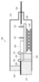
- FIG. 1 is a cross-sectional side view of a prior art HB-CDM optical transmitter.
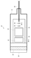
- 1 is a side cross-sectional view of an optical transmitter using HB-CDM according to an embodiment of the present disclosure.
- 1 is a side cross-sectional view of an optical transmitter using HB-CDM according to another embodiment of the present disclosure.
- 1A and 1B are diagrams for explaining limitations on the height direction of wire connection points and limitations on the spacing between a driver IC and an optical modulator chip 103 in an optical transmitter according to an embodiment of the present disclosure.
- FIG. 13 is a top view of an optical transmitter using HB-CDM according to another embodiment of the present disclosure.
- 1A and 1B are diagrams illustrating restrictions on pad positions, etc., on the circuit surface of an optical transmitter according to an embodiment of the present disclosure.
- 1A and 1B are diagrams illustrating the density arrangement of Peltier elements in an optical transmitter according to an embodiment of the present disclosure.
- This disclosure presents new configurations for improving the temperature dependency of the high-frequency characteristics of an optical transmitter in which a modulator and its driver IC are integrated into a package, and implementation forms compatible with each configuration.
- the configuration for improving the temperature dependency includes a new use of a temperature regulator (TEC: ThermoElectric Cooler) in the optical transmitter.
- TEC ThermoElectric Cooler
- various implementation forms of the driver IC, optical modulator chip, and spatial optical components compatible with the new use of the TEC are also proposed.
- TECs are also known as thermoelectric coolers, and are known as small cooling devices that use Peltier junctions. TECs are made up of n-type semiconductors, p-type semiconductors, and metals, and when a direct current is passed through both sides of the plate-shaped element, heat is absorbed on one side and dissipated on the other. Reversing the direction of the current switches between heat absorption and dissipation, allowing for localized and precise temperature control of ICs and electronic components. For simplicity's sake, in the following explanation, the temperature regulator will be referred to as a TEC and described as a Peltier element. Any device that can control the temperature of a driver IC or optical modulator chip is not limited to one that uses a Peltier element.
- FIG. 1 is a side cross-sectional view showing the implementation of an optical transmitter using HB-CDM, a conventional technology.
- the optical transmitter 100 contains a driver IC 102, an optical modulator chip 103, and lenses 112 and 113, which are spatial optical components, inside a package housing 101 made of ceramic, metal, or a combination of these. More specifically, the optical modulator chip 103 is mounted on the bottom inside the package housing 101 via a subcarrier 104 on a Peltier element 105. The right end of the optical modulator chip 103 in the drawing has an output facet for modulated light, and lenses 112 and 113 for optically coupling the modulated light to an optical fiber 114 are also mounted on the subcarrier.
- a driver IC 102 is mounted on a metal block or ceramic material 106 adjacent to the optical modulator chip 103.
- the package housing 101 has a wiring board base 107 and a package wall 108 as the left wall in the drawing, which, together with the package housing 101, separate the outside from the internal space of the optical transmitter.
- the optical transmitter 100 can also be constructed so that the entire package is airtight.
- the modulated electrical signal supplied from an external digital signal processor (DSP) is supplied to the optical modulator chip 103 via the wiring layer 109 and driver IC 102 of the wiring board base 107.
- the wiring layer 109 and the driver IC 102, and the driver IC 102 and the optical modulator chip 103 are connected by gold wires 110, 111, etc., respectively.
- the modulated electrical signal includes an I channel and a Q channel for each of the X polarization and the Y polarization.
- one channel is supplied as an electrical signal in a differential signal format, at least eight signal wirings and a GND wiring are required for one optical modulator, but the modulated signal format is not limited to this.
- the optical transmitter 100 shown in FIG. 1 can be mounted on a common device substrate together with an ICR package in which a TIA and an optical receiver on the receiving side are integrated, and a DSP, to form an optical transmitting and receiving device.
- the Peltier element 105 in the optical transmitter. Temperature control is essential for the optical modulator chip 103 fabricated on an InP substrate, and the Peltier element 105 controls the temperature to a predetermined operating temperature. As shown in FIG. 1, the Peltier element 105 has a size that covers at least the entire area of the optical modulator chip 103, and its position may overlap the area of spatial optical components such as lenses.
- the optical transmitter 100 of the conventional technology it was considered that temperature control of the driver IC 102 was not necessary, and it was fixed in the package by a member 106 such as a metal block or ceramic. If the external temperature (ambient temperature) of the optical transmitter 100 rises, the increased temperature becomes the operating temperature of the driver IC 102.
- the driver IC is also a heat source, so considering the heat generated by the driver, it is estimated that the operating temperature of the driver IC is about +5 to +10°C higher than the external temperature. If the maximum environmental temperature of the optical transmitting and receiving device including the optical transmitter is 85°C, the temperature of the driver IC 102 itself will be at least 85°C or higher. The driver IC also consumes a large amount of power, and the driver IC itself generates heat. This means that the backside temperature of the driver IC will exceed the maximum environmental temperature of 85°C due to the heat generated by the driver IC.
- the driver IC has temperature-dependent amplification characteristics (high frequency characteristics) of high frequency electrical signals, and at high temperatures the high frequency band tends to decrease compared to room temperature. Conversely, at low temperatures the high frequency band tends to increase compared to room temperature. Thus, the high frequency characteristics of the driver IC differ between low and high temperatures.
- the modulation signal supplied to the driver IC is optimized and compensated in various ways by the DSP at room temperature. However, dynamically updating such compensation in line with temperature fluctuations is a complex process and is not generally implemented. Because operation continues at a constant compensation state at room temperature, the compensation state of the modulation signal deviates from the optimal point when the state changes to a low or high temperature. This causes fluctuations and deterioration in the optical transmission characteristics and waveform quality of the optical transmitter.
- the IQ modulator of the optical modulator chip 103 is a linear modulator that preserves the amplitude and phase of the electrical signal, and fluctuations in the level and waveform quality of the modulated electrical signal directly affect the quality of the modulated output light. If the external temperature changes while the optical transmitter is in operation, the optical modulator chip itself is maintained at a constant temperature because it is temperature-controlled by a Peltier element, but the operating temperature of the driver IC changes. As a result, fluctuations in the level and quality of the HB-CDM modulated light occur, and temporal changes in the environmental temperature can cause deterioration and instability in the transmission characteristics.
- the deterioration of characteristics due to the environmental temperature on the high frequency side of the electrical signal causes waveform distortion of the modulated signal, degrading the modulation accuracy of the modulated output light from the optical modulator.
- a floor appears in the BER characteristics, leading to a deterioration in the transmission characteristics of the system.
- This disclosure presents a new configuration and implementation form that improves the temperature dependency of high frequency characteristics and optical transmission characteristics in an optical transmitter in which an optical modulator and its driver IC are packaged together.
- FIG. 2 is a side cross-sectional view showing an optical transmitter using HB-CDM according to an embodiment of the present disclosure.
- an InP optical modulator chip 13 its driver IC 12, and other components are integrated inside a package housing 11 along the HB-CDM, similar to the configuration of the conventional optical transmitter 100 shown in FIG. 1.
- the package housing 11 has a wiring board base 18 and a package wall 19 as the wall on the left side of the drawing, and the configuration for dividing the inside and outside of the package is also similar.
- the difference from the conventional configuration of FIG. 1 is the use of the TEC, i.e., the Peltier element, which performs temperature control.
- the driver IC 12 is also mounted on the same Peltier element 16 as the optical modulator chip 13 and the lenses 23 and 24, which are optical mounting members. This makes it possible to control the temperature of the driver IC as well.
- the driver IC 12, optical modulator chip 13, and lenses 23 and 24 are mounted on the Peltier element 16 via the subcarrier 14.
- the subcarrier 14 functions as a base for fixing and holding the driver IC, optical modulator chip, and spatial optical components.
- the subcarrier 14 has wiring for connecting to the DC wiring of the optical modulator chip, RF lines for connecting the driver IC and optical modulator chip, and even positioning markers for mounting the spatial optical components, formed by metal patterns 15.
- the material of the subcarrier 14 is preferably one with excellent thermal conductivity, since it will be equipped with the driver IC 12 and optical modulator chip 13, which are the targets of temperature control.
- a ceramic substrate such as an AlN substrate is preferable.
- the material constant of the AlN substrate is close to that of InP, so it is also compatible with the InP optical modulator in terms of behavior with respect to temperature changes.
- the ceramic on the upper surface of the Peltier element 16 is made of AlN.
- a metal with excellent thermal conductivity, such as CuW, may be used as the material of the subcarrier 14.
- a wiring board is placed on at least a part of the upper surface of the subcarrier as an alternative to the metal pattern 15 on which the above-mentioned RF lines and positioning markers are formed, and the RF lines and positioning markers are formed on the wiring board.
- the Peltier element 16 and the subcarrier 14 are joined with an adhesive or the like that has low thermal resistance and high thermal conductivity. Specifically, it is desirable to mount the subcarrier 14 on the top surface of the Peltier element 16 using a paste or solder with excellent thermal conductivity of 30 W/(mK) or more.
- the subcarrier 14 is depicted as being made of a single layer of AlN, but it can also be a multi-layer AlN substrate.
- a multi-layer substrate By using a multi-layer substrate, it is possible to implement a flexible element and wiring layout that makes full use of multi-layer wiring when there are a large number of DC wirings to the optical modulator or when cross wiring is required to change the order of the terminals. From the perspective of RF design, multi-layer wiring also makes it possible to provide a GNG on the back side of the wiring, which increases the freedom of the wiring layout, such as narrowing the width of each wiring or wiring at a high density, and is extremely effective.
- the driver IC 12 and the optical modulator chip 13 are flip-chip mounted face-down using pillars or bumps, or a combination of these with solder.
- the driver IC 12 and the optical modulator chip 13 are placed on a metal pattern 15 formed on the surface of the subcarrier 14, with the circuit surface (face) on which the electrode pads are formed of the main surface facing the bottom surface of the package housing 11 (i.e., with the surface on which the electrode pads are formed facing downwards).
- the pillars can be, for example, Au pillars or Cu pillars.
- the gap between the driver IC 12 and the optical modulator chip 13 mounted face-down by flip-chip mounting and the subcarrier 14, which is equivalent to the height of the Au pillar or bump, is filled with an underfill material 17 with excellent thermal conductivity.
- an underfill material with a thermal conductivity of 3 W/(mK) or more.
- the underfill material is a dielectric material and has a certain dielectric constant and dielectric tangent, which may lead to loss in high-frequency wiring such as the optical modulator. Please note that depending on the high-frequency band and baud rate required for the optical modulator, it is possible to prioritize high-frequency characteristics over temperature stability and bond strength and not use the underfill material.
- the driver IC is a heating element and was not considered to be a target for temperature control by a Peltier element. Driving power is required to operate the Peltier element, and no consideration was given to using extra power for a heating element.
- the inventors came up with the new idea of adding temperature control to the heating element.
- the optical transmitter 10 disclosed herein is capable of simultaneously controlling the temperature of the optical modulator chip 13 and the driver IC 12 using a single Peltier element 16. Although not shown in FIG. 2, the Peltier element 16 is connected to a control current source. As for the specific control temperatures of each part, it is generally desirable to use an InP optical modulator at around 45 ⁇ 10°C, since the modulation efficiency decreases if the temperature is too low.
- the Peltier element 16 only needs to be controlled at any temperature between 25°C and 50°C, which is a temperature at which the characteristics of the InP optical modulator in the optical modulator chip 13 do not deteriorate significantly and the characteristics of the driver IC can be fully brought out.
- All spatial optical components such as lenses 23 and 24 for optically coupling modulated light with optical fiber 25 are mounted on the Peltier element 16 to suppress the thickness variation of the adhesive caused by temperature changes. This makes it possible to minimize the variation of the optical insertion loss caused by the optical axis shifting due to temperature changes.
- the spatial optical components also include a member for fixing the fiber and a polarization beam combiner (PBC). In order to align the position of the lenses 23 and 24 with the optical axis of the light output from the optical modulator chip 13 flip-chip mounted face-down, the portion of the subcarrier 14 on which the optical components are mounted is made thin.
- FIG. 3 shows a modified form of the optical transmitter 10, which is configured with a subcarrier 14-1 carrying the optical modulator chip 13 and the driver IC 12, and a subcarrier 14-2 carrying the lenses 23 and 24.
- the subcarrier 14-2 may be omitted, and the lenses 23 and 24 may be mounted directly on a TEC such as a Peltier element 16.
- an optical transmitter 10 in HB-CDM form is shown as an example, but similar effects can be obtained with other package forms as long as the optical transmission module is an integrated configuration of a driver IC and optical modulator.
- an example is shown in which wiring from a DSP that supplies a modulation signal to the driver IC 12 is connected by a flexible printed circuit board (FPC) on an RF terrace. That is, the metal pattern 20 formed on the wiring layer on the top surface of the wiring board base 18 on the outside of the optical transmitter is connected to an FPC cable (not shown).
- FPC flexible printed circuit board
- the FPC interface has superior high-frequency characteristics because it does not require RF vias (VIAs), etc.
- the electrode pads of the driver IC 12 and the electrode pads of the optical modulator chip 13 are connected by high-frequency wiring of the metal pattern 15 of the subcarrier 14 made of an AlN substrate by flip-chip mounting using pillars or bumps, or a combination of them and solder.
- flip-chip mounting is difficult between the electrode pads of the driver IC 12 and the electrode pads of the metal pattern 20 on the RF terrace, they are connected by wire lines 21.
- the inductance between the driver IC 12 and the optical modulator chip 13 is what contributes most to the high-frequency characteristics. For example, if the wire is long, the series inductance component increases, and the roll-off frequency in the high-frequency characteristics shifts to the low-frequency side due to LC resonance. Therefore, in order to expand the high-frequency characteristics of the driver IC and improve the quality of the modulated high output, it is desirable for the inductance of the wire to be low.
- the driver IC 12 and the optical modulator chip 13 are connected by flip-chip mounting.
- the inductance of the wire connection between the electrode pad of the driver IC 12 and the electrode pad of the metal pattern 20 on the RF terrace has a small effect on the high-frequency characteristics, it is desirable for the inductance to be as small as possible. Therefore, regulations are established regarding the height and planar directions of the wire connection part.
- Figure 4 is a diagram explaining the height restriction of the wire connection point in the optical transmitter 10 and the restriction of the distance between the driver IC and the optical modulator chip 103.
- the electrodes of the metal pattern 20 of the RF terrace, the driver IC 12, and the vicinity of the upper surface of the optical modulator chip 13 are shown enlarged in the height direction.
- the inductance between the electrodes of the metal pattern of the RF terrace and the electrodes of the driver IC has a smaller effect on the characteristics than the inductance between the electrodes of the driver IC and the electrodes of the optical modulator, it is desirable to make it as small as possible.
- the difference in height between the upper surface of the electrode of the RF terrace connected by the wire line 21 and the upper surface of the metal pattern 15 of the subcarrier 14 100 ⁇ m or less.
- This restriction is the minimum range that can be realized, taking into account the variation in thickness of the driver IC and the variation in the mounting materials of the subcarrier 14.
- the height of the Peltier element 16 may be changed, the thickness of the subcarrier 14 may be changed, or the height of the RF terrace of the wiring board base 18 made of ceramic may be changed.
- the difference in height between the upper surface of the electrode of the RF terrace and the upper surface of the metal pattern 15 of the subcarrier 14 is not necessarily required.
- the upper surface of the electrode of the RF terrace and the upper surface of the metal pattern 15 of the subcarrier 14 may be configured to be at the same height.
- the longer the wiring length the greater the wiring loss and the more the high frequency characteristics deteriorate. It is desirable to make the distance between the driver IC 12 and the optical modulator chip 13 short. However, if the driver IC 12 and the optical modulator chip 13 are too close, the temperature control of the driver IC 12 and the optical modulator chip 13 by one Peltier element 16 may not work sufficiently, or the heat of the driver IC may be transferred to the optical modulator chip, which may cause the operation of the optical transmitter 10 to become unstable. Therefore, it is desirable to separate the driver IC 12 and the optical modulator chip 13 by at least 500 ⁇ m.
- the distance between the driver IC 12 and the optical modulator chip 13 5 mm or less.
- the length of the RF wiring connecting the electrode pads of the optical modulator chip 13 and the electrode pads of the driver IC 12 is 500 ⁇ m or more and 5 mm or less.
- FIG. 5 is a top view showing a modified embodiment of the mounting form of the optical transmitter of the present invention. It corresponds to a top view of the circuit surface inside the module, with the package housing 11 of the optical transmitter 10 shown in FIG. 2 cut away.
- grooves 30-1 and 30-2 are formed on the top surface of the subcarrier 14, as shown by the dotted lines.
- the high-frequency wiring of the subcarrier 14 is configured in an area 33 shown by the dotted line between the driver IC 12 and the optical modulator chip 13.
- the driver IC 12 and the optical modulator chip 13 have electrode pads for RF connection formed around them.
- a linear groove 30-2 is formed only on one side of the high-frequency wiring region 33 for the driver IC 12, and a rectangular groove 30-1 is formed near the periphery 4 of the optical modulator chip 13.
- the shape of the groove is not limited to the configuration shown in FIG. 5, and can be changed according to the properties of the underfill material 17 and the shape of the wiring on the subcarrier 14 that should be avoided.
- the groove 30-2 on the driver IC 12 side is only on one side on the optical modulator chip 13 side, but it may be formed in a rectangular shape at a position corresponding to the periphery 4 of the driver IC.
- FIG. 5 In addition to the configuration of FIG.
- a linear groove may be added to the position on the RF terrace side of the driver IC 12, that is, on one side on the wiring board base 18 side. Furthermore, in FIG. 5, a rectangular groove 30-1 is formed at a position corresponding to the periphery 4 of the optical modulator chip 13, but the groove may be formed only at a position corresponding to two sides on the driver IC 12 side and the lenses 23 and 24 side described below.
- the linear groove 30-2 on the driver IC 12 side and the rectangular groove 30-1 on the optical modulator chip 13 side, that on the driver IC side, also serve as a thermal isolation groove between the optical modulator chip and the driver IC. That is, a groove can be provided on the surface of the subcarrier 14 near at least one of the opposing sides of the driver IC 12 and the optical modulator chip 13. If the subcarrier 14 is composed of a multilayer board, high-frequency wiring can be formed on the inner layer, so a groove can also be formed in the region 33. By forming a groove on at least one of the upper or lower surfaces of the subcarrier 14 between the driver IC 12 and the optical modulator chip 13, this groove can also serve as a thermal isolation groove.
- the underfill material rises up near the chip end face on the lens side of the optical modulator chip 13, the underfill material may adhere to the emission end face and deteriorate the optical coupling with the lenses 23 and 24.
- the groove on one side of the rectangular groove 30-1 on the optical modulator chip 13 side on the lens 23 side shown in FIG. 45 is also effective in avoiding such optical coupling problems.
- the subcarrier 14 is formed in a multi-layer structure, it is possible to avoid the effects of the above-mentioned underfill material by configuring the high-frequency line as an inner layer of the subcarrier. Also, if the high-frequency wiring is configured as an inner layer, a groove can be formed at any location on the top surface of the subcarrier between the optical modulator chip and the driver IC. It goes without saying that sufficient consideration must be given to the effects on disconnection of the inner layer wiring and characteristic impedance. On the other hand, when designing high-frequency wiring with the same line impedance, the signal line width becomes narrower in the inner layer wiring due to the influence of the effective dielectric constant of the subcarrier. Furthermore, since it is also affected by the dielectric loss tangent of the subcarrier, it is desirable to have the wiring pattern on the outermost surface of the subcarrier 14 when only considering the loss of the high-frequency line.
- the lenses 23 and 24 are arranged on the opposite side of the optical modulator chip 13 from the driver IC 12.
- at least one lens may be arranged on the upper or lower side of the optical modulator chip 13 when viewed from the top view of FIG. 5.
- the PBC may be arranged on a side different from the driver IC 12 of the optical modulator chip 13.
- the spatial optical components are mounted above the Peltier element 16 on a side different from the side of the optical modulator chip 13 facing the driver IC 12.
- a groove for allowing excess underfill material to escape may be formed near the side of the optical modulator chip that corresponds to the spatial optical components.
- Figure 6 is a diagram explaining the limitations of pads etc. on the circuit surface of an optical transmitter, as viewed from the subcarrier 14 side.
- Figure 6 shows an electrode pad 26 on the output side of the driver IC 12 and an electrode pad 27 on the input side of the optical modulator chip 13.
- pillars and solder 30 and 31 for flip-chip connection with the metal pattern 15 formed on the surface of the subcarrier 14 are formed on the electrode pads 26 and 27, respectively.
- the electrode pad 26 on the output side of the driver IC 12 is configured as GSGSG
- the electrode pad 27 on the input side of the optical modulator chip 13 is configured as GSSG.
- differential driving is more preferable than single-ended driving
- the optical modulator chip 13 is also differentially driven due to the connectivity with the driver IC 12 that drives differentially.
- a differential line such as a GSGSG or GSSG configuration is also laid out as RF wiring in the metal pattern 15 formed on the surface of the subcarrier 14. If the differential line includes a bent portion, the characteristics tend to deteriorate. Therefore, in this embodiment, as shown in FIG.
- the position of the electrode pad 26 on the output side of the driver IC 12 and the position and channel pitch of the electrode pad 27 on the input side of the optical modulator chip 13 are not significantly shifted so that the RF wiring, i.e., the differential line, is formed in a straight line.
- the differential line is shown by a dashed line.
- the metal pattern 15 may be provided with differential lines that include bends or taper shapes that do not significantly degrade the characteristics of the differential lines.
- lenses 23 and 24 are implemented as spatial optical components, but this also includes fiber fixing members, PBC, etc.
- FIG. 7 is a diagram illustrating the density arrangement of Peltier elements in an optical transmitter according to one embodiment of the present disclosure.
- the Peltier element 16 has a large number of n-type and p-type semiconductor elements arranged between the upper and lower metal surfaces, and realizes the movement of heat between the two surfaces as a whole. Therefore, the arrangement density of the semiconductor elements in the Peltier element can be set according to the amount of heat generated by the object to be temperature controlled. Considering the amount of heat generated by each part in the optical transmitter, the driver IC generates the most heat, followed by the optical modulator chip and the spatial optical components. Specifically, the element density of the Peltier elements is set so that the mounting area of the driver IC > the mounting area of the optical modulator chip > the mounting area of the spatial optical components.
- the area 16-1 of the Peltier element that controls the driver IC 12 should have the highest element density.
- the area 16-2 of the Peltier element that controls the optical modulator chip 13 should have a medium element density, and the area 16-3 where the spatial optical components including the lenses 23 and 24 are arranged should have a low element density.
- this disclosure makes it possible to suppress the temperature dependency of optical modulation output characteristics and realize a new configuration and implementation form of an optical transmitter with excellent high speed performance.
- This disclosure provides an optical transmitter with improved temperature dependency of optical modulation output characteristics that can be used in optical communication networks.
Landscapes
- Physics & Mathematics (AREA)
- Nonlinear Science (AREA)
- General Physics & Mathematics (AREA)
- Optics & Photonics (AREA)
- Optical Modulation, Optical Deflection, Nonlinear Optics, Optical Demodulation, Optical Logic Elements (AREA)
Abstract
光送信器(10)は、ペルチェ素子(16)と、光変調器(13)と、光変調器のための変調電気信号を供給するドライバ集積回路(IC)(12)と、を備え、光変調器およびドライバICは、ペルチェ素子の上面に対してフェイスダウンで、フリップチップ実装される。光変調器を含む光変調器チップおよびドライバICは、ペルチェ素子の上面に配置されたサブキャリア(14)の上面にフリップチップ実装される。サブキャリアは窒化アルミニウム(AlN)を用いて形成され、光変調器チップはInPを用いて形成され、サブキャリアと光変調器チップおよびドライバICと間の隙間に3W/(mK)以上の熱伝導率を有するアンダーフィル材(17)が充填される。ペルチェ素子の温度は25℃以上50℃以下で制御される。
Description
本開示は、光通信において利用される光送信器に関する。より詳細には、半導体光変調器およびそのドライバICを含む光送信器の実装形態に関する。
通信ネットワークの急激なトラフィック増大に応えるため、コヒーレント通信方式とデジタル信号処理技術を組み合わせたデジタルコヒーレント光伝送が光ファイバ通信システムに導入されている。当初の1波長当たり100Gbpsの基幹網伝送技術の確立から始まり、現在ではより高速化された1波長当たり400~600Gbpsの伝送が実用化されている。
上述のデジタルコヒーレント光伝送では、光受信器および光送信器を集積化した光送受信装置が利用されている。伝送容量が400Gbpsを超えるシステムの光送受信装置では、高周波(RF)電気回路などのアナログ部品の広帯域化が求められており、例えば光変調器では40GHz以上の変調帯域が必要である。広帯域化につながる高周波損失の低減や装置の小型化のため、例えば送信側ではRFドライバICおよび光変調器が一体パッケージに実装された形態が注目されている。この光送信器の実装形態は,High-Bandwidth Coherent Driver Modulator (HB-CDM:高速ドライバ集積光変調器)という名前でOIF(The Optical Internetworking Forum)で標準化もされている(非特許文献1)。光送受信装置の受信側でも、トランスインピーダンスアンプ(TIA)および光受光器が一体パッケージに実装され、ICR(Integrated Coherent Receiver)とも呼ばれている。
光送受信デバイスの材料に目を転じると、小型・低コスト化の観点で、従来のニオブ酸リチウム(LN)光変調器に代わって、半導体ベースの光変調器が注目を集めている。より高速な変調動作向けには、InPに代表される化合物半導体が主に用いられている。また、より小型・低コスト化が重要視されるシステムにおいては、Siベースの光デバイスに研究開発が集中している。
上述の半導体による光変調器においても材料固有の得失があり、例えばInP光変調器においては、バンド端吸収効果を制御するために、動作時には光変調器チップの温度制御が必須である。一方、Si光変調器は温度制御が不要となるメリットがあるものの、他の材料系と比べて電気光学効果が小さい。このため電気-光相互作用長を長くする必要が生じ、デバイス長が大きくなる結果として高周波損失増大を招くことがある。広帯域化および小型化のための実装技術を含めて、光変調器のさらなる高速化・広帯域化には課題が多い。
HB-CDMによる光送信器の動作温度(ケース温度)としては、少なくとも-5℃~75℃の範囲が求められている。このような動作温度を確保するため、消費電力も考慮して光変調器チップのみがペルチェ素子上に実装されているのが一般的であった(特許文献1)。
OIF, Implementation Agreement for the High Bandwidth Coherent Driver Modulator (HB-CDM), [online], July 15,2021, [令和 4年9月1日検索],インターネット<URL: https://www.oiforum.com/wp-content/uploads/OIF-HB-CDM-02.0.pdf>
J. Ozaki et al., "500-Gb/s/λ Operation of Ultra-Low Power and Low-Temperature-Dependence InP-Based High-Bandwidth Coherent Driver Modulator," in Journal of Lightwave Technology, vol. 38, no. 18, pp. 5086-5091, 15 Sept.15, 2020, doi: 10.1109/JLT.2020.2998466.
しかしながら、従来技術の光送信器では、高温時におけるドライバICの高周波特性の劣化が問題となっていた。具体的には環境温度が高温状態にある場合に、ドライバICの高周波帯域、ピーキング量やゲインが劣化することが問題となっていた。光送信器が高速化・広帯域化する中で、上述の劣化による信号品質の低下の影響が無視できなくなってきた。そのため、環境温度の変化に関わらず、一定の高周波特性を維持することのできる光送信器が望まれている。
本開示は、上述の課題に鑑み、ドライバICを含む光送信器の温度依存性を抑え、高速性に優れ、環境温度によらず安定動作が可能な光送信器の新規な構成および実装形態を提供する。
本開示の1つの態様は、光送信器であって、ペルチェ素子と、光変調器と、光変調器のための変調電気信号を供給するドライバ集積回路(IC)と、を備え、光変調器およびドライバICが、ペルチェ素子の上面に対してフェイスダウンで、フリップチップ実装された光送信器である。
本開示により、ドライバICを含む光送信器の温度依存性を抑え、高速性に優れ、環境温度によらず安定動作が可能な光送信器の新規な構成および実装形態を実現できる。
本開示は、変調器とそのドライバICが一体にパッケージ実装された光送信器において、光送信器の高周波特性の温度依存性改善のための新しい構成と、各構成に適合する実装形態を提示する。温度依存性を改善する構成は、光送信器における温度調整器(TEC:ThermoElectric Cooler)の新しい利用形態を含む。さらに、TECの新しい利用形態に適合した、ドライバIC、光変調器チップおよび空間光学部品の様々な実装形態も提案する。
TECは熱電クーラーとも呼ばれ、ペルチェ接合による小型冷却デバイスとして知られている。TECは、n型半導体、p型半導体および金属から構成されており、板状に形成された素子の両面に直流電流を流すと、一方の面で吸熱、もう一方の面で放熱が起こる。電流の向きを逆にすれば吸熱と放熱が切り替わるので、ICや電子部品の局所的で正確な温度コントロールが可能である。以下の説明では、簡単のため温度調整器をTECと呼び、ペルチェ素子として説明する。ドライバICや光変調器チップの温度制御が可能なものであれば、ペルチェ素子によるものに限定されない。
以下では、従来技術のHB-CDMの形態による光変調器を例として、光送信器における高周波特性の温度依存性の問題を最初に説明する。その後、本開示の光送信器による、高周波特性の温度依存性を改善する新規な構成について、様々な実装形態とともに説明する。
図1は、従来技術のHB-CDMによる光送信器の実装形態を示す側断面図である。光送信器100は、HB-CDMの仕様に沿って、セラミック、金属等またはこれらの組み合わせによるパッケージ筐体101の内部にドライバIC102、光変調器チップ103、空間光学部品であるレンズ112、113などが収納されている。より具体的には、パッケージ筐体101の内部の底面には、ペルチェ素子105の上のサブキャリア104を介して光変調器チップ103が搭載されている。光変調器チップ103の図面上で右端には変調光の出射端面があり、変調光を光ファイバ114と光結合するためのレンズ112、113もサブキャリア上に搭載されている。
光変調器チップ103に隣接して、金属ブロックやセラミック材106上にドライバIC102が搭載されている。さらに、パッケージ筐体101の図面上の左側の壁面として、配線基板ベース107およびパッケージ壁面108を備えており、パッケージ筐体101とともに、外部と光送信器の内部空間を区画する。光送信器100は、パッケージ全体が気密性を確保して構成されることもできる。
外部のデジタル信号プロセッサ(DSP)から供給される変調電気信号は、配線基板ベース107の配線層109、ドライバIC102を経て、光変調器チップ103へ供給される。配線層109およびドライバIC102の間、ドライバIC102および光変調器チップ103の間は、金のワイヤ線110、111等でそれぞれ接続されている。変調電気信号は、偏波多重型IQ光変調方式の場合、X偏波およびY偏波のそれぞれについて、IチャネルおよびQチャネルを含む。1つのチャネルが差動信号形式の電気信号として供給される場合、1つの光変調器に対して少なくとも8本の信号配線、さらにGND配線が必要となるが、変調信号形式はこれに限定されない。図1に示した光送信器100は、特許文献1に示されているように、受信側のTIAおよび光受光器が一体に集積されたICRパッケージやDSPとともに、共通の装置基板に搭載されて、光送受信装置を構成できる。
ここで再び、光送信器内のペルチェ素子105に着目する。InP基板に作製された光変調器チップ103では温度制御が必須であり、ペルチェ素子105によって所定の動作温度にコントロールされている。図1に示したように、ペルチェ素子105は、少なくとも光変調器チップ103の全体領域をカバーするようなサイズを持ち、その位置がレンズなどの空間光学部品の領域に掛る場合もある。一方で、従来技術の光送信器100では、ドライバIC102の温度制御は必要が無いと考えられており、金属ブロックやセラミックなどの部材106によってパッケージ内に固定されていた。光送信器100の外部温度(環境温度)が上昇すれば、その上昇した温度がドライバIC102の動作温度となる。実際にはドライバICも発熱体であるため、ドライバからの発熱を考慮すると、ドライバICの動作温度は、外部温度に対して+5~10℃くらい高い温度になっていると見積もられる。光送信器を含む光送受信装置が使用される最大環境温度の85℃の状態になれば、ドライバIC102自体の温度も少なくとも85℃以上となっていた。ドライバICも大きな消費電力を持っており、ドライバIC自体が発熱することになる。したがって、ドライバICの発熱の影響により、ドライバICのバックサイド温度は、最大環境温度の85℃を超えることを意味している。
ドライバICは、高周波電気信号の増幅特性(高周波特性)に温度依存性を持っており、高温状態では、室温状態と比較して高周波帯域が低下する傾向にある。逆に低温状態では、室温状態と比較して高周波帯域は増大する傾向にある。このように、低温状態と高温状態の間で、ドライバICの高周波特性が異なる。ドライバICに供給される変調信号は、室温状態においてDSPによって様々な最適化や補償が行われている。しかしながら、このような補償を温度変動とともに動的に更新しながら行うのは複雑な処理であり、一般には実施されていない。常温時における一定の補償状態のままで動作を続けるため、低温状態や高温状態に変わった際には、変調信号の補償状態は最適点からずれることになる。このため、光送信器の光伝送特性および波形品質に変動や劣化が生じていた。
光変調器チップ103のIQ変調器は電気信号の振幅・位相を保存する線形変調器であり、変調電気信号のレベルや波形品質の変動は、変調出力光の品質に直接的な影響を与える。光送信器の動作中に外部温度が変わると、光変調器チップ自体はペルチェ素子で温度管理されているため一定温度に維持されるが、ドライバICの動作温度は変化してしまう。結果として、HB-CDMの変調光のレベル変動や品質変動が生じ、環境温度の時間的な変化によって、伝送特性が劣化し、安定しない問題も生じる。
電気信号の高域側での環境温度に起因した特性劣化は、変調信号の波形歪みを生じ、光変調器からの変調出力光の変調精度が劣化する。このような劣化した変調光を受信する光受信器では、BER特性にフロアが生じるなど、システムの伝送特性の低下にも繋がっていた。
変調電気信号の広帯域化の要請が進み、40GHz以上の変調帯域が求められる状況の下で、上述のような高温時における、ドライバICの高周波特性が劣化する影響は無視できない。本開示は、光変調器とそのドライバICが一体にパッケージ実装された光送信器において、高周波特性および光伝送特性における温度依存性を改善する新しい構成および実装形態を提示する。
図2は、本開示の一実施形態に係るHB-CDMによる光送信器を示す側断面図である。本実施形態の光送信器10は、図1に示した従来技術の光送信器100の構成と同様に、HB-CDMに沿ったパッケージ筐体11の内部にInPによる光変調器チップ13およびそのドライバIC12他が一体に構成されている。パッケージ筐体11の図面上左側の壁面として、配線基板ベース18およびパッケージ壁面19を備え、パッケージの内外を区画する構成も同様である。図1の従来技術の構成との相違点は、温度制御を行うTEC、すなわちペルチェ素子の利用形態にある。図1の光送信器100におけるペルチェ素子の利用形態とは異なり、ドライバIC12も光変調器チップ13および光学実装部材であるレンズ23および24と同一のペルチェ素子16の上に実装されている。これにより、ドライバICついても温度制御が可能となっている。
ペルチェ素子16の上には、サブキャリア14を介してドライバIC12、光変調器チップ13およびレンズ23、24が実装されている。サブキャリア14は、ドライバIC、光変調器チップおよび空間光学部品を固定し保持する土台として機能する。また、サブキャリア14には光変調器チップのDC配線と接続するための配線や、ドライバICと光変調器チップとを接続するためのRF線路、更には、空間光学部品を搭載するための位置出しマーカー等がメタルパターン15によって形成されている。
サブキャリア14の材料としては、温度制御の対象であるドライバIC12および光変調器チップ13を搭載するので熱伝導率が優れている方が望ましい。具体的には、AlN基板等のセラミック基板が好ましい。AlN基板はInPとの材料定数が近いため、温度変化に対する挙動の点でもInPによる光変調器との相性も良い。同様の理由および材料の一致性という観点からも、ペルチェ素子16の上面のセラミックもAlNから構成されていることが望ましい。CuW等の熱伝導率が優れている金属をサブキャリア14の材料としてもよい。サブキャリアの材料として金属を用いる場合は、上述したRF線路および位置出しマーカー等が形成されたメタルパターン15の代替として、サブキャリアの上面の少なくとも一部分に配線基板を配置し、当該配線基板にRF線路および位置出しマーカーを形成することになる。
ペルチェ素子16とサブキャリア14とは、ペルチェ素子での熱引きの観点から、熱抵抗の小さく熱伝導率の高い接着剤等により接合されていることが望ましい。具体的には、熱伝導率が30W/(mK)以上の熱伝導性に優れたペーストまたははんだによりを用いてサブキャリア14をペルチェ素子16の上面に実装することが望ましい。
図2では、サブキャリア14は1層構造のAlNで構成されているように描かれているが、多層のAlN基板とすることもできる。多層基板を利用することで、光変調器へのDC配線数が多い場合や、端子の順番入れ替えのためにクロス配線を行う必要がある場合に、多層配線を駆使した柔軟な素子・配線レイアウトを行うことが可能である。RF設計の観点からも、多層配線とすることで配線の裏面側にGNGを設けることが可能となり、1本の配線の幅を狭くすることや高密度に配線すること等、配線のレイアウトの自由度が増え、非常に有効である。
ドライバIC12および光変調器チップ13は、ピラーまたはバンプを用いた、若しくはそれらとはんだの組み合わせを用いたフェイスダウンでのフリップチップ実装されている。ドライバIC12および光変調器チップ13は、主面のうちの電極PAD形成された回路面(フェイス)をパッケージ筐体11の底面に向けて(すなわち、電極PAD形成された面を下向きにして)、サブキャリア14の表面に形成されたメタルパターン15上に配置されている。ピラーは、たとえばAuピラーまたはCuピラー等を用いることができる。
ドライバIC12、光変調器チップ13、レンズ23、24が傾かないようにフリップチップ実装するためは、サブキャリア14の搭載面の平面度を管理することが非常に重要である。たとえば、サブキャリア14の搭載面の平面度を0.05mm以下とすることにより、安定したフリップチップ実装を実現することができる。
フェイスダウンでフリップチップ実装されたドライバIC12および光変調器チップ13とサブキャリア14との間のAuピラーまたはバンプの高さ相当の隙間には、熱伝導性に優れたアンダーフィル材17が充填されている。たとえば、3W/(mK)以上の熱伝導率を有するアンダーフィル材を用いることが望ましい。このようにして、フェイスダウンでフリップチップ実装されたドライバIC12および光変調器チップ13の接合強度を増すとともに温度制御を効果的に行うことができる。アンダーフィル材については、これを省略する構成も可能である。アンダーフィル材は誘電体であり、一定の誘電率および誘電正接を有するため、光変調器等の高周波配線の損失につながるおそれもある。光変調器に求められる高周波帯域、ボーレートによっては、温度安定性や接合強度よりも高周波特性をより優先して、アンダーフィル材を使用しない構成もあり得ることに留意されたい。
前述のように、ドライバICは発熱体であってペルチェ素子によって温度制御すべき対象とは考えられてはいなかった。ペルチェ素子を動作させるためには駆動電力が必要であって、発熱体のためにわざわざ余計な電力を使用することは考慮されなかった。しかしながら、光送信器の広帯域化の実現のために、発明者らは発熱体に対して温度制御を加えると言う新しい着想に至った。
本開示の光送信器10は、1つのペルチェ素子16により、光変調器チップ13およびドライバIC12を同時に温度制御することが可能となっている。図2には明示されていないが、ペルチェ素子16は、制御電流源に接続されている。各部の具体的な制御温度については、InP光変調器は温度が低すぎると変調効率が低下するため、一般的に45±10℃程度で使用されることが望ましい。
一方、ドライバIC12については、高温状態よりも低温状態の方が高周波特性の良いことが知られている。そのため、光変調器チップ13におけるInP光変調器の特性の劣化が大きくなく、かつドライバICの特性を十分に引き出せる温度として、ペルチェ素子16は、25℃以上50℃以下の任意の温度で制御されていればよい。
変調光を光ファイバ25と光結合するためのレンズ23、24などの空間光学部品についても、温度変化による接着剤の厚み変動等を抑えるために、全てをペルチェ素子16の上に実装するようにした。これにより温度変化によって光軸がずれることによる光挿入損失の変動等を最小化することができる。尚、空間光学部品としては、ファイバ固定用の部材や、偏波ビームコンバイナ(Polarization Beam Combine:PBC)等も含まれる。フェイスダウンでフリップチップ実装された光変調器チップ13から出力される光の光軸に、レンズ23、24の位置を合わせるために、サブキャリア14の光学部品を搭載する部分を薄くしている。レンズ23、24の径が小さい場合など、位置を合わせのための段差が不要な場合には、厚みが一定のサブキャリア14を用いてもよい。図2は、1つのサブキャリア14に厚みのことなる2つの部分を設ける例を示すが、2つの部分を分離した構成としてもよい。図3は光送信器10の変形形態を示す図であり、光変調器チップ13およびドライバIC12を搭載するサブキャリア14-1と、レンズ23、24を搭載するサブキャリア14-2とを備えた構成である。サブキャリア14-2を省略して、レンズ23、24をペルチェ素子16のようなTECの上に直接搭載する構成としてもよい。
図2では、一例としてHB-CDM形態の光送信器10を示しているが、ドライバICと光変調器が一体に構成されている光送信モジュールであれば、他のパッケージ形態であっても、同様の効果が得られる。また図2では、ドライバIC12へ変調信号を供給するDSPからの配線を、RFテラス上でフレキスブル配線板(FPC)により接続される例を示している。すなわち、光送信器の外側の配線基板ベース18の上面の配線層に形成された金属パターン20において、図示しないFPCケーブルと接続される。FPCインタフェースは、表面実装技術(SMT)を利用した構成と比べ、RFビア(VIA)等が不要であるため高周波特性に優れている。
次に、ドライバIC12の高周波特性および光変調器の変調高出力の品質の改善に寄与する実装構造について述べる。図2に示した様に、本実施形態のHB-CDM形態の光送信器10において、ドライバIC12の電極パッドと光変調器チップ13の電極パッドとは、ピラーまたはバンプを用いた、若しくはそれらとはんだの組み合わせを用いたフリップチップ実装により、AlN基板で構成されたサブキャリア14のメタルパターン15の高周波配線にて接続される。一方、ドライバIC12の電極パッドとRFテラス上の金属パターン20の電極パッド間はフリップチップ実装が困難であるため、ワイヤ線21にて接続される。高周波特性に最も寄与するのは、ドライバIC12と光変調器チップ13との間のインダクタンスである。たとえば、ワイヤが長いと直列インダクタンス成分が増えることにより、LC共振に起因して高周波特性におけるロールオフ周波数が低域側にシフトしてきてしまう。したがって、ドライバICにおける高周波特性を拡大し、変調高出力の品質を向上するためには、ワイヤのインダクタンスは低いことが望ましい。この点において、本実施形態では、ドライバIC12と光変調器チップ13との間をフリップチップ実装により接続している。これにより、図1の光送信器100のようなワイヤにより接続に比べて、ドライバIC12と光変調器チップ13との間のインダクタンスを約10分の1から5分の1程度まで下げることができ、広帯域化を可能としている。
ドライバIC12の電極パッドとRFテラス上の金属パターン20の電極パッド間のワイヤ接続のインダクタンスが高周波特性に与える影響は小さいものの、インダクタンスはなるべく小さいほど望ましい。そこで、ワイヤ接続する部分の高さ方向および平面方向についての規定を設けている。
図4は、光送信器10におけるワイヤ接続箇所の高さ方向の制限およびドライバICと光変調器チップ103との間隔の制限を説明する図である。図2において、RFテラスの金属パターン20の電極、ドライバIC12および光変調器チップ13の上面の近傍を高さ方向に拡大して示している。RFテラスの金属パターンの電極とドライバICの電極との間のインダクタンスは、ドライバICの電極と光変調器の電極との間のインダクタンスに比べて、特性に与える影響は小さいものの、できるだけ小さいことが望ましい。図4に示したように、ワイヤ線21によって接続されるRFテラスの電極の上面とサブキャリア14のメタルパターン15の上面との高さの差は、100μm以下とすることが望ましい。この制限は、ドライバICの厚みばらつきやサブキャリア14の実装部材のばらつきを考慮して、実現可能な最小な範囲である。たとえば、ペルチェ素子16の高さを変えてもよいし、サブキャリア14の厚みを変えてもよいし、またはセラミックで構成された配線基板ベース18のRFテラスの高さを変えてもよい。同様に、配線基板ベース18のRFテラスの電極パッドとドライバパッケージ(不図示)の電極パッドとの間のギャップも100μm以下とすることが望ましい。なお、RFテラスの金属パターンの電極とドライバICの電極との間をリボンボンディング等により接続する場合には、RFテラスの電極の上面とサブキャリア14のメタルパターン15の上面との高さの差は必ずしも必要ではない。すなわち、RFテラスの電極の上面とサブキャリア14のメタルパターン15の上面との高さが等しくなるように構成してもよい。
また高周波特性の観点から考えると、配線長が長いほど配線損失が増えて高周波特性が劣化する。ドライバIC12と光変調器チップ13と間の距離を近くすることが望ましい。しかし、ドライバIC12と光変調器チップ13とが近すぎると、1つのペルチェ素子16によるドライバIC12および光変調器チップ13に対する温度制御が十分に作用しないことやドライバICの熱が光変調器チップに伝わることにより、光送信器10の動作が不安定になる虞がある。よって、ドライバIC12と光変調器チップ13との間は、少なくとも500μm以上離すことが望ましい。500μm以上離すことで、実装時のジグ等のアクセスも容易になるので、製造の観点でも適切であると言える。ただし、高周波特性を考えると、ドライバIC12と光変調器チップ13と間の距離が長いほど、特性が大きく劣化する。よって、ドライバIC12と光変調器チップ13と間の距離は、5mm以下にすることが望ましい。たとえば、光変調器チップ13の電極パッドとドライバIC12の電極パッドとを接続するRF配線の長さは、500μm以上5mm以下にすることが望ましい。
図5は、本発明の光送信器の実装形態の変形例を示す上面図である。図2に示した光送信器10のパッケージ筐体11を切断して、モジュール内部の回路面を見た上面図に相当する。サブキャリア14のメタルパターン15の高周波信号線へアンダーフィル材17が流れ込むのを防ぐため、点線で示したように、サブキャリア14の上面に溝30-1、30-2が形成されている。サブキャリア14の高周波配線は、ドライバIC12および光変調器チップ13の間の点線で示す領域33に構成される。ドライバIC12および光変調器チップ13では、RF接続用の電極パッドはそれぞれの周囲に形成されている。サブキャリア14の上面であって、これらの周囲の電極パッドの内側の位置に溝を形成することで、製造工程中の余分なアンダーフィル材が溝の中に収容される。余分なアンダーフィル材を、ドライバICおよび光変調器チップの周囲の高周波配線に広げることなく、溝の中に収めることができる。
図5では、ドライバIC12については、高周波配線の領域33の一辺のみに直線状の溝30-2を、また光変調器チップ13については、チップの4周辺の近傍に矩形状の溝30-1をそれぞれ形成した例を示している。溝の形状は図5に示した構成に限定されず、アンダーフィル材17の性状や、サブキャリア14上における影響を回避すべき配線の形態などに応じて、変更可能である。例えば、図5ではドライバIC12側の溝30-2は光変調器チップ13側の一辺のみにあるが、ドライバICの4周辺に対応する位置に矩形状に形成されていても良い。また、図5の構成に加えて、ドライバIC12のRFテラス側の位置、すなわち配線基板ベース18側の一辺に直線状の溝を追加しても良い。さらに図5では、光変調器チップ13の4周辺の近傍に対応する位置に矩形状の溝30-1を形成しているが、ドライバIC12側および次に述べるレンズ23,24側の2辺に対応する位置のみに溝を形成しても良い。
ドライバIC12側の直線状の溝30-2および光変調器チップ13側の矩形状の溝30-1のうちのドライバIC側の溝は、光変調器チップとドライバIC間の熱分離溝としての役割も果たす。すなわちドライバIC12および光変調器チップ13の対向するそれぞれの辺の少なくとも一方の近傍であってサブキャリア14の表面上に溝を設けることができる。サブキャリア14が多層基板で構成される場合は、高周波配線を内層に形成できるため、領域33にも溝を形成することができる。ドライバIC12と光変調器チップ13の間であって、サブキャリア14の上面または下面の少なくとも一方に溝を形成することで、この溝も熱分離溝としての役割を果たすことができる。
光変調器チップ13の導波路の出射点の付近のサブキャリア上にも、アンダーフィル材を逃すための溝を設けておくのが望ましい。図2を再び参照すると、光変調器チップ13のレンズ側のチップ端面の近傍で、アンダーフィル材がせり上がってくると、出射端面にアンダーフィル材が付着して、レンズ23、24との光結合を悪化させる場合がある。図45示した光変調器チップ13側の矩形状の溝30-1のレンズ23側の一辺の溝も、このような光結合のトラブルを回避するために有効である。
サブキャリア14が多層構造によって形成されている場合は、高周波線路をサブキャリアの内層に構成することで、上述のアンダーフィル材の影響を避けることが可能である。また、高周波配線が内層に構成されれば、サブキャリアの上面であって、光変調器チップとドライバIC間の任意の場所に溝を形成することもできる。内層配線の断線や特性インピーダンスへの影響などに十分な配慮が必要なことは言うまでもない。一方で、サブキャリアの実効誘電率の影響で、同一の線路インピーダンスで高周波配線を設計する場合、内層配線では信号線幅が細くなってしまう。さらに、サブキャリアの誘電正接の影響も受けてしまうため、高周波線路の損失だけを考えるとサブキャリア14の最表面に配線パターンが有るのが望ましい。
図5における空間光学部品の配置では、レンズ23、24は光変調器チップ13のドライバIC12とは反対側に配置されている。しかしながら、例えば少なくとも1つのレンズを図5の上面図で見て光変調器チップ13の上側または下側に配置することもできる。また、PBCが光変調器チップ13のドライバIC12とは異なる側に配置される場合もあり得る。すなわち空間光学部品は、光変調器チップ13のドライバIC12に面する辺とは異なる辺側であって、ペルチェ素子16の上方に実装される。余分なアンダーフィル材を逃すための溝を、空間光学部品に対応する、光変調器のチップの辺の近傍に形成することができる。
図6は、光送信器における回路面内におけるパッド等の制限を説明する図であり、サブキャリア14側から見た図である。図6では一例として、ドライバIC12の出力側の電極パッド26と、光変調器チップ13の入力側の電極パッド27を示している。図6に示すように、電極パッド26および27に、サブキャリア14の表面に形成されたメタルパターン15とのフリップチップ接続用のピラー及びはんだ30および31がそれぞれ形成されている。
図6に示すように、ドライバIC12の出力側の電極パッド26をGSGSG構成とし、光変調器チップ13の入力側の電極パッド27をGSSG構成としている。ドライバIC12の効率を考えると、シングルエンド駆動よりも差動駆動が望ましく、差動駆動するドライバIC12との接続性から光変調器チップ13も差動駆動としている。サブキャリア14の表面に形成されたメタルパターン15にも、RF配線として、GSGSGまたはGSSG構成等の差動線路がレイアウトされている。差動線路が曲げ部分を含むと特性が劣化する傾向がある。したがって、本実施形態では、図6に示すように、RF配線すなわち差動線路が直線で形成されるように、ドライバIC12の出力側の電極パッド26の位置と、光変調器チップ13の入力側の電極パッド27の位置やチャネルピッチが大きくズレないようにしている。なお、図6において、差動線路が破線で示されている。ただし、光変調器チップの入力側の電極パッドとドライバICの出力側の電極パッドの位置を合わせることが出来ない場合に、差動線路の特性を大きく劣化させない程度の曲げやテーパー形状を含む差動線路がメタルパターン15に設けられていてもよい。
上述の説明では、空間光学部品としてレンズ23、24が実装される場合を示したが、ファイバ固定用の部材やPBC等も含まれる。
図7は、本開示の一実施形態に係る光送信器におけるペルチェ素子の密度配置を説明する図である。ペルチェ素子16は、上下の金属面の間に、n型の半導体素子およびp型の半導体素子を多数配置して、全体として両面の間で熱の移動を実現する。したがって、温度制御を行う対象の発熱量に合わせて、ペルチェ素子内の半導体素子の配置密度を設定できる。光送信器内の各部の発熱量を考えると、ドライバICが最も発熱量が大きく、次に光変調器チップ、空間光学部品の順となる。具体的には、ペルチェ素子の素子密度を、ドライバICの実装領域>光変調器チップの実装領域>空間光学部品の実装領域となるようにする。
図7に示したように、ドライバIC12を制御するペルチェ素子の領域16-1は最も高い素子密度を持つようにする。また光変調器チップ13を制御するペルチェ素子の領域16-2は中程度の素子密度、レンズ23、24を含む空間光学部品等が配置される領域16-3は低い素子密度で良い。
以上詳細に説明をしたように、本開示によれば、光変調出力特性の温度依存性を抑え、高速性に優れた光送信器の新規な構成および実装形態を実現できる。
本開示によれば、光通信ネットワークに利用できる光変調出力特性の温度依存性を改善した光送信器を提供できる。
10、100 光送信器
11、101 パッケージ筐体
12、102 ドライバIC
13、103 光変調器チップ
14,14-1,14-2、104 サブキャリア
15 メタルパターン
16、105 ペルチェ素子
17 アンダーフィル材
18、107 配線基板ベース
19、108 パッケージ壁面
20 金属パターン
21、110、111 ワイヤ線
23、24、112,113 レンズ
25、114 光ファイバ
26、27 電極パッド
30、31 ピラー及びはんだ
32-1,32-2 溝106 部材
109 配線層
11、101 パッケージ筐体
12、102 ドライバIC
13、103 光変調器チップ
14,14-1,14-2、104 サブキャリア
15 メタルパターン
16、105 ペルチェ素子
17 アンダーフィル材
18、107 配線基板ベース
19、108 パッケージ壁面
20 金属パターン
21、110、111 ワイヤ線
23、24、112,113 レンズ
25、114 光ファイバ
26、27 電極パッド
30、31 ピラー及びはんだ
32-1,32-2 溝106 部材
109 配線層
Claims (9)
- 光送信器であって、
ペルチェ素子と、
光変調器と、
前記光変調器のための変調電気信号を供給するドライバ集積回路(IC)と、
を備え、
前記光変調器および前記ドライバICは、前記ペルチェ素子の上面に対してフェイスダウンで、フリップチップ実装されている、光送信器。 - 前記光送信器は、
前記ペルチェ素子の上面に配置されたサブキャリアと、
前記光変調器を含む光変調器チップと、
前記サブキャリアの上面に形成されたメタルパターンと、
をさらに備え、
前記光変調器チップおよび前記ドライバICは、前記サブキャリアの上面にフリップチップ実装されており、
前記メタルパターンは、前記光変調器の電極パッドと前記ドライバICの電極パッドとを接続する配線を含み、前記配線の長さが500μm以上5mm以下であり、前記配線は直線の差動線路である、請求項1に記載の光送信器。 - 前記ペルチェ素子の温度が25℃以上50℃以下で制御される、請求項1に記載の光送信器。
- 前記光送信器は、
前記ペルチェ素子の上面に配置されたサブキャリアであり、窒化アルミニウム(AlN)を用いて形成されたサブキャリアと、
前記光変調器を含む光変調器チップであり、InPを用いて形成された光変調器チップと、
をさらに備え、
前記光変調器チップおよび前記ドライバICは、前記サブキャリアの上面にフリップチップ実装されており、前記サブキャリアの上面の平面度は、0.05mm以下であり、
前記光送信器は、前記サブキャリアと前記光変調器チップおよび前記ドライバICと間の隙間に充填されたアンダーフィル材であり、3W/(mK)以上の熱伝導率を有するアンダーフィル材をさらに備えている、請求項3に記載の光送信器。 - 互いに対向する前記光変調器チップの辺および前記ドライバICの辺のうちの少なくとも一方の近傍であって前記サブキャリアの上面に形成された溝、または、前記光変調器チップと前記ドライバICとの間であって前記サブキャリアの上面または下面の少なくとも一方に形成された溝をさらに備えている、請求項4に記載の光送信器。
- 前記光変調器と関連付けられた光学部品であり、前記サブキャリアの上面に配置された光学部品をさらに備えている、請求項4に記載の光送信器。
- 前記光学部品が配置された前記サブキャリアの部分の厚みは、前記光変調器がフリップチップ実装された前記サブキャリアの部分の厚みよりも薄く形成されている、請求項6に記載の光送信器。
- 前記ペルチェ素子は、n型半導体素子およびp型半導体素子を備え、前記n型半導体素子および前記p型半導体素子の密度が、前記ドライバICの下部>前記光変調器チップの下部>前記光学部品の下部となるように構成されている、請求項6に記載の光送信器。
- 前記光変調器のチップおよび前記ドライバICは、高速ドライバ集積光変調器(HB-CDM)形態のパッケージ内に実装されており、
前記パッケージ、前記ドライバIC、前記光変調器、および前記メタルパターンの各々は、高周波(RF)差動信号を入出力する電極パッドを有し、
前記パッケージの前記電極パッドは、前記パッケージのRFテラスの上面に形成されており、前記パッケージのRFテラスの上面と前記メタルパターンが形成された前記サブキャリアの上面との高さの差は100μm以下であり、前記RFテラスの前記電極パッドおよび前記メタルパターンの前記電極パッドがワイヤ接続されている、請求項2に記載の光送信器。
Priority Applications (1)
| Application Number | Priority Date | Filing Date | Title |
|---|---|---|---|
| PCT/JP2022/037035 WO2024075171A1 (ja) | 2022-10-03 | 2022-10-03 | 光送信器 |
Applications Claiming Priority (1)
| Application Number | Priority Date | Filing Date | Title |
|---|---|---|---|
| PCT/JP2022/037035 WO2024075171A1 (ja) | 2022-10-03 | 2022-10-03 | 光送信器 |
Publications (1)
| Publication Number | Publication Date |
|---|---|
| WO2024075171A1 true WO2024075171A1 (ja) | 2024-04-11 |
Family
ID=90607710
Family Applications (1)
| Application Number | Title | Priority Date | Filing Date |
|---|---|---|---|
| PCT/JP2022/037035 WO2024075171A1 (ja) | 2022-10-03 | 2022-10-03 | 光送信器 |
Country Status (1)
| Country | Link |
|---|---|
| WO (1) | WO2024075171A1 (ja) |
Citations (11)
| Publication number | Priority date | Publication date | Assignee | Title |
|---|---|---|---|---|
| JP2003209267A (ja) * | 2002-01-17 | 2003-07-25 | Hitachi Cable Ltd | 光部品の実装方法 |
| JP2003222826A (ja) * | 2002-01-29 | 2003-08-08 | Hitachi Ltd | 光送信モジュール |
| JP2003243444A (ja) * | 2002-02-20 | 2003-08-29 | Nippon Telegr & Teleph Corp <Ntt> | 基板実装構造及び半導体装置 |
| JP2008517459A (ja) * | 2004-10-14 | 2008-05-22 | アギア システムズ インコーポレーテッド | 熱エネルギー放散を改善したプリント回路板組立体 |
| JP2014035293A (ja) * | 2012-08-09 | 2014-02-24 | Hitachi Medical Corp | 放射線検出器及びx線ct装置 |
| JP2014203971A (ja) * | 2013-04-04 | 2014-10-27 | 日東電工株式会社 | アンダーフィルフィルム、封止シート、半導体装置の製造方法及び半導体装置 |
| US20150260930A1 (en) * | 2010-11-19 | 2015-09-17 | Electronics And Telecommunications Research Institute | Optical modules |
| US20170194310A1 (en) * | 2016-01-04 | 2017-07-06 | Infinera Corporation | Photonic integrated circuit package |
| JP2020095122A (ja) * | 2018-12-11 | 2020-06-18 | 日本電信電話株式会社 | 光送信機 |
| JP2021509483A (ja) * | 2017-12-26 | 2021-03-25 | 住友電気工業株式会社 | 光モジュール及び光モジュールの組立方法 |
| WO2021084602A1 (ja) * | 2019-10-29 | 2021-05-06 | 日本電信電話株式会社 | 光モジュール |
-
2022
- 2022-10-03 WO PCT/JP2022/037035 patent/WO2024075171A1/ja unknown
Patent Citations (11)
| Publication number | Priority date | Publication date | Assignee | Title |
|---|---|---|---|---|
| JP2003209267A (ja) * | 2002-01-17 | 2003-07-25 | Hitachi Cable Ltd | 光部品の実装方法 |
| JP2003222826A (ja) * | 2002-01-29 | 2003-08-08 | Hitachi Ltd | 光送信モジュール |
| JP2003243444A (ja) * | 2002-02-20 | 2003-08-29 | Nippon Telegr & Teleph Corp <Ntt> | 基板実装構造及び半導体装置 |
| JP2008517459A (ja) * | 2004-10-14 | 2008-05-22 | アギア システムズ インコーポレーテッド | 熱エネルギー放散を改善したプリント回路板組立体 |
| US20150260930A1 (en) * | 2010-11-19 | 2015-09-17 | Electronics And Telecommunications Research Institute | Optical modules |
| JP2014035293A (ja) * | 2012-08-09 | 2014-02-24 | Hitachi Medical Corp | 放射線検出器及びx線ct装置 |
| JP2014203971A (ja) * | 2013-04-04 | 2014-10-27 | 日東電工株式会社 | アンダーフィルフィルム、封止シート、半導体装置の製造方法及び半導体装置 |
| US20170194310A1 (en) * | 2016-01-04 | 2017-07-06 | Infinera Corporation | Photonic integrated circuit package |
| JP2021509483A (ja) * | 2017-12-26 | 2021-03-25 | 住友電気工業株式会社 | 光モジュール及び光モジュールの組立方法 |
| JP2020095122A (ja) * | 2018-12-11 | 2020-06-18 | 日本電信電話株式会社 | 光送信機 |
| WO2021084602A1 (ja) * | 2019-10-29 | 2021-05-06 | 日本電信電話株式会社 | 光モジュール |
Similar Documents
| Publication | Publication Date | Title |
|---|---|---|
| US10866439B2 (en) | High-frequency transmission line and optical circuit | |
| JP5144628B2 (ja) | To−can型tosaモジュール | |
| KR100575969B1 (ko) | 티오-캔 구조의 광 모듈 | |
| JP5180176B2 (ja) | To−can型tosaモジュール | |
| EP1615304B1 (en) | Optical module with simplified electrical wiring desing | |
| JP6770478B2 (ja) | 光送信器 | |
| JP7335539B2 (ja) | 高速光送受信装置 | |
| JPH11231173A (ja) | 高速動作可能な光デバイス | |
| US6735353B2 (en) | Module for optical transmitter | |
| WO2020121928A1 (ja) | 光送信機 | |
| JP2011108940A (ja) | To−can型tosaモジュール用実装構成およびto−can型tosaモジュール | |
| EP1355179A2 (en) | Optical module equipped with a wiring plate | |
| WO2024075171A1 (ja) | 光送信器 | |
| WO2024075168A1 (ja) | 光送信器 | |
| JP6228560B2 (ja) | 高周波伝送線路および光回路 | |
| WO2024075167A1 (ja) | 光送信器 | |
| JP6322154B2 (ja) | 光回路 | |
| WO2024075172A1 (ja) | 光送信器 | |
| WO2024075166A1 (ja) | 光送信器 | |
| WO2024075170A1 (ja) | 光送信器 | |
| WO2024075169A1 (ja) | 光送信器 | |
| JP2006072171A (ja) | 光モジュール | |
| JP5837389B2 (ja) | 光通信装置 | |
| WO2024013827A1 (ja) | 高速光送受信装置 | |
| JP2003017797A (ja) | 光モジュール |
Legal Events
| Date | Code | Title | Description |
|---|---|---|---|
| 121 | Ep: the epo has been informed by wipo that ep was designated in this application |
Ref document number: 22961361 Country of ref document: EP Kind code of ref document: A1 |