WO2021084602A1 - 光モジュール - Google Patents
光モジュール Download PDFInfo
- Publication number
- WO2021084602A1 WO2021084602A1 PCT/JP2019/042294 JP2019042294W WO2021084602A1 WO 2021084602 A1 WO2021084602 A1 WO 2021084602A1 JP 2019042294 W JP2019042294 W JP 2019042294W WO 2021084602 A1 WO2021084602 A1 WO 2021084602A1
- Authority
- WO
- WIPO (PCT)
- Prior art keywords
- optical
- type thermoelectric
- semiconductor element
- semiconductor
- thermoelectric semiconductor
- Prior art date
Links
- 230000003287 optical effect Effects 0.000 title claims abstract description 398
- 239000004065 semiconductor Substances 0.000 claims abstract description 166
- 238000001816 cooling Methods 0.000 claims abstract description 58
- 241000269800 Percidae Species 0.000 claims description 4
- PCHJSUWPFVWCPO-UHFFFAOYSA-N gold Chemical compound [Au] PCHJSUWPFVWCPO-UHFFFAOYSA-N 0.000 description 23
- 239000010931 gold Substances 0.000 description 21
- 229910052737 gold Inorganic materials 0.000 description 21
- 230000001902 propagating effect Effects 0.000 description 14
- 230000010287 polarization Effects 0.000 description 13
- 239000000758 substrate Substances 0.000 description 9
- 238000010586 diagram Methods 0.000 description 5
- 238000005516 engineering process Methods 0.000 description 5
- 238000010791 quenching Methods 0.000 description 5
- 230000000171 quenching effect Effects 0.000 description 5
- 230000010354 integration Effects 0.000 description 4
- 239000000463 material Substances 0.000 description 4
- 230000008033 biological extinction Effects 0.000 description 3
- 238000006243 chemical reaction Methods 0.000 description 2
- 230000001771 impaired effect Effects 0.000 description 2
- 230000000644 propagated effect Effects 0.000 description 2
- 239000010409 thin film Substances 0.000 description 2
- 229910001218 Gallium arsenide Inorganic materials 0.000 description 1
- 239000000919 ceramic Substances 0.000 description 1
- 238000004891 communication Methods 0.000 description 1
- 230000006866 deterioration Effects 0.000 description 1
- 238000010438 heat treatment Methods 0.000 description 1
- 238000000034 method Methods 0.000 description 1
Images


Classifications
-
- G—PHYSICS
- G02—OPTICS
- G02F—OPTICAL DEVICES OR ARRANGEMENTS FOR THE CONTROL OF LIGHT BY MODIFICATION OF THE OPTICAL PROPERTIES OF THE MEDIA OF THE ELEMENTS INVOLVED THEREIN; NON-LINEAR OPTICS; FREQUENCY-CHANGING OF LIGHT; OPTICAL LOGIC ELEMENTS; OPTICAL ANALOGUE/DIGITAL CONVERTERS
- G02F1/00—Devices or arrangements for the control of the intensity, colour, phase, polarisation or direction of light arriving from an independent light source, e.g. switching, gating or modulating; Non-linear optics
- G02F1/01—Devices or arrangements for the control of the intensity, colour, phase, polarisation or direction of light arriving from an independent light source, e.g. switching, gating or modulating; Non-linear optics for the control of the intensity, phase, polarisation or colour
- G02F1/015—Devices or arrangements for the control of the intensity, colour, phase, polarisation or direction of light arriving from an independent light source, e.g. switching, gating or modulating; Non-linear optics for the control of the intensity, phase, polarisation or colour based on semiconductor elements having potential barriers, e.g. having a PN or PIN junction
-
- G—PHYSICS
- G02—OPTICS
- G02F—OPTICAL DEVICES OR ARRANGEMENTS FOR THE CONTROL OF LIGHT BY MODIFICATION OF THE OPTICAL PROPERTIES OF THE MEDIA OF THE ELEMENTS INVOLVED THEREIN; NON-LINEAR OPTICS; FREQUENCY-CHANGING OF LIGHT; OPTICAL LOGIC ELEMENTS; OPTICAL ANALOGUE/DIGITAL CONVERTERS
- G02F1/00—Devices or arrangements for the control of the intensity, colour, phase, polarisation or direction of light arriving from an independent light source, e.g. switching, gating or modulating; Non-linear optics
- G02F1/01—Devices or arrangements for the control of the intensity, colour, phase, polarisation or direction of light arriving from an independent light source, e.g. switching, gating or modulating; Non-linear optics for the control of the intensity, phase, polarisation or colour
- G02F1/21—Devices or arrangements for the control of the intensity, colour, phase, polarisation or direction of light arriving from an independent light source, e.g. switching, gating or modulating; Non-linear optics for the control of the intensity, phase, polarisation or colour by interference
- G02F1/225—Devices or arrangements for the control of the intensity, colour, phase, polarisation or direction of light arriving from an independent light source, e.g. switching, gating or modulating; Non-linear optics for the control of the intensity, phase, polarisation or colour by interference in an optical waveguide structure
- G02F1/2255—Devices or arrangements for the control of the intensity, colour, phase, polarisation or direction of light arriving from an independent light source, e.g. switching, gating or modulating; Non-linear optics for the control of the intensity, phase, polarisation or colour by interference in an optical waveguide structure controlled by a high-frequency electromagnetic component in an electric waveguide structure
-
- G—PHYSICS
- G02—OPTICS
- G02F—OPTICAL DEVICES OR ARRANGEMENTS FOR THE CONTROL OF LIGHT BY MODIFICATION OF THE OPTICAL PROPERTIES OF THE MEDIA OF THE ELEMENTS INVOLVED THEREIN; NON-LINEAR OPTICS; FREQUENCY-CHANGING OF LIGHT; OPTICAL LOGIC ELEMENTS; OPTICAL ANALOGUE/DIGITAL CONVERTERS
- G02F1/00—Devices or arrangements for the control of the intensity, colour, phase, polarisation or direction of light arriving from an independent light source, e.g. switching, gating or modulating; Non-linear optics
- G02F1/01—Devices or arrangements for the control of the intensity, colour, phase, polarisation or direction of light arriving from an independent light source, e.g. switching, gating or modulating; Non-linear optics for the control of the intensity, phase, polarisation or colour
- G02F1/21—Devices or arrangements for the control of the intensity, colour, phase, polarisation or direction of light arriving from an independent light source, e.g. switching, gating or modulating; Non-linear optics for the control of the intensity, phase, polarisation or colour by interference
- G02F1/225—Devices or arrangements for the control of the intensity, colour, phase, polarisation or direction of light arriving from an independent light source, e.g. switching, gating or modulating; Non-linear optics for the control of the intensity, phase, polarisation or colour by interference in an optical waveguide structure
- G02F1/2257—Devices or arrangements for the control of the intensity, colour, phase, polarisation or direction of light arriving from an independent light source, e.g. switching, gating or modulating; Non-linear optics for the control of the intensity, phase, polarisation or colour by interference in an optical waveguide structure the optical waveguides being made of semiconducting material
-
- G—PHYSICS
- G02—OPTICS
- G02B—OPTICAL ELEMENTS, SYSTEMS OR APPARATUS
- G02B6/00—Light guides; Structural details of arrangements comprising light guides and other optical elements, e.g. couplings
- G02B6/24—Coupling light guides
- G02B6/42—Coupling light guides with opto-electronic elements
- G02B6/4201—Packages, e.g. shape, construction, internal or external details
- G02B6/4266—Thermal aspects, temperature control or temperature monitoring
- G02B6/4268—Cooling
- G02B6/4271—Cooling with thermo electric cooling
-
- G—PHYSICS
- G02—OPTICS
- G02F—OPTICAL DEVICES OR ARRANGEMENTS FOR THE CONTROL OF LIGHT BY MODIFICATION OF THE OPTICAL PROPERTIES OF THE MEDIA OF THE ELEMENTS INVOLVED THEREIN; NON-LINEAR OPTICS; FREQUENCY-CHANGING OF LIGHT; OPTICAL LOGIC ELEMENTS; OPTICAL ANALOGUE/DIGITAL CONVERTERS
- G02F1/00—Devices or arrangements for the control of the intensity, colour, phase, polarisation or direction of light arriving from an independent light source, e.g. switching, gating or modulating; Non-linear optics
- G02F1/01—Devices or arrangements for the control of the intensity, colour, phase, polarisation or direction of light arriving from an independent light source, e.g. switching, gating or modulating; Non-linear optics for the control of the intensity, phase, polarisation or colour
- G02F1/21—Devices or arrangements for the control of the intensity, colour, phase, polarisation or direction of light arriving from an independent light source, e.g. switching, gating or modulating; Non-linear optics for the control of the intensity, phase, polarisation or colour by interference
- G02F1/212—Mach-Zehnder type
-
- H—ELECTRICITY
- H10—SEMICONDUCTOR DEVICES; ELECTRIC SOLID-STATE DEVICES NOT OTHERWISE PROVIDED FOR
- H10N—ELECTRIC SOLID-STATE DEVICES NOT OTHERWISE PROVIDED FOR
- H10N10/00—Thermoelectric devices comprising a junction of dissimilar materials, i.e. devices exhibiting Seebeck or Peltier effects
- H10N10/10—Thermoelectric devices comprising a junction of dissimilar materials, i.e. devices exhibiting Seebeck or Peltier effects operating with only the Peltier or Seebeck effects
- H10N10/13—Thermoelectric devices comprising a junction of dissimilar materials, i.e. devices exhibiting Seebeck or Peltier effects operating with only the Peltier or Seebeck effects characterised by the heat-exchanging means at the junction
-
- H—ELECTRICITY
- H10—SEMICONDUCTOR DEVICES; ELECTRIC SOLID-STATE DEVICES NOT OTHERWISE PROVIDED FOR
- H10N—ELECTRIC SOLID-STATE DEVICES NOT OTHERWISE PROVIDED FOR
- H10N10/00—Thermoelectric devices comprising a junction of dissimilar materials, i.e. devices exhibiting Seebeck or Peltier effects
- H10N10/10—Thermoelectric devices comprising a junction of dissimilar materials, i.e. devices exhibiting Seebeck or Peltier effects operating with only the Peltier or Seebeck effects
- H10N10/17—Thermoelectric devices comprising a junction of dissimilar materials, i.e. devices exhibiting Seebeck or Peltier effects operating with only the Peltier or Seebeck effects characterised by the structure or configuration of the cell or thermocouple forming the device
Definitions
- an optical module in which an optical semiconductor element and an active element for driving a high-frequency circuit of the optical semiconductor element are mounted in the same housing, and a terminator for terminating the optical semiconductor element and the high-frequency circuit of the optical semiconductor element are in the same housing. It relates to an optical module in which an optical module, an optical semiconductor element, an active element, and a terminator mounted in the same housing are mounted in the same housing.
- the driver is treated as a discrete component that is physically different from the optical modulator.
- the driver and the light modulator were mounted on a low loss printed circuit board so as to be connected in series with each other.
- high frequency loss occurs.
- a loss occurs due to the high frequency line formed on the printed circuit board, there is also a problem that the effective driving force of the driver for the optical modulator is impaired.
- the optical modulator is based on the Mach-Zehnder optical interferometer
- the temperature control of the optical semiconductor equipped with the optical modulator is due to the integration of the driver and the optical modulator.
- the influence cannot be avoided.
- the refractive index of the optical waveguide constituting the Machzenda optical interferometer changes depending on the temperature, this change in the refractive index changes the function as an optical interferometer and disturbs the interference conditions themselves.
- the function as an optical modulator is impaired. This deterioration in the function of the optical modulator is attracting attention as a new problem to be solved when the heat-generating driver is integrated with the optical modulator.
- FIG. 7 is a plan view of an optical module equipped with an optical modulator disclosed in Non-Patent Document 1.
- a terminator 105 for terminating the line and gold wires 106 and 107 for connecting the high-frequency line of the optical semiconductor element 101 and the terminator 105 are mounted.
- the optical semiconductor element 101 includes an input optical waveguide 110, an output optical waveguide 111, two optical waveguides 112 and 113 constituting a Machzenda optical modulator, and two optical waveguides 112 and 113 that transmit light propagating through the input optical waveguide 110. It is composed of an optical waveguide 114 that demultiplexes the light, an optical waveguide 115 that combines the light propagating through the two optical waveguides 112 and 113 into the output optical waveguide 111, and capacitively loaded high frequency lines 116 and 117. To.
- the drive signal output from the driver 102 provided outside the housing 100 is transmitted to the capacitively loaded high-frequency lines 116 and 117 of the optical semiconductor element 101 via the high-frequency lines 103 and 104.
- the electrodes 118 and 119 of the capacitance-loaded high-frequency lines 116 and 117 have a structure that adds capacitance to the high-frequency lines.
- the electrodes 118 and 119 apply a drive signal to the optical waveguides 112 and 113.
- a drive signal to the optical waveguides 112 and 113 By applying a drive signal to the optical waveguides 112 and 113, a change in the refractive index occurs in the optical waveguides 112 and 113, and as a result, the phase of light changes.
- the interference state of light in the optical waveguide 115 changes, and the light can be modulated.
- the drive signal propagated through the capacitively loaded high-frequency lines 116 and 117 is converted into heat at the terminal 105.
- the heat generated in the terminator 105 is transferred to the optical semiconductor element 101 via the gold wires 106 and 107, and locally heats the optical semiconductor element 101.
- the locally heated region is shown as the high temperature region 130. Since the high temperature region 130 is spatially separated from the two optical waveguides 112 and 113 constituting the Machzenda light modulator, it is relatively unlikely to disturb the interference conditions in the Machzenda light modulator. Therefore, by uniformly controlling the entire optical semiconductor element 101 to a constant temperature, the function as a Machzenda optical modulator can be sufficiently obtained.
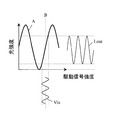
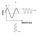
- FIG. 8 is a diagram schematically showing the operation of optical modulation by the optical module of FIG. 7.
- FIG. 8A shows the quenching characteristics of the Machzenda light modulator, which changes in a sinusoidal manner with respect to the voltage.
- Lout is an optical modulation signal output from the Machzenda light modulator.
- a drive signal Vin whose voltage changes around the bias point B is input to the Machzenda optical modulator.
- the bias point B as the intermediate point of the quenching characteristic, high linearity of the conversion characteristic between the drive signal Vin and the optical modulation signal Lout is ensured. It is a well-known fact that the light-modulated signal Lout under such operating conditions can obtain good characteristics in which signal distortion is sufficiently suppressed.
- FIG. 9 shows a structure when the driver 102 is mounted inside the housing while maintaining the basic structure of the optical module shown in FIG. 7.
- the driver 102 applies a drive signal input from the outside via the high-frequency lines 120 and 121 to the capacitively loaded high-frequency lines 116 and 117.
- the heat generated by the driver 102 is transmitted to the optical semiconductor element 101 via the gold wires 122 and 123 that electrically connect the ends of the capacitively loaded high frequency lines 116 and 117 and the driver 102, and locally causes the optical semiconductor element 101. Heat.
- the region to be locally heated is shown as the high temperature region 131. Since this local heating is applied to the region of the optical waveguide 113 of the two optical waveguides 112 and 113 constituting the Machzenda light modulator, there is a particular concern in the semiconductor material having a refractive index having a temperature characteristic. It becomes an event to be done. The reason for concern is that it disturbs the interference conditions in the Machzenda light modulator.
- FIG. 10 is a diagram schematically showing the operation of optical modulation by the optical module of FIG. After adjusting the bias point B again and obtaining a new intermediate point of the quenching characteristic, the drive signal Vin whose voltage changes around the bias point B is input to the Machzenda optical modulator.
- the bias point B As the intermediate point of the quenching characteristic, high linearity of the conversion characteristic between the drive signal Vin and the optical modulation signal Lout is ensured. Therefore, under the operating conditions shown in FIG. 10, even in the configuration shown in FIG. 9, it is possible to obtain an optical modulation signal Lout having good characteristics in which signal distortion is sufficiently suppressed.
- the present invention has been made to solve the above problems, and an object of the present invention is to realize stable operation of an optical module.
- the optical module of the present invention includes a cooling element, an optical semiconductor element mounted on the cooling element, and an active element configured to drive a high-frequency circuit of the optical semiconductor element, and the optical semiconductor element.
- the optical module of the present invention includes a cooling element, an optical semiconductor element mounted on the cooling element, and a terminator configured to terminate a high-frequency circuit of the optical semiconductor element.
- the semiconductor element includes an optical circuit having a function of an optical interferometer and the high frequency circuit formed on the surface of the optical circuit, and the cooling element has another cooling capacity in a region near the termination device. It is characterized by being higher than the cooling capacity of the region.
- the optical module of the present invention comprises a cooling element, an optical semiconductor element mounted on the cooling element, an active element configured to drive a high frequency circuit of the optical semiconductor element, and the high frequency circuit.
- the optical semiconductor device includes an optical circuit having a function of an optical interferometer and the high-frequency circuit formed on the surface of the optical circuit, and includes the cooling element. Is characterized in that the cooling capacity in the region near the active element and the region near the terminator is higher than the cooling capacity in other regions.
- the present invention by making the cooling capacity of the cooling element in the region near the active element higher than the cooling capacity in other regions, a constant heat inflow from the active element to the optical semiconductor element is generated during operation. Since the in-plane temperature distribution of the optical semiconductor device can be made uniform, fluctuations in the interference conditions of the optical interferometer can be suppressed, and stable operation of the optical module can be realized. ..
- the present invention by making the cooling capacity of the cooling element in the region near the termination device higher than the cooling capacity in other regions, a constant heat inflow from the termination device to the optical semiconductor element is generated during operation. Also, since the in-plane temperature distribution of the optical semiconductor element can be made uniform, stable operation of the optical module can be realized.
- the cooling capacity of the cooling element in the region near the active element and the region near the termination device is made higher than the cooling capacity in other regions, so that the active element and the termination device are constantly connected to the optical semiconductor device. Since the in-plane temperature distribution of the optical semiconductor element can be made uniform even during the operation in which the heat inflow is generated, the stable operation of the optical module can be realized.
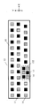
- FIG. 1 is a plan view of an optical module according to a first embodiment of the present invention.
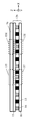
- FIG. 2A is a side view of the optical semiconductor device and the Peltier module according to the first embodiment of the present invention.
- FIG. 2B is a plan view of the Peltier module according to the first embodiment of the present invention.
- FIG. 3 is a plan view of the optical module according to the second embodiment of the present invention.
- FIG. 4A is a side view of the optical semiconductor device and the Peltier module according to the second embodiment of the present invention.
- FIG. 4B is a plan view of the Peltier module according to the second embodiment of the present invention.
- FIG. 5 is a plan view of the optical module according to the third embodiment of the present invention.
- FIG. 6A is a side view of the optical semiconductor device and the Peltier module according to the third embodiment of the present invention.
- FIG. 6B is a plan view of the Peltier module according to the third embodiment of the present invention.
- FIG. 7 is a plan view of a conventional optical module equipped with a Machzenda optical modulator.
- FIG. 8 is a diagram schematically showing the operation of optical modulation by the optical module of FIG. 7.
- FIG. 9 is a plan view of an optical module in which a driver is mounted inside a housing.
- FIG. 10 is a diagram schematically showing the operation of optical modulation by the optical module of FIG.
- FIG. 11 is a diagram schematically showing another operation of optical modulation by the optical module of FIG.
- FIG. 1 is a plan view of an optical module according to a first embodiment of the present invention.
- a Peltier module cooling element
- an optical semiconductor element 3 mounted on the Peltier module and a driver 4 for driving a high-frequency line of the optical semiconductor element 3 are driven.
- active element gold wires 5 and 6 connecting the input end of the high-frequency line of the optical semiconductor element 3 and the driver 4, the terminator 7 for terminating the high-frequency line of the optical semiconductor element 3, and the optical semiconductor element 3.
- Gold wires 8 and 9 for connecting the output end of the high frequency line and the terminator 7 are mounted.
- the optical semiconductor element 3 includes a Machzenda optical modulator 30.
- the Machzenda optical modulator 30 is composed of an optical circuit having a function of an optical interferometer and capacitively loaded high-frequency lines 37 and 38 (high-frequency circuits) formed on the surface of the optical circuit.
- the optical circuit is an optical waveguide 31, an output optical waveguide 32, two optical waveguides 33, 34, and an optical waveguide 35 that divides the light propagating through the input optical waveguide 31 into the two optical waveguides 33, 34.
- an optical waveguide 36 that combines the light propagating through the two optical waveguides 33 and 34 into the output optical waveguide 32.
- CW (Continuous Wave) light is input to the input optical waveguide 31 from the outside of the housing.
- Light modulated by the Machzenda light modulator 30 is output from the output optical waveguide 32.
- the driver 4 applies a drive signal input from the outside of the housing via the high-frequency lines 10 and 11 to the capacitively loaded high-frequency lines 37 and 38.
- the input ends of the capacitively loaded high-frequency lines 37 and 38 and the output terminals of the driver 4 are electrically connected by gold wires 5 and 6.
- Electrodes 39, 40 periodically provided on the capacitance-loaded high-frequency lines 37, 38 have a structure that adds capacitance to the high-frequency lines.
- the electrodes 39 and 40 apply a drive signal to the optical waveguides 33 and 34.
- the capacitance added to the high-frequency line by the electrodes 39 and 40 has a function of matching the group velocity of light propagating through the optical waveguides 33 and 34 with the group velocity of the drive signal (high-frequency signal).
- the output ends of the capacitively loaded high-frequency lines 37 and 38 are connected to the terminator 7 by gold wires 8 and 9.
- the drive signal propagated on the capacitively loaded high-frequency lines 37 and 38 is converted into heat in the terminator 7 without returning to the driver 4.
- the heat generated by the terminator 7 is transferred to the optical semiconductor element 3 via the gold wires 8 and 9, and locally heats the optical semiconductor element 3.
- the region heated by the heat transferred through the gold wires 8 and 9 is shown as the high temperature region 130.
- the power consumption of the driver 4 is usually in watts.
- the heat generated by the driver 4 is transferred to the optical semiconductor element 3 via the gold wires 5 and 6, and locally heats the optical semiconductor element 3.
- the region heated by the heat transferred through the gold wires 5 and 6 is shown as the high temperature region 131.
- the Peltier module provided directly under the optical semiconductor element 3 makes the in-plane temperature distribution of the optical semiconductor element 3 uniform during the operation of the optical module 1.
- FIG. 2A is a side view of the optical semiconductor element 3 and the Peltier module 12, and
- FIG. 2B is a plan view of the Peltier module 12.
- the description of the driver 4, the terminator 7, and the gold wires 5, 6, 8 and 9 is omitted.
- the description of the electrodes of the thermoelectric semiconductor of the Peltier module 12 and the like is omitted.
- FIG. 2B the inside of the Peltier module 12 is viewed through.
- a plurality of pairs of a P-type thermoelectric semiconductor 13 and an N-type thermoelectric semiconductor 14 are two-dimensionally arranged, and the P-type thermoelectric semiconductor 13 and the N-type thermoelectric semiconductor 14 are combined with each other.
- the arrangement densities of the P-type thermoelectric semiconductor 13 and the N-type thermoelectric semiconductor 14 constituting the Peltier module 12 are selectively changed. Specifically, of the in-plane region of the junction surface (the upper surface of the substrate 15 and the XY plane of FIG. 2B) of the Pelce module 12 with the optical semiconductor element 3, the high temperature region 131 of the optical semiconductor element 3 The pair of the P-type thermoelectric semiconductor 13 and the N-type thermoelectric semiconductor 14 is densely arranged in the region 132 directly below, and the pair of the P-type thermoelectric semiconductor 13 and the N-type thermoelectric semiconductor 14 is sparsely arranged in the region other than the region 132. .. With such an arrangement, in this embodiment, the cooling capacity of the Peltier module 12 is selectively changed, and the cooling capacity in the region 132 in the vicinity of the driver 4 is made higher than the cooling capacity in the other regions.
- the in-plane temperature distribution of the optical semiconductor element 3 can be made uniform during the operation of the optical module 1, it is possible to suppress fluctuations in the interference conditions of the Machzenda optical modulator 30. This enables stable operation of the Machzenda optical modulator 30.
- FIG. 3 is a plan view of the optical module according to the second embodiment of the present invention.
- a Peltier module cooling element
- an optical semiconductor element 3 mounted on the Peltier module a driver 4
- gold wires 5 and 6 and terminations are provided in the housing 2 of the optical module 1a of this embodiment.
- a vessel 7a is equipped with a vessel 7a.
- the optical semiconductor element 3, the driver 4, and the gold wires 5 and 6 are as described in the first embodiment. Similar to the first embodiment, the terminator 7a terminates the capacitively loaded high frequency lines 37 and 38 of the Machzenda optical modulator 30 of the optical semiconductor element 3.
- one end of the termination device 7a made of a thin film resistor is electrically connected to the output end of the capacitance-loaded high-frequency line 37, and the other end of the termination device 7a is the capacitance-loaded high-frequency line 38.
- the terminator 7a is formed (monolithically integrated) on the surface of the optical semiconductor element 3 so as to be electrically connected to the output end of the optical semiconductor element 3.
- one end of the terminator 7a made of discrete parts is electrically connected to the output end of the capacitively loaded high frequency line 37, and the other end of the terminator 7a is electrically connected to the output end of the capacitively loaded high frequency line 38.
- the terminator 7a may be flip-chip mounted on the surface of the optical semiconductor element 3.
- the gold wires 8 and 9 are not required, so that the reflection loss of the high frequency signal can be reduced.
- the heat generated by the terminator 7a is easily transferred to the optical semiconductor element 3.
- the region heated by the heat generated by the terminator 7a is shown as the high temperature region 133.
- the high temperature region was only one location indicated by 130, but in this embodiment, there are two locations, 130 and 133.
- the driver 4 is an open collector type, it is necessary to supply a current to the output of the driver 4 from the terminator side, so that the terminator 7a generates a large amount of heat. Since the high temperature region 133 generated by the heat generated by the terminator 7a overlaps with the region of the optical waveguide 34 of the two optical waveguides 33 and 34 constituting the Machzenda optical modulator 30, the heat generated by the terminator 7a cannot be ignored.
- the Peltier module provided directly under the optical semiconductor element 3 makes the in-plane temperature distribution of the optical semiconductor element 3 uniform during the operation of the optical module 1a.
- FIG. 4A is a side view of the optical semiconductor element 3 and the Peltier module 12a
- FIG. 4B is a plan view of the Peltier module 12a.
- the description of the driver 4, the terminator 7a, and the gold wires 5 and 6 is omitted.
- the description of the electrodes of the thermoelectric semiconductor of the Peltier module 12a and the like is omitted.
- FIG. 4B the inside of the Peltier module 12a is seen through.
- the operating principle of the Peltier module 12a is the same as that of the Peltier module 12 of the first embodiment.
- the optical semiconductor element 3 is mounted on the substrate 15 on the cooling side of the Peltier module 12a.
- the high temperature of two points of the optical semiconductor element 3 Pairs of the P-type thermoelectric semiconductor 13 and the N-type thermoelectric semiconductor 14 are densely arranged in the regions 132 and 134 directly below the regions 131 and 133, and the P-type thermoelectric semiconductor 13 and the N-type thermoelectric semiconductor 14 are arranged in regions other than the regions 132 and 134.
- the pairs of are sparsely arranged.
- the in-plane temperature distribution of the optical semiconductor element 3 can be made uniform during the operation of the optical module 1a. Fluctuations in interference conditions can be suppressed, and stable operation of the Machzenda optical modulator 30 is possible.
- the optical module in which the optical semiconductor element 3, the driver 4, and the terminator 7a are mounted in the same housing is targeted, but the driver is outside the housing as shown in FIG.
- This embodiment can also be applied to an optical module.
- the high temperature region is only one location indicated by 133.
- FIG. 5 is a plan view of the optical module according to the third embodiment of the present invention.
- a Peltier module cooling element
- an optical semiconductor element 3b mounted on the Peltier module and a driver 4 for driving a high-frequency line of the optical semiconductor element 3b are driven.
- -YQ, 6-XI, 6-XQ, 6-YI, 6-YQ and terminators 7-XI, 7-XQ, 7-YI, 7-XQ that terminate the high frequency line of the optical semiconductor element 3b are installed. Has been done.
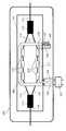
- the optical semiconductor element 3b includes a polarization multiplex optical IQ modulator.
- the polarization multiplex optical IQ modulator includes an optical demultiplexer 41 that divides the input light into two, optical waveguides 42-X and 42-Y that waveguide light from the optical demultiplexer 41, and X-biased.
- the X polarization side optical IQ modulator 43-X that polarization-modulates the input light from the optical waveguide 42-X according to the drive signal on the wave side, and the Y polarization side whose polarization state is orthogonal to the X polarization side. It is composed of a Y polarization side optical IQ modulator 43-Y that polarizes and modulates the input light from the optical waveguide 42-Y according to the driving signal of.
- the X polarization side optical IQ modulator 43-X includes an optical duplexer 44-X, an I side Mach Zender optical modulator 45-XI, a Q side Mach Zender optical modulator 45-XQ, and an optical duplexer 46-X. It is composed of and.
- the Y polarization side optical IQ modulator 43-Y includes an optical duplexer 44-Y, an I side Mach Zender optical modulator 45-YI, a Q side Mach Zender optical modulator 45-YQ, and an optical duplexer 46-Y. It is composed of and.
- the I-side Machzenda optical modulator 45-XI is composed of an optical circuit having an optical interferometer function and capacitively loaded high-frequency lines 53-XI and 54-XI (high-frequency circuits) formed on the surface of the optical circuit. Will be done.
- the optical circuit is composed of an input optical waveguide 47-XI, an output optical waveguide 48-XI, an optical waveguide 49-XI, an optical waveguide 50-XI, 51-XI, and an optical waveguide 52-XI. To.
- the Q-side Machzenda optical modulator 45-XQ is composed of an optical circuit having an optical interferometer function and capacitively loaded high-frequency lines 53-XQ and 54-XQ (high-frequency circuits) formed on the surface of the optical circuit. Will be done.
- the optical circuit is composed of an input optical waveguide 47-XQ, an output optical waveguide 48-XQ, an optical waveguide 49-XQ, an optical waveguide 50-XQ, 51-XQ, and an optical waveguide 52-XQ. To.
- the I-side Machzenda optical modulator 45-YI is composed of an optical circuit having an optical interferometer function and capacitively loaded high-frequency lines 53-YI and 54-YI (high-frequency circuits) formed on the surface of the optical circuit. Will be done.
- the optical circuit is composed of an input optical waveguide 47-YI, an output optical waveguide 48-YI, an optical waveguide 49-YI, an optical waveguide 50-YI, 51-YI, and an optical waveguide 52-YI. To.
- the Q-side Machzenda optical modulator 45-YQ is composed of an optical circuit having an optical interferometer function and capacitively loaded high-frequency lines 53-YQ and 54-YQ (high-frequency circuits) formed on the surface of the optical circuit. Will be done.
- the optical circuit is composed of an input optical waveguide 47-YQ, an output optical waveguide 48-YQ, an optical waveguide 49-YQ, an optical waveguide 50-YQ, 51-YQ, and an optical waveguide 52-YQ. To.
- the optical demultiplexer 41 divides the CW light input from the outside of the housing into two.
- the optical demultiplexer 44-X of the X polarization side optical IQ modulator 43-X divides the input light from the optical demultiplexer 41 into two.
- the optical duplexer 49-XI of the I-side Machzenda light modulator 45-XI splits the input light from the optical modulator 44-X into two.
- the driver 4-X receives the drive signal input from the outside of the housing via the high-frequency lines 10-XI and 11-XI to the capacitively loaded high-frequency lines 53-XI and 54- of the I-side Mach Zender optical modulator 45-XI. Apply to XI.
- the input terminals of the capacitively loaded high-frequency lines 53-XI and 54-XI and the output terminals of the driver 4-X are electrically connected by gold wires 5-XI and 6-XI.
- Electrodes periodically provided on the capacitively loaded high-frequency lines 53-XI and 54-XI apply drive signals to the optical waveguides 50-XI and 51-XI. By applying the drive signal, the light propagating through the optical waveguides 50-XI and 51-XI is modulated.
- the optical combiner 52-XI combines the light propagating through the optical waveguides 50-XI and 51-XI into the output optical waveguide 48-XI.
- the optical demultiplexer 49-XQ of the Q-side Mach Zender optical modulator 45-XQ splits the input light from the optical demultiplexer 44-X into two.
- the driver 4-X receives the drive signal input from the outside of the housing via the high-frequency lines 10-XQ and 11-XQ to the capacitively loaded high-frequency lines 53-XQ and 54- of the Q-side Mach Zender optical modulator 45-XQ. Apply to XQ.
- the input terminals of the capacitively loaded high-frequency lines 53-XQ and 54-XQ and the output terminals of the driver 4-X are electrically connected by gold wires 5-XQ and 6-XQ.
- Electrodes periodically provided on the capacitively loaded high-frequency lines 53-XQ and 54-XQ apply drive signals to the optical waveguides 50-XQ and 51-XQ.
- the optical combiner 52-XQ combines the light propagating through the optical waveguides 50-XQ and 51-XQ with the output optical waveguide 48-XQ.
- the optical modulator 46-X combines the light output from the I-side Machzender optical modulator 45-XI with the light output from the Q-side Machzenda optical modulator 45-XQ.
- the optical demultiplexer 44-Y of the Y polarization side optical IQ modulator 43-Y divides the input light from the optical demultiplexer 41 into two.
- the optical duplexer 49-YI of the I-side Machzenda light modulator 45-YI splits the input light from the optical modulator 44-Y into two.
- the driver 4-Y receives the drive signal input from the outside of the housing via the high-frequency lines 10-YI and 11-YI to the capacitively loaded high-frequency lines 53-YI and 54- of the I-side Machzenda optical modulator 45-YI. Apply to YI.
- the input terminals of the capacitively loaded high-frequency lines 53-YI and 54-YI and the output terminals of the driver 4-Y are electrically connected by gold wires 5-YI and 6-YI.
- Electrodes periodically provided on the capacitively loaded high-frequency lines 53-YI and 54-YI apply drive signals to the optical waveguides 50-YI and 51-YI. By applying the drive signal, the light propagating through the optical waveguides 50-YI and 51-YI is modulated.
- the optical combiner 52-YI combines the light propagating through the optical waveguides 50-YI and 51-YI with the output optical waveguide 48-YI.
- the optical demultiplexer 49-YQ of the Q-side Mach Zender optical modulator 45-YQ splits the input light from the optical demultiplexer 44-Y into two.
- the driver 4-Y receives the drive signal input from the outside of the housing via the high-frequency lines 10-YQ and 11-YQ to the capacitively loaded high-frequency lines 53-YQ and 54- of the Q-side Machzenda optical modulator 45-YQ. Apply to YQ.
- the input ends of the capacitively loaded high-frequency lines 53-YQ and 54-YQ and the output terminals of the driver 4-Y are electrically connected by gold wires 5-YQ and 6-YQ.
- Electrodes periodically provided on the capacitively loaded high-frequency lines 53-YQ and 54-YQ apply drive signals to the optical waveguides 50-YQ and 51-YQ.
- the optical combiner 52-YQ combines the light propagating in the optical waveguides 50-YQ and 51-YQ into the output optical waveguide 48-YQ.
- the optical modulator 46-Y combines the light output from the I-side Machzender optical modulator 45-YI with the light output from the Q-side Machzenda optical modulator 45-YQ.
- the terminator 7-XI terminates the capacitively loaded high frequency lines 53-XI and 54-XI of the I-side Machzenda optical modulator 45-XI.
- the terminator 7-XQ terminates the capacitively loaded high frequency lines 53-XQ and 54-XQ of the Q-side Mach Zender optical modulator 45-XQ.
- the terminator 7-YI terminates the capacitively loaded high frequency lines 53-YI and 54-YI of the I-side Machzenda optical modulator 45-YI.
- the terminator 7-YQ terminates the capacitively loaded high-frequency lines 53-YQ and 54-YQ of the Q-side Machzenda optical modulator 45-YQ.
- One end of the terminator 7-XI made of a thin film resistor is electrically connected to the output end of the capacitively loaded high frequency line 53-XI, and the other end of the terminator 7-X is the output of the capacitively loaded high frequency line 54-XI.
- a terminator 7-X is formed (monolithic integration) on the surface of the optical semiconductor element 3b so as to be electrically connected to the end.
- one end of the terminator 7-X made of discrete components is electrically connected to the output end of the capacitively loaded high frequency line 53-XI, and the other end of the terminator 7-X is of the capacitively loaded high frequency line 54-XI.
- the terminator 7-X may be flip-chip mounted on the surface of the optical semiconductor device 3b so as to be electrically connected to the output end.
- the terminators 7-XQ, 7-YI, and 7-YQ are monolithically integrated or flip-chip mounted on the surface of the optical semiconductor device 3b.
- the number of drivers is increased to two and the number of terminators is increased to four, so that the number of heat generating points is increased and the drivers are terminated with 4-X and 4-Y.
- the high temperature regions 135 and 136 generated by the heat generated by the vessels 7-XI, 7-XQ, 7-YI and 7-XQ are also expanded.
- FIG. 6A is a side view of the optical semiconductor element 3b and the Peltier module 12b
- FIG. 6B is a plan view of the Peltier module 12b.
- the description of -XI, 6-XQ, 6-YI, 6-YQ is omitted.
- FIG. 6A the description of the electrodes of the thermoelectric semiconductor of the Peltier module 12b and the like is omitted.
- FIG. 6B the inside of the Peltier module 12b is viewed through.
- the operating principle of the Peltier module 12b is the same as that of the Peltier module 12 of the first embodiment.
- the optical semiconductor element 3b is mounted on the substrate 15 on the cooling side of the Peltier module 12b.
- the high temperature of two points of the optical semiconductor element 3b Pairs of the P-type thermoelectric semiconductor 13 and the N-type thermoelectric semiconductor 14 are densely arranged in the regions 137 and 138 directly below the regions 135 and 136, and the P-type thermoelectric semiconductor 13 and the N-type thermoelectric semiconductor 14 are arranged in regions other than the regions 137 and 138.
- the pairs of are sparsely arranged.
- the cooling capacity of the Peltier module 12b is selectively changed, and the region 137 in the vicinity of the drivers 4-X and 4-Y and the terminators 7-XI, 7-XQ, 7-
- the cooling capacity in the region 138 near YI, 7-XQ is higher than the cooling capacity in the other regions.
- the in-plane temperature distribution of the optical semiconductor element 3b can be made uniform during the operation of the optical module 1b, so that the I-side Machzenda light modulator Fluctuations in the interference conditions of the 45-XI, 45-YI and Q-side Machzenda optical modulators 45-XQ and 45-YQ can be suppressed, and the I-side Machzenda optical modulators 45-XI, 45-YI and Q can be suppressed.
- the stable operation of the side Mach Zender optical modulators 45-XQ and 45-YQ is possible.
- an optical module in which an optical semiconductor element 3b, a driver 4-X, 4-Y, and a terminator 7-XI, 7-XQ, 7-YI, 7-XQ are mounted in the same housing is used.
- the present embodiment can also be applied to an optical module in which the driver is outside the housing. In this case, the high temperature region is only one location indicated by 136.
- the semiconductor materials constituting the Machzenda optical modulators 30, 45-XI, 45-YI, 45-XQ, and 45-YQ it is not necessary to particularly limit the semiconductor materials constituting the Machzenda optical modulators 30, 45-XI, 45-YI, 45-XQ, and 45-YQ.
- Various semiconductor materials such as InGaAsP / InP system or GaAs / GaAlAs system can be applied to Machzenda light modulators 30, 45-XI, 45-YI, 45-XQ, 45-YQ.
- the cross-sectional structure of the optical waveguide constituting the Machzenda optical modulators 30, 45-XI, 45-YI, 45-XQ, and 45-YQ does not need to be particularly limited.
- Various optical waveguide structures such as high mesa type, ridge type, and rib type can be applied.
- drivers 4,4-X, 4-Y and optical semiconductor elements 3, 3b are integrated
- modulation efficiency is improved. From the viewpoint, it is not necessary to match with single-phase 50 ⁇ and differential 100 ⁇ .
- the arrangement of the pair of the P-type thermoelectric semiconductor 13 and the N-type thermoelectric semiconductor 14 of the Peltier modules 12, 12a and 12b is not limited to the arrangement shown in the first to third embodiments.
- P-type thermoelectric semiconductors 13 and N so that the non-uniformity of the in-plane temperature distribution of the optical semiconductor devices 3, 3b in the high temperature regions 131, 133, 135, 136 can be grasped in advance and this non-uniformity can be eliminated.
- a pair of type thermoelectric semiconductors 14 may be arranged.
- pairs of the P-type thermoelectric semiconductor 13 and the N-type thermoelectric semiconductor 14 are arranged in substantially the same pattern in the regions 132 and 134, but due to the difference in temperature in the high temperature regions 131 and 133 directly above the regions, the regions It goes without saying that 132 and 134 may be arranged in different patterns.
- the pair of the P-type thermoelectric semiconductor 13 and the N-type thermoelectric semiconductor 14 are arranged in the same pattern in the regions 137 and 138, but it goes without saying that they may be arranged in different patterns. No.
- the arrangement of the pair of the P-type thermoelectric semiconductor 13 and the N-type thermoelectric semiconductor 14 is divided into two stages of sparse and dense. Needless to say, the density of the pair of the P-type thermoelectric semiconductor 13 and the N-type thermoelectric semiconductor 14 may change in a plurality of steps in the regions 132, 134, 137, and 138 immediately below.
- the high temperature regions of the optical semiconductor elements 3 and 3b are set to two locations each, but similarly, even when there are three or more high temperature regions, the optical semiconductor element A pair of the P-type thermoelectric semiconductor 13 and the N-type thermoelectric semiconductor 14 may be arranged so that the non-uniformity of the in-plane temperature distribution can be eliminated.
- the present invention can be applied to an optical module equipped with an optical modulator.
- thermoelectric semiconductor 1,1a, 1b ...
- Optical module 2 ... Housing, 3,3b ...
- Optical semiconductor element 4,4-X, 4-Y ... Driver, 5,5-XI, 5-XQ, 5-YI, 5- YQ, 6,6-XI, 6-XQ, 6-YI, 6-YQ ... Gold wire, 7,7a, 7-XI, 7-XQ, 7-YI, 7-XQ ... Terminator, 12, 12a, 12b ... Perche module, 13 ...
- P-type thermoelectric semiconductor 14 ... N-type thermoelectric semiconductor, 30 ... Machzenda light modulator, 31,47-XI, 47-XQ, 47-YI, 47-YQ ...
- Input optical waveguide 32, 48-XI, 48-XQ, 48-YI, 48-YQ ...
- Optical Waveguide 37, 38, 53-XI, 53-XQ, 53-YI, 53-YQ, 54-XI, 54-XQ, 54-YI, 54-YQ ... Capacitive loaded high frequency line, 39, 40 ... Electrodes, 43-X ... X polarization side optical IQ modulator, 43-Y ... Y polarization side light IQ modulators, 45-XI, 45-YI ... I-side Machzenda optical modulators, 45-XQ, 45-YQ ... Q-side Machzenda optical modulators.
Landscapes
- Physics & Mathematics (AREA)
- Nonlinear Science (AREA)
- General Physics & Mathematics (AREA)
- Optics & Photonics (AREA)
- Electromagnetism (AREA)
- Optical Modulation, Optical Deflection, Nonlinear Optics, Optical Demodulation, Optical Logic Elements (AREA)
Abstract
Description
図11のケースでは、バイアス点Bが消光特性の中間点に設定されなかった場合を示している。このとき、図11で明らかなように光変調信号Loutに歪みが生じ、マッハツェンダ光変調器を光送信器に用いる場合の信号品質が劣化する。
図1は本発明の第1の実施例に係る光モジュールの平面図である。本実施例の光モジュール1の筐体2内には、後述するペルチェモジュール(冷却素子)と、ペルチェモジュール上に搭載された光半導体素子3と、光半導体素子3の高周波線路を駆動するドライバ4(能動素子)と、光半導体素子3の高周波線路の入力端とドライバ4とを接続する金ワイヤ5,6と、光半導体素子3の高周波線路を終端する終端器7と、光半導体素子3の高周波線路の出力端と終端器7とを接続する金ワイヤ8,9とが搭載されている。
ドライバ4は、筐体外部から高周波線路10,11を介して入力された駆動信号を、容量装荷型高周波線路37,38に印加する。容量装荷型高周波線路37,38の入力端とドライバ4の出力端子との間は、金ワイヤ5,6によって電気的に接続されている。
図2Aは光半導体素子3とペルチェモジュール12の側面図、図2Bはペルチェモジュール12の平面図である。なお、図2Aでは、ドライバ4と終端器7と金ワイヤ5,6,8,9の記載を省略している。また、図2Aでは、ペルチェモジュール12の熱電半導体の電極等の記載を省略している。図2Bでは、ペルチェモジュール12の内部を透視して記載している。
次に、本発明の第2の実施例について説明する。図3は本発明の第2の実施例に係る光モジュールの平面図である。本実施例の光モジュール1aの筐体2内には、後述するペルチェモジュール(冷却素子)と、ペルチェモジュール上に搭載された光半導体素子3と、ドライバ4と、金ワイヤ5,6と、終端器7aとが搭載されている。
第1の実施例と同様に、終端器7aは、光半導体素子3のマッハツェンダ光変調器30の容量装荷型高周波線路37,38を終端する。第1の実施例との違いは、薄膜抵抗器からなる終端器7aの一端が容量装荷型高周波線路37の出力端と電気的に接続され、終端器7aの他端が容量装荷型高周波線路38の出力端と電気的に接続されるように、終端器7aが光半導体素子3の表面に形成(モノリシック集積)されていることである。あるいは、ディスクリート部品からなる終端器7aの一端が容量装荷型高周波線路37の出力端と電気的に接続され、終端器7aの他端が容量装荷型高周波線路38の出力端と電気的に接続されるように、終端器7aを光半導体素子3の表面上にフリップチップ実装してもよい。
ただし、終端器7aで生じた熱は光半導体素子3に容易に伝わる。図3では、終端器7aの発熱によって加熱される領域を、高温度領域133として示している。
次に、本発明の第3の実施例について説明する。図5は本発明の第3の実施例に係る光モジュールの平面図である。本実施例の光モジュール1bの筐体2内には、後述するペルチェモジュール(冷却素子)と、ペルチェモジュール上に搭載された光半導体素子3bと、光半導体素子3bの高周波線路を駆動するドライバ4-X,4-Y(能動素子)と、光半導体素子3bの高周波線路の入力端とドライバ4-X,4-Yとを接続する金ワイヤ5-XI,5-XQ,5-YI,5-YQ,6-XI,6-XQ,6-YI,6-YQと、光半導体素子3bの高周波線路を終端する終端器7-XI,7-XQ,7-YI,7-XQとが搭載されている。
Y偏波側光IQ変調器43-Yは、光分波器44-Yと、I側マッハツェンダ光変調器45-YIと、Q側マッハツェンダ光変調器45-YQと、光合波器46-Yとから構成される。
I側マッハツェンダ光変調器45-XIの光分波器49-XIは、光分波器44-Xからの入力光を2つに分波する。ドライバ4-Xは、筐体外部から高周波線路10-XI,11-XIを介して入力された駆動信号を、I側マッハツェンダ光変調器45-XIの容量装荷型高周波線路53-XI,54-XIに印加する。容量装荷型高周波線路53-XI,54-XIの入力端とドライバ4-Xの出力端子との間は、金ワイヤ5-XI,6-XIによって電気的に接続されている。
光合波器52-XIは、光導波路50-XI,51-XIを伝搬する光を出力光導波路48-XIへと合波する。
光合波器46-Xは、I側マッハツェンダ光変調器45-XIから出力された光とQ側マッハツェンダ光変調器45-XQから出力された光とを合波する。
I側マッハツェンダ光変調器45-YIの光分波器49-YIは、光分波器44-Yからの入力光を2つに分波する。ドライバ4-Yは、筐体外部から高周波線路10-YI,11-YIを介して入力された駆動信号を、I側マッハツェンダ光変調器45-YIの容量装荷型高周波線路53-YI,54-YIに印加する。容量装荷型高周波線路53-YI,54-YIの入力端とドライバ4-Yの出力端子との間は、金ワイヤ5-YI,6-YIによって電気的に接続されている。
光合波器52-YIは、光導波路50-YI,51-YIを伝搬する光を出力光導波路48-YIへと合波する。
光合波器46-Yは、I側マッハツェンダ光変調器45-YIから出力された光とQ側マッハツェンダ光変調器45-YQから出力された光とを合波する。
Claims (8)
- 冷却素子と、
前記冷却素子の上に搭載された光半導体素子と、
前記光半導体素子の高周波回路を駆動するように構成された能動素子とを備え、
前記光半導体素子は、
光干渉計の機能を備えた光回路と、
前記光回路の表面に形成された前記高周波回路とを備え、
前記冷却素子は、前記能動素子の近傍領域での冷却能力が他の領域の冷却能力よりも高いことを特徴とする光モジュール。 - 請求項1記載の光モジュールにおいて、
前記冷却素子は、前記光半導体素子との接合面の面内方向に沿ってP型熱電半導体とN型熱電半導体の対を2次元的に配置したペルチェモジュールであり、前記面内方向の領域のうち、前記能動素子の近傍領域での前記P型熱電半導体と前記N型熱電半導体の対の密度が、他の領域での前記P型熱電半導体と前記N型熱電半導体の対の密度よりも高いことを特徴とする光モジュール。 - 冷却素子と、
前記冷却素子の上に搭載された光半導体素子と、
前記光半導体素子の高周波回路を終端するように構成された終端器とを備え、
前記光半導体素子は、
光干渉計の機能を備えた光回路と、
前記光回路の表面に形成された前記高周波回路とを備え、
前記冷却素子は、前記終端器の近傍領域での冷却能力が他の領域の冷却能力よりも高いことを特徴とする光モジュール。 - 請求項3記載の光モジュールにおいて、
前記冷却素子は、前記光半導体素子との接合面の面内方向に沿ってP型熱電半導体とN型熱電半導体の対を2次元的に配置したペルチェモジュールであり、前記面内方向の領域のうち、前記終端器の近傍領域での前記P型熱電半導体と前記N型熱電半導体の対の密度が、他の領域での前記P型熱電半導体と前記N型熱電半導体の対の密度よりも高いことを特徴とする光モジュール。 - 冷却素子と、
前記冷却素子の上に搭載された光半導体素子と、
前記光半導体素子の高周波回路を駆動するように構成された能動素子と、
前記高周波回路を終端するように構成された終端器とを備え、
前記光半導体素子は、
光干渉計の機能を備えた光回路と、
前記光回路の表面に形成された前記高周波回路とを備え、
前記冷却素子は、前記能動素子の近傍領域と前記終端器の近傍領域での冷却能力が他の領域の冷却能力よりも高いことを特徴とする光モジュール。 - 請求項5記載の光モジュールにおいて、
前記冷却素子は、前記光半導体素子との接合面の面内方向に沿ってP型熱電半導体とN型熱電半導体の対を2次元的に配置したペルチェモジュールであり、前記面内方向の領域のうち、前記能動素子の近傍領域と前記終端器の近傍領域での前記P型熱電半導体と前記N型熱電半導体の対の密度が、他の領域での前記P型熱電半導体と前記N型熱電半導体の対の密度よりも高いことを特徴とする光モジュール。 - 請求項3乃至6のいずれか1項に記載の光モジュールにおいて、
前記終端器は、前記光半導体素子の表面にモノリシック集積、または前記光半導体素子の表面上にフリップチップ実装されていることを特徴とする光モジュール。 - 請求項1乃至7のいずれか1項に記載の光モジュールにおいて、
前記光回路と前記高周波回路とは、マッハツェンダ光変調器を構成することを特徴とする光モジュール。
Priority Applications (6)
| Application Number | Priority Date | Filing Date | Title |
|---|---|---|---|
| CN201980101868.1A CN114616513A (zh) | 2019-10-29 | 2019-10-29 | 光模块 |
| PCT/JP2019/042294 WO2021084602A1 (ja) | 2019-10-29 | 2019-10-29 | 光モジュール |
| JP2021553919A JPWO2021084602A1 (ja) | 2019-10-29 | 2019-10-29 | |
| EP19951167.6A EP4053617A4 (en) | 2019-10-29 | 2019-10-29 | OPTICAL MODULE |
| CA3159066A CA3159066A1 (en) | 2019-10-29 | 2019-10-29 | Optical module |
| US17/772,891 US20220357629A1 (en) | 2019-10-29 | 2019-10-29 | Optical Module |
Applications Claiming Priority (1)
| Application Number | Priority Date | Filing Date | Title |
|---|---|---|---|
| PCT/JP2019/042294 WO2021084602A1 (ja) | 2019-10-29 | 2019-10-29 | 光モジュール |
Publications (1)
| Publication Number | Publication Date |
|---|---|
| WO2021084602A1 true WO2021084602A1 (ja) | 2021-05-06 |
Family
ID=75715883
Family Applications (1)
| Application Number | Title | Priority Date | Filing Date |
|---|---|---|---|
| PCT/JP2019/042294 WO2021084602A1 (ja) | 2019-10-29 | 2019-10-29 | 光モジュール |
Country Status (6)
| Country | Link |
|---|---|
| US (1) | US20220357629A1 (ja) |
| EP (1) | EP4053617A4 (ja) |
| JP (1) | JPWO2021084602A1 (ja) |
| CN (1) | CN114616513A (ja) |
| CA (1) | CA3159066A1 (ja) |
| WO (1) | WO2021084602A1 (ja) |
Cited By (6)
| Publication number | Priority date | Publication date | Assignee | Title |
|---|---|---|---|---|
| WO2024075167A1 (ja) * | 2022-10-03 | 2024-04-11 | 日本電信電話株式会社 | 光送信器 |
| WO2024075169A1 (ja) * | 2022-10-03 | 2024-04-11 | 日本電信電話株式会社 | 光送信器 |
| WO2024075166A1 (ja) * | 2022-10-03 | 2024-04-11 | 日本電信電話株式会社 | 光送信器 |
| WO2024075170A1 (ja) * | 2022-10-03 | 2024-04-11 | 日本電信電話株式会社 | 光送信器 |
| WO2024075168A1 (ja) * | 2022-10-03 | 2024-04-11 | 日本電信電話株式会社 | 光送信器 |
| WO2024075171A1 (ja) * | 2022-10-03 | 2024-04-11 | 日本電信電話株式会社 | 光送信器 |
Citations (5)
| Publication number | Priority date | Publication date | Assignee | Title |
|---|---|---|---|---|
| JP2003222826A (ja) * | 2002-01-29 | 2003-08-08 | Hitachi Ltd | 光送信モジュール |
| JP2004228432A (ja) * | 2003-01-24 | 2004-08-12 | Anritsu Corp | 半導体レーザモジュール及び電子冷却ユニット |
| US20050053377A1 (en) * | 2003-09-04 | 2005-03-10 | Yoo Sung-Joo Ben | Reconfigurable multi-channel all-optical regenerators |
| JP2005234267A (ja) * | 2004-02-20 | 2005-09-02 | Mitsubishi Electric Corp | 半導体光モジュール |
| JP2013156352A (ja) * | 2012-01-27 | 2013-08-15 | Japan Oclaro Inc | 光変調器及び光送信モジュール |
Family Cites Families (4)
| Publication number | Priority date | Publication date | Assignee | Title |
|---|---|---|---|---|
| JPH1073791A (ja) * | 1996-08-30 | 1998-03-17 | Hitachi Ltd | 半導体マッハツェンダ型光変調器、光変調器モジュールおよび光伝送装置 |
| JP6136363B2 (ja) * | 2013-02-27 | 2017-05-31 | 住友電気工業株式会社 | 光変調モジュール |
| JP6217243B2 (ja) * | 2013-08-29 | 2017-10-25 | 富士通オプティカルコンポーネンツ株式会社 | 光モジュールおよび光送信機 |
| JP7135382B2 (ja) * | 2018-03-30 | 2022-09-13 | 住友大阪セメント株式会社 | 光変調器、及び光送信装置 |
-
2019
- 2019-10-29 WO PCT/JP2019/042294 patent/WO2021084602A1/ja unknown
- 2019-10-29 JP JP2021553919A patent/JPWO2021084602A1/ja active Pending
- 2019-10-29 EP EP19951167.6A patent/EP4053617A4/en active Pending
- 2019-10-29 CA CA3159066A patent/CA3159066A1/en active Pending
- 2019-10-29 CN CN201980101868.1A patent/CN114616513A/zh active Pending
- 2019-10-29 US US17/772,891 patent/US20220357629A1/en active Pending
Patent Citations (5)
| Publication number | Priority date | Publication date | Assignee | Title |
|---|---|---|---|---|
| JP2003222826A (ja) * | 2002-01-29 | 2003-08-08 | Hitachi Ltd | 光送信モジュール |
| JP2004228432A (ja) * | 2003-01-24 | 2004-08-12 | Anritsu Corp | 半導体レーザモジュール及び電子冷却ユニット |
| US20050053377A1 (en) * | 2003-09-04 | 2005-03-10 | Yoo Sung-Joo Ben | Reconfigurable multi-channel all-optical regenerators |
| JP2005234267A (ja) * | 2004-02-20 | 2005-09-02 | Mitsubishi Electric Corp | 半導体光モジュール |
| JP2013156352A (ja) * | 2012-01-27 | 2013-08-15 | Japan Oclaro Inc | 光変調器及び光送信モジュール |
Non-Patent Citations (2)
| Title |
|---|
| K. PROSYKA. AIT-OUALIJ. CHENM. HAMACHERD. HOFFMANNR. KAISERR. MILLETTA. PIRASTUM. TOTOLOK. VELTHAUS: "Travelling Wave Mach-Zehnder Modulators", PROCEEDINGS INT. CONF. ON INP AND RELATED MATERIALS, KOBE, JAPAN, MOD, 1 March 2013 (2013-03-01) |
| See also references of EP4053617A4 |
Cited By (6)
| Publication number | Priority date | Publication date | Assignee | Title |
|---|---|---|---|---|
| WO2024075167A1 (ja) * | 2022-10-03 | 2024-04-11 | 日本電信電話株式会社 | 光送信器 |
| WO2024075169A1 (ja) * | 2022-10-03 | 2024-04-11 | 日本電信電話株式会社 | 光送信器 |
| WO2024075166A1 (ja) * | 2022-10-03 | 2024-04-11 | 日本電信電話株式会社 | 光送信器 |
| WO2024075170A1 (ja) * | 2022-10-03 | 2024-04-11 | 日本電信電話株式会社 | 光送信器 |
| WO2024075168A1 (ja) * | 2022-10-03 | 2024-04-11 | 日本電信電話株式会社 | 光送信器 |
| WO2024075171A1 (ja) * | 2022-10-03 | 2024-04-11 | 日本電信電話株式会社 | 光送信器 |
Also Published As
| Publication number | Publication date |
|---|---|
| EP4053617A1 (en) | 2022-09-07 |
| CN114616513A (zh) | 2022-06-10 |
| JPWO2021084602A1 (ja) | 2021-05-06 |
| EP4053617A4 (en) | 2023-07-12 |
| US20220357629A1 (en) | 2022-11-10 |
| CA3159066A1 (en) | 2021-05-06 |
Similar Documents
| Publication | Publication Date | Title |
|---|---|---|
| WO2021084602A1 (ja) | 光モジュール | |
| US11067839B2 (en) | Opto-electronic modulator utilizing one or more heating elements | |
| JP5729303B2 (ja) | 光変調器モジュール及び光信号の変調方法 | |
| JP6884850B2 (ja) | Iq光変調器 | |
| JP7267202B2 (ja) | 変調電極に対して横方向に変位した伝導平面を有する高周波光変調器 | |
| JP5267105B2 (ja) | 光モジュール及びその製造方法、光送信器 | |
| WO2012077337A1 (ja) | 光信号制御装置及び光信号制御方法 | |
| US6590691B1 (en) | Hybridly integrated optical modulation devices | |
| US9235066B2 (en) | Optical modulator | |
| CN114167555B (zh) | 一种面向高速光通信的6.4 Tbps硅基光引擎收发芯片组件 | |
| CN112003648A (zh) | 集成光发射器件 | |
| US6618179B2 (en) | Mach-Zehnder modulator with individually optimized couplers for optical splitting at the input and optical combining at the output | |
| US10394059B1 (en) | Thermo-optic phase shifter with thermal bridge | |
| JP5983839B2 (ja) | 光変調器 | |
| JPH11237593A (ja) | 光変調器 | |
| JP7388021B2 (ja) | 光デバイス | |
| US20220365377A1 (en) | Optical Circuit | |
| CN118112827A (zh) | 调制器、光模块、光通信设备及系统 |
Legal Events
| Date | Code | Title | Description |
|---|---|---|---|
| 121 | Ep: the epo has been informed by wipo that ep was designated in this application |
Ref document number: 19951167 Country of ref document: EP Kind code of ref document: A1 |
|
| ENP | Entry into the national phase |
Ref document number: 2021553919 Country of ref document: JP Kind code of ref document: A |
|
| ENP | Entry into the national phase |
Ref document number: 3159066 Country of ref document: CA |
|
| NENP | Non-entry into the national phase |
Ref country code: DE |
|
| ENP | Entry into the national phase |
Ref document number: 2019951167 Country of ref document: EP Effective date: 20220530 |