WO2024070518A1 - 配線基板 - Google Patents
配線基板 Download PDFInfo
- Publication number
- WO2024070518A1 WO2024070518A1 PCT/JP2023/032240 JP2023032240W WO2024070518A1 WO 2024070518 A1 WO2024070518 A1 WO 2024070518A1 JP 2023032240 W JP2023032240 W JP 2023032240W WO 2024070518 A1 WO2024070518 A1 WO 2024070518A1
- Authority
- WO
- WIPO (PCT)
- Prior art keywords
- wiring
- substrate
- main surface
- wiring board
- wirings
- Prior art date
- Legal status (The legal status is an assumption and is not a legal conclusion. Google has not performed a legal analysis and makes no representation as to the accuracy of the status listed.)
- Ceased
Links
Images


Classifications
-
- H—ELECTRICITY
- H05—ELECTRIC TECHNIQUES NOT OTHERWISE PROVIDED FOR
- H05K—PRINTED CIRCUITS; CASINGS OR CONSTRUCTIONAL DETAILS OF ELECTRIC APPARATUS; MANUFACTURE OF ASSEMBLAGES OF ELECTRICAL COMPONENTS
- H05K1/00—Printed circuits
- H05K1/02—Details
- H05K1/14—Structural association of two or more printed circuits
- H05K1/142—Arrangements of planar printed circuit boards in the same plane, e.g. auxiliary printed circuit insert mounted in a main printed circuit
-
- H—ELECTRICITY
- H05—ELECTRIC TECHNIQUES NOT OTHERWISE PROVIDED FOR
- H05K—PRINTED CIRCUITS; CASINGS OR CONSTRUCTIONAL DETAILS OF ELECTRIC APPARATUS; MANUFACTURE OF ASSEMBLAGES OF ELECTRICAL COMPONENTS
- H05K1/00—Printed circuits
- H05K1/02—Details
-
- H—ELECTRICITY
- H05—ELECTRIC TECHNIQUES NOT OTHERWISE PROVIDED FOR
- H05K—PRINTED CIRCUITS; CASINGS OR CONSTRUCTIONAL DETAILS OF ELECTRIC APPARATUS; MANUFACTURE OF ASSEMBLAGES OF ELECTRICAL COMPONENTS
- H05K1/00—Printed circuits
- H05K1/02—Details
- H05K1/0277—Bendability or stretchability details
- H05K1/0283—Stretchable printed circuits
-
- H—ELECTRICITY
- H05—ELECTRIC TECHNIQUES NOT OTHERWISE PROVIDED FOR
- H05K—PRINTED CIRCUITS; CASINGS OR CONSTRUCTIONAL DETAILS OF ELECTRIC APPARATUS; MANUFACTURE OF ASSEMBLAGES OF ELECTRICAL COMPONENTS
- H05K1/00—Printed circuits
- H05K1/02—Details
- H05K1/14—Structural association of two or more printed circuits
-
- H—ELECTRICITY
- H05—ELECTRIC TECHNIQUES NOT OTHERWISE PROVIDED FOR
- H05K—PRINTED CIRCUITS; CASINGS OR CONSTRUCTIONAL DETAILS OF ELECTRIC APPARATUS; MANUFACTURE OF ASSEMBLAGES OF ELECTRICAL COMPONENTS
- H05K2201/00—Indexing scheme relating to printed circuits covered by H05K1/00
- H05K2201/01—Dielectrics
- H05K2201/0104—Properties and characteristics in general
- H05K2201/0129—Thermoplastic polymer, e.g. auto-adhesive layer; Shaping of thermoplastic polymer
-
- H—ELECTRICITY
- H05—ELECTRIC TECHNIQUES NOT OTHERWISE PROVIDED FOR
- H05K—PRINTED CIRCUITS; CASINGS OR CONSTRUCTIONAL DETAILS OF ELECTRIC APPARATUS; MANUFACTURE OF ASSEMBLAGES OF ELECTRICAL COMPONENTS
- H05K2201/00—Indexing scheme relating to printed circuits covered by H05K1/00
- H05K2201/09—Shape and layout
- H05K2201/09209—Shape and layout details of conductors
- H05K2201/09218—Conductive traces
- H05K2201/09236—Parallel layout
Definitions
- This disclosure relates to a wiring board.
- a conventional wiring board is described in JP-A-7-94861 (Patent Document 1).
- This wiring board is made by forming a heat-adhesive insulating resist on a first substrate and a second substrate, forming an electrode pattern on the insulating resist, and pressing the electrode patterns of the substrates against each other, and then heat-adhering the resist around the electrode pattern in the pressed state.
- the wiring board has two layers of insulating resist between the first substrate and the second substrate. The first substrate and the second substrate are connected via the two layers of insulating resist.
- the purpose of this disclosure is to provide a wiring board that can be made thinner.
- a wiring board comprises: A first substrate having a first major surface; a second substrate having a second major surface; A first wiring disposed on the first main surface; a second wiring disposed on the second main surface, the first main surface and the second main surface are in contact with each other, and the first base material and the second base material are connected to each other; The first wiring and the second wiring are electrically connected to each other and opposed to each other in a thickness direction of the first base material.
- the wiring board according to one aspect of the present invention can be made thinner.
- FIG. 1 is an exploded perspective view of a wiring board according to a first embodiment of the present invention.
- FIG. 2 is an exploded plan view of the wiring board.
- FIG. 3 is a plan view of the wiring board.
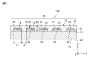
- FIG. 4 is a cross-sectional view taken along line IV-IV of FIG.
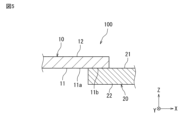
- FIG. 5 is a cross-sectional view taken along line VV of FIG.
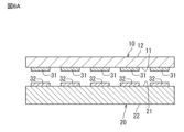
- FIG. 6A is a cross-sectional view illustrating a method for manufacturing a wiring board.
- FIG. 6B is a cross-sectional view illustrating the method for manufacturing the wiring board.
- FIG. 7 is a cross-sectional view of a wiring board according to a second embodiment of the present invention.
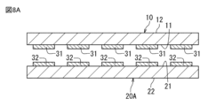
- FIG. 8A is a cross-sectional view illustrating a method for manufacturing a wiring board.
- FIG. 8B is a cross-sectional view illustrating the method for manufacturing the wiring board.
- FIG. 9 is a plan view of a wiring board according to a third embodiment of the present invention.
- FIG. 10 is a cross-sectional view taken along line XX of FIG.
- FIG. 11 is a cross-sectional view of a wiring board according to a fourth embodiment of the present invention.
- FIG. 12 is a cross-sectional view of a wiring board according to a fifth embodiment of the present invention.
- FIG. 13 is a cross-sectional view of a first modified example of the wiring board according to the fifth embodiment.
- FIG. 14 is a cross-sectional view of a second modified example of the wiring board according to the fifth embodiment.
- FIG. 15 is a cross-sectional view of a wiring board according to the sixth embodiment.
- FIG. 16 is a plan view of the wiring board according to the seventh embodiment.
- FIG. 17 is a cross-sectional view taken along line XVII-XVII of FIG.
- FIG. 18 is a cross-sectional view of a wiring board according to the eighth embodiment.
- FIG. 19 is a cross-sectional view of a wiring board according to the ninth embodiment.
- FIG. 20 is a cross-sectional view of a wiring board according to the tenth embodiment.
- Figure 1 is an exploded perspective view of the wiring board according to the first embodiment of the present invention.
- Figure 2 is an exploded plan view of the wiring board.
- Figure 3 is a plan view of the wiring board.
- Figure 4 is a cross-sectional view taken along line IV-IV in Figure 3.
- Figure 5 is a cross-sectional view taken along line V-V in Figure 3.
- the arrow Z indicates a direction parallel to the thickness direction of the first substrate and extending from the first main surface to the third main surface of the first substrate.
- the thickness direction may be either the forward Z direction or the reverse Z direction.
- the thickness direction of the second substrate is also parallel to the Z direction.
- the arrow X indicates a direction parallel to the extension direction of the first substrate and extending from a position of the first substrate that is far from the second substrate to a position of the first substrate that is close to the second substrate.
- the extension direction of the first substrate may be either the forward X direction or the reverse X direction.
- the extension directions of the first wiring, the second substrate, and the second wiring are also parallel to the X direction.
- the X direction and the Z direction are perpendicular to each other, and the direction perpendicular to the X direction and the Z direction is the Y direction.
- the wiring board 100 comprises a first substrate 10 having a first main surface 11, a second substrate 20 having a second main surface 21, a first wiring 31 arranged on the first main surface 11, and a second wiring 32 arranged on the second main surface 21.
- the wiring board 100 is used for circuit connection with, for example, a printed circuit board or a flexible board.
- the first substrate 10 is a support material such as a film material made of a stretchable resin material.
- the first substrate 10 is in the form of a sheet or film.
- the first substrate 10 has a first main surface 11 and a third main surface 12 located on opposite sides.
- the first substrate 10 has a recess 14 on the first main surface 11 (see FIG. 4).
- the recess 14 exists at least in the region 70 where the first substrate 10 and the second substrate 20 overlap when viewed from the Z direction.
- the recess 14 corresponds to a portion of the first substrate 10 recessed in the Z direction (i.e., the thickness direction of the first substrate 10) on the first main surface 11. Therefore, the inner surface of the recess 14 can also be interpreted as a surface that forms a recess in the first main surface 11.
- the first main surface 11 may be composed of the inner surface of the recess 14 and a flat surface other than the recess 14.
- the recess 14 may extend along the X direction.
- the third main surface 12 is an exposed surface in this embodiment.
- the material of the first substrate 10 may be, for example, a thermoplastic resin.
- the material of the first substrate 10 is a resin material having elasticity, and may include, for example, a styrene resin, an olefin resin, an epoxy resin, a urethane resin, an acrylic resin, and/or a silicone resin. More specifically, the material may be thermoplastic polyurethane (TPU), polyethylene (PE), and the like.
- TPU thermoplastic polyurethane
- PE polyethylene
- the resin material has a softening point. Specifically, it is more preferable that the softening point is 90 degrees or higher. This makes it easier for the first main surface 11 of the first substrate 10 and the second main surface 21 of the second substrate 20 to come into contact with each other.
- the first substrate 10 is stretchable.
- the first substrate 10 is stretchable, which reduces the risk of breakage due to expansion and contraction during use of the wiring board 100.
- the thickness of the first substrate 10 is not particularly limited, but from the viewpoint of not inhibiting the expansion and contraction of the surface of the living body when attached to the living body, it is preferably 160 ⁇ m or less, and more preferably 80 ⁇ m or less. In addition, the thickness of the first substrate 10 is preferably 40 ⁇ m or more.
- the second substrate 20 has a second main surface 21 and a fourth main surface 22 located on opposite sides to each other.
- the end of the second substrate 20 in the X direction overlaps with the end of the first substrate 10 in the X direction. More specifically, the end of the second substrate 20 in the reverse X direction overlaps with the end of the first substrate 10 in the forward X direction.
- the second main surface 21 faces the first main surface 11.
- the fourth main surface 22 is an exposed surface. Note that the fourth main surface 22 does not have to be exposed.
- the second substrate 20 is a substrate different from the first substrate 10, and may be, for example, a rigid substrate or a flexible substrate.
- a rigid substrate for example, a glass epoxy substrate is used, which is manufactured by impregnating layers of glass fiber cloth with epoxy resin.
- a flexible substrate for example, polyimide, a plastic with excellent heat resistance, is used.
- the first substrate 10 and the second substrate 20 are connected by contacting the second main surface 21 of the second substrate 20 with the first main surface 11 of the first substrate 10 (see FIG. 3).
- the first substrate 10 and the second substrate 20 are connected by direct contact without the need for insulating resist, so compared to contact via conventional insulating resist, the thickness of the entire device can be made thinner by the thickness of the insulating resist.
- the insulating resist is no longer required, printing of the insulating resist is also no longer necessary. This allows the manufacturing costs and labor of the wiring substrate to be reduced.
- the first main surface 11 of the first substrate 10 and the second main surface 21 of the second substrate 20 are in contact with each other and bonded together.
- Bonding can be, for example, thermocompression bonding, welding, fusion bonding, etc.
- adhesion means the ability to withstand a tensile force of 20 N.
- Evaluation of the adhesive strength between the first substrate 10 and the second substrate 20 can be performed based on JIS K 6849.
- Adhesion through contact means that the first main surface 11 of the first substrate 10 and the second main surface 21 of the second substrate 20 are directly attached to each other without the use of any other member such as an adhesive.
- the first substrate 10 and the second substrate 20 come into contact through surface contact between the first main surface 11 and the second main surface 21, improving the connection strength between the first substrate 10 and the second substrate 20.
- the method for bringing the first and second main surfaces into contact is not particularly limited, but for example, the first substrate 10 and the second substrate 20 may be connected to the side surfaces of the first substrate 10 and the second substrate 20 via a separate member, so that the first and second main surfaces come into contact.
- the interface is the portion where an extended surface extended from a non-overlapping surface of the first main surface 11 that does not overlap with the second main surface 21 to be flush with the non-overlapping surface overlaps with the region where the first main surface 11 and the second main surface 21 contact each other.
- the extended surface 11b of the flat surface 11a (non-overlapping surface) of the first main surface 11 located in the region where the first main surface 11 and the second main surface 21 do not contact each other is the interface between the first main surface 11 and the second main surface 21.
- the extended surface 11b is a surface that is substantially flush with the flat surface 11a in the contact region between the first substrate 10 and the second substrate 20. It goes without saying that the extended surface is a virtual surface. The same applies to the following embodiments.
- the first wiring 31 is disposed on the first main surface 11 of the first substrate 10. At least in the region 70 where the first substrate 10 and the second substrate 20 overlap, the first wiring 31 has a shape that extends in one direction. Specifically, the first wiring 31 may extend along the X direction. There may be multiple first wirings 31. Multiple first wirings 31 may be disposed parallel to each other along the Y direction. The shape of the first wiring 31 is not particularly limited.
- the first wiring 31 is formed of a conductive material.
- the conductive material may be a metal foil such as silver, copper, or nickel, or a mixture of a metal powder such as silver, copper, or nickel and an elastomeric resin such as an epoxy resin or a silicone resin.
- the first wiring 31 is preferably elastic.
- the first wiring 31 is disposed in the first recess 14 of the first substrate 10.
- the first wiring 31 may be disposed on the first main surface 11 so as to be fitted into the first recess 14. This can also be interpreted as the first wiring 31 being disposed in the first recess 14 and extending along the first recess 14.
- one first wiring 31 is disposed in one first recess 14. That is, each of the multiple first wirings 31 may be disposed separately in each of the multiple first recesses 14.
- the first substrate 10 is present between two first wirings 31 adjacent to each other in the Y direction. This ensures insulation between the two first wirings 31 adjacent to each other. From the viewpoint of making the entire wiring board thinner, it is preferable that the thickness of the first wiring 31 is 30 ⁇ m or less.
- the second wiring 32 is disposed in the first recess 14 of the first substrate 10. At least in the region 70 where the first substrate 10 and the second substrate 20 overlap, the second wiring 32 has a shape that extends in one direction. Specifically, the second wiring 32 may extend along the X direction. There may be multiple second wirings 32. The multiple second wirings 32 may be disposed parallel to each other in the Y direction. The shape of the second wiring 32 is not particularly limited.
- the second wiring 32 is formed of a conductive material.
- the conductive material may be a metal foil such as silver, copper, or nickel, or a mixture of a metal powder such as silver, copper, or nickel and an elastomeric resin such as an epoxy resin or a silicone resin.
- the second wiring 32 is elastic.
- the first wiring 31 and the second wiring 32 are electrically connected facing each other in the Z direction (thickness direction of the first substrate). Specifically, the first wiring 31 and the second wiring 32 are in direct contact and electrically connected. Note that the first wiring 31 and the second wiring 32 may be electrically connected via a conductive member disposed between the first wiring 31 and the second wiring 32.
- the second wiring 32 may be in contact with the first wiring 31 arranged in the first recess 14.
- the first wiring 31 and the second wiring 32 may be in contact with each other at the first recess 14 in a cross-sectional view.
- the first main surface 11 and the second main surface 21 may be in contact with each other on the flat surface of the first main surface 11 (see FIG. 4).
- the interface between the first wiring 31 and the second wiring 32 and the interface between the first main surface 11 and the second main surface 21 are located on different planes.
- the strength against peeling at the adhesive surface between the first substrate 10 and the second substrate 20 can be improved.
- the multiple second wirings 32 are arranged side by side in the Y direction.
- the ratio L1/L2 of the width L1 of the second wiring 32 to the width L2 between two adjacent second wirings 32 in the Y direction is 1 or more and 20 or less.
- the ratio of L1/L2 is 20 or less, the insulation between the two adjacent second wirings 32 can be suitably ensured.
- the connection strength between the first substrate 10 and the second substrate 20 is improved.
- the ratio of L1/L2 is 1 or more, a larger second wiring 32 can be ensured, and the electrical resistance of the second wiring 32 can be reduced.
- the multiple second wirings 32 at least two second wirings 32 adjacent to each other in the Y direction only need to satisfy the above configuration, and preferably, all second wirings 32 only need to satisfy the above configuration. Similarly, it is more preferable that the width of the first wiring 31 and the distance between two adjacent first wirings 31 also satisfy the above relationship.
- the width L1 of the second wiring 32 is the size in the direction perpendicular to the extension direction of the second wiring 32 when viewed from the Z direction.
- the width L1 of the second wiring 32 is the size of the second wiring 32 in the Y direction.
- the width L1 of the second wiring 32 is the maximum width of the second wiring 32. If it is difficult to measure the maximum width of the second wiring 32, the average width of the second wiring 32 is taken as L1.
- the width of the first wiring 31 may be the same as the width L1 of the second wiring 32.
- the width L2 between two adjacent second wirings 32 in the Y direction is the shortest distance in the Y direction between two adjacent second wirings 32. If it is difficult to measure the shortest distance in the Y direction between the second wirings 32, the average value of the width between two adjacent second wirings 32 in the Y direction is taken as L2.
- the average value refers to the average value of the measurement values obtained by measuring the width of one second wiring 32 at three different points along the extension direction (X direction) in the area where the first substrate 10 and the second substrate 20 overlap.
- the second wirings 32 are arranged side by side in the Y direction.
- the ratio S1/S2 of the area S1 of a region 71 (hereinafter referred to as the first region 71) where the second wirings 32 exist and the area S2 of a region 72 (hereinafter referred to as the second region 72) between two second wirings 32 adjacent in the Y direction is preferably 1 or more and 20 or less.
- the first region 71 is a region of one second wiring 32 in the overlapping region 70 of the first substrate 10 and the second substrate 20 when viewed from the Z direction.
- the second region 72 is a region between two first regions 71 adjacent to each other in the Y direction when viewed from the Z direction.
- the first region 71 and the second region 72 are shown hatched in FIG. 3.
- the first region 71 and the second region 72 may each have a rectangular shape. In the X direction, the first region 71 and the second region 72 have the same length. Note that the shapes of the first region 71 and the second region 72 are not limited to rectangular.
- ratio S1/S2 20 By making the ratio S1/S2 20 or less, it is possible to ensure suitable insulation between two adjacent second wirings 32. Also, it is possible to ensure the contact area between the first main surface 11 and the second main surface 21. This improves the connection strength between the first substrate 10 and the second substrate 20. Also, by making the ratio S1/S2 1 or more, it is possible to arrange larger second wirings 32, thereby reducing the electrical resistance of the second wirings 32.
- the distance D1 from the first wiring 31 to the third main surface 12 of the first substrate 10 is smaller than the distance D2 from the interface between the first substrate 10 and the second substrate 20 to the third main surface 12 of the first substrate 10 (see FIG. 4).
- the distance D1 refers to the minimum value between the first wiring 31 and the third main surface 12
- the distance D2 refers to the minimum value between the interface between the first substrate 10 and the second substrate 20 and the third main surface 12. This allows the shape of the third main surface 12 of the first substrate 10 to be made flatter.
- the distance D2 is equal to or greater than the sum of the thickness of the first wiring 31 and the thickness of the second wiring 32.
- the thickness of the first substrate 10 in the portion overlapping with the first wiring 31 as viewed from the Z direction can be reduced. It is predicted that the substrate in the portion overlapping with the wiring as viewed from the Z direction will have a reduced elasticity. According to the above structure, the thickness of the substrate can be reduced in the area where a decrease in elasticity is expected, so if the first substrate 10 has elasticity, the elasticity of the first substrate 10 is good.
- first wirings 31 are formed on the first main surface 11 of the first substrate 10.
- second wirings 32 are formed on the second main surface 21 of the second substrate 20.
- the first substrate 10 and the second substrate 20 are overlapped so that the first wirings 31 and the second wirings 32 face each other in the Z direction (i.e., the thickness direction of the substrates).
- the overlapped first substrate 10 and the second substrate 20 are then thermocompression bonded together. This may be performed, for example, by pressing a heater against the third main surface 12 of the first substrate 10.
- the first substrate 10 flows into spaces where no wiring is arranged, such as spaces between multiple wirings adjacent to each other in the Y direction, due to pressure and heat from the heater.
- the flowing first substrate 10 comes into contact with the second substrate 20 while covering the first wiring 31 and the second wiring 32.
- the first main surface 11 of the first substrate 10 and the second main surface 21 of the second substrate 20 are thermocompression-bonded, and the first wiring 31 and the second wiring 32 are arranged in the first recess 14. Since the first substrate 10 has a softening point, it becomes easy to flow when the first substrate 10 is heated, and it becomes easy to come into contact with the second substrate 20.
- the first substrate 10 having a softening point is suitable for thermocompression bonding.
- the first substrate 10 has thermoplasticity, it is also suitable for thermocompression bonding.
- the thermocompression bonding method is not particularly limited, and for example, another heater may be pressed against the fourth main surface 22 of the second substrate 20.
- Fig. 7 is a cross-sectional view of a wiring board 100A according to the second embodiment.
- Fig. 7 corresponds to Fig. 4 of the first embodiment.
- the wiring board 100A according to the second embodiment is different from the wiring board 100 according to the first embodiment in the structure of the second base material 20A.
- the second substrate 20A has a second main surface 21 and a fourth main surface 22 located on opposite sides.
- the first substrate 10 has a first recess 14 on the first main surface 11, and the second substrate 20A has a second recess 24 on the second main surface 21.
- the first wiring 31 is disposed in the first recess 24, and the second wiring 32 is disposed in the second recess 24.
- One first wiring 31 is disposed in one first recess 14.
- One second wiring 32 is disposed in one second recess 24.
- the first wiring 31 is disposed in the first recess 14, so that the first substrate 10 exists between two first wirings 31 that are adjacent to each other in the Y direction. This ensures insulation between two adjacent first wirings 31.
- the second wiring 32 is disposed in the second recess 24, so that the second substrate 20A exists between two second wirings 32 that are adjacent to each other in the Y direction. This ensures insulation between two adjacent second wirings 32.
- recesses 14, 24 are provided in the first substrate 10 and the second substrate 20A, respectively, and wiring 31, 32 are arranged in each recess 14, 24. This allows the thickness of the first substrate 10 and the second substrate 20A to be further reduced, thereby making it possible to further thin the wiring board.
- the second substrate 20A is a substrate having the same elasticity as the first substrate 10, and is, for example, a thermoplastic resin.
- the thermoplastic resin include thermoplastic polyurethane (TPU) and polyethylene (PE).
- the thermoplastic resin has a softening point, and the softening point is, for example, 90 degrees or more.
- the shape of the second substrate 20A is preferably a sheet or film.
- the thickness of the second substrate 20A is not particularly limited, but is preferably 160 ⁇ m or less, and more preferably 80 ⁇ m or less, from the viewpoint of not inhibiting the expansion and contraction of the surface of the living body when attached to the living body. In addition, the thickness of the second substrate 20A is preferably 40 ⁇ m or more.
- the material of the second substrate 20A is preferably the same as that of the first substrate. By using the same material as that of the first substrate 10, the amount of expansion and contraction of the entire wiring board can be made closer to uniform.
- the first substrate 10 and the second substrate 20A may be made of different materials.
- the distance between the second wiring 32 and the fourth main surface 22 of the second substrate 20A can also be reduced for the second substrate 20A.
- the thickness of the second substrate 20A at the portion overlapping with the second wiring 32 when viewed from the Z direction can be reduced, so that if the second substrate 20A has elasticity, the elasticity of the second substrate 20A is good.
- the first main surface 11 and the second main surface 21 are in contact and bonded.
- the first wiring 31 and the second wiring 32 are in contact facing each other in the Z direction.
- the interface between the first wiring 31 and the second wiring 32 and the interface between the first main surface 11 and the second main surface 21 are located on the same plane. That is, the contact surface between the wirings and the contact surface between the substrates are located on the same plane. By matching the interfaces, the amount of expansion and contraction on the first substrate 10 side and the second substrate 20A side can be made closer to uniform. Note that the interface between the first wiring 31 and the second wiring 32 and the interface between the first main surface 11 and the second main surface 21 do not have to be located on the same plane.
- a plurality of first wirings 31 are formed on the first main surface 11 of the first substrate 10.
- a plurality of second wirings 32 are formed on the second main surface 21 of the second substrate 20A.
- the first substrate 10 and the second substrate 20A are overlapped so that the first wirings 31 and the second wirings 32 face each other in the Z direction.
- heaters are pressed against the third main surface 12 of the first substrate 10 and the fourth main surface 22 of the second substrate 20A, respectively, and the first substrate 10 and the second substrate 20A are heated by the heaters.
- the first substrate 10 flows between two adjacent first wirings 31 due to pressure and heat from the heater.
- the second substrate 20A also flows between two adjacent second wirings 32.
- the flowing first substrate 10 and second substrate 20A come into contact with each other while covering the first wiring 31 and the second wiring 32.
- This causes the first main surface 11 of the first substrate 10 and the second main surface 21 of the second substrate 20A to be thermocompression bonded.
- the first wiring 31 is disposed in the first recess 14, and the second wiring 32 is disposed in the second recess 24.
- the first substrate 10 and the second substrate 20A have softening points, so that the first substrate 10 and the second substrate 20A tend to flow when heated and tend to come into contact with each other. In other words, they are suitable for thermocompression bonding.
- the first substrate 10 and the second substrate 20A also have thermoplasticity, so they are similarly suitable for thermocompression bonding.
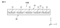
- a wiring board 100B according to a third embodiment will be described with reference to Fig. 9 and Fig. 10.
- Fig. 9 is a plan view of the wiring board according to the third embodiment.
- Fig. 10 is a cross-sectional view taken along line X-X in Fig. 9.
- the wiring board 100B according to the third embodiment differs from the wiring board 100 according to the first embodiment in that an insulating layer 40 is provided.
- At least a portion of the first wiring 31 arranged on the first main surface 11 of the first substrate 10 is covered with an insulating layer 40.
- the first main surface 11 located between two adjacent first wirings 31 is also covered with the insulating layer 40.
- the insulating layer 40 When viewed from the thickness direction (Z direction) of the first substrate, the insulating layer 40 may extend along the X direction.
- the thickness of the insulating layer 40 is not particularly limited, but in order to suppress moisture penetration and achieve a thin structure, the thickness of the insulating layer 40 is preferably 40 ⁇ m or more and 80 ⁇ m or less.
- the material of the insulating layer 40 may be an insulating material based on acrylic oligomer or urethane acrylate.
- the insulating layer 40 is preferably a low water-absorbent insulating resin such as silicone resin, acrylic resin, olefin resin, modified urethane resin, vinyl chloride resin, polyester, polyamide, polyolefin, polyethylene, or polypropylene, or a low water-absorbent insulating layer containing a paraxylylene-based polymer.
- the insulating layer 40 is in the form of a sheet or film.
- a wiring board 100C according to a fourth embodiment will be described with reference to Fig. 11.
- Fig. 11 is a cross-sectional view of the wiring board according to the fourth embodiment.
- Fig. 11 corresponds to Fig. 10 of the third embodiment.
- the wiring board 100C according to the fourth embodiment differs from the wiring board 100 according to the first embodiment in that a covering layer 60 is provided.
- the first wiring 31 is covered with a coating layer 60.
- the first main surface 11 located between two adjacent first wirings 31 is also covered with the coating layer 60. This makes it possible to prevent moisture from entering the first wiring 31 from the outside.
- the coating layer 60 extends along the X direction.
- the thickness of the coating layer 60 is preferably 40 ⁇ m or more and 80 ⁇ m or less.
- the material of the covering layer 60 is not particularly limited, and may be, for example, a laminate.
- the laminate material may be, for example, an adhesive-type stretchable film, a highly adhesive crystal gel, or an ultra-thin PDMS sheet.
- Such a material improves the biocompatibility of the wiring board.
- the covering layer 60 has an affinity for living tissue, which reduces the possibility of the living body having a foreign body reaction or rejection reaction.
- the covering layer 60 is in the form of a film or sheet.
- FIG. 12 is a cross-sectional view of the wiring board according to the fifth embodiment.
- Fig. 12 corresponds to Fig. 10 of the third embodiment.
- the wiring board 100D according to the fifth embodiment is different from the wiring board 100 according to the first embodiment in that a thermoplastic sheet 50 is provided.
- the first wiring 31 is covered with a thermoplastic sheet 50, which contacts and adheres to the first main surface 11.
- the first main surface 11 located between adjacent first wirings 31 is also covered with the thermoplastic sheet 50. This prevents moisture from penetrating into the first wiring 31.
- the connection strength between the thermoplastic sheet 50 and the first wiring 31 is improved, allowing the first wiring 31 to be firmly fixed to the first substrate 10.
- the thermoplastic sheet 50 can be made of a material such as a thermoplastic resin. More specifically, it can be made of a thermoplastic polyurethane (TPU), a polyethylene (PE), or the like.
- the thermoplastic sheet 50 is in the form of a sheet or film. From the viewpoint of making the wiring board thinner overall, it is preferable that the thickness of the thermoplastic sheet 50 is 160 ⁇ m or less.
- the materials of the thermoplastic sheet 50 and the first substrate 10 may be the same or different.
- thermoplastic sheet 50A covers the first wiring 31, contacts and adheres to the first main surface 11, and further contacts and adheres to the second wiring 32. This increases the connection strength between the thermoplastic sheet 50A and the second wiring 32.
- thermoplastic sheet 50A may be spaced apart from the second wiring 32.
- a gap may be provided between the thermoplastic sheet 50A and the second wiring 32. More specifically, in the area where the first substrate 10 and the second substrate 20 overlap, the edge of the thermoplastic sheet 50A and the edge of the second wiring 32 may be spaced apart via a gap.
- thermoplastic sheet 50A being provided so as to be spaced apart from the connection portion between the first wiring 31 and the second wiring 32.
- an edge 81 in the extension direction of the first substrate 10 is positioned further outward in the extension direction of the first substrate 10 than an edge 82 in the extension direction of the first wiring 31.
- the first substrate 10 has another edge 85 on the opposite side of the extension direction to the edge 81, and the edge 81 is farther away from the other edge 85 than the edge 82. This prevents the first wiring 31 from being exposed from the first substrate 10, and the first substrate 10 can protect the first wiring 31.
- FIG. 14 is a cross-sectional view of a second modified example of the wiring board according to the fifth embodiment.
- the thermoplastic sheet 50B covers the first wiring 31, contacts and adheres to the first main surface 11, and further contacts and adheres to the second wiring 32 and the second base material 20. That is, the thermoplastic sheet 50B is arranged so as to be sandwiched between the first substrate 10 and the second substrate 20, and may be in contact with and adhered to both the first main surface 11 and the second main surface 21. This increases the connection strength between the thermoplastic sheet 50B and the second substrate 20. Furthermore, the adhesive strength between the first substrate 10 and the second substrate 20 may also be improved.
- the thermoplastic sheet 50B may have the same thickness as the second wiring 32. More specifically, the thermoplastic sheet 50B may have the same thickness as the second wiring 32 at least in the region where the first substrate 10 and the second substrate 20 overlap. At this time, the thermoplastic sheet 50B may not be in contact with the second wiring 32.
- the thickness of the thermoplastic sheet may be smaller than that of the second wiring 32 as shown in FIG. 13, or may be equal to that of the second wiring 32 as shown in FIG. 14. Alternatively, in order to place more importance on protecting the wiring, the thermoplastic sheet may have a thickness larger than that of the second wiring 32.
- the thickness of the thermoplastic sheet does not necessarily have to be uniform across the X direction.
- the thermoplastic sheet may have a smaller thickness in the region where the first substrate 10 and the second substrate 20 overlap than in other regions. More specifically, the thermoplastic sheet may have a smaller thickness in a portion proximal to the connection point between the first wiring 31 and the second wiring 32. That is, the thermoplastic sheet may have a smaller thickness in the region where multiple components are overlapped. This makes it possible to reduce the overall thickness of the wiring board in the region where multiple components are overlapped, thereby making it possible to make the wiring board thinner.
- thermoplastic sheet as described above may also be provided on the second substrate 20 that is overlaid on the first substrate 10. That is, the second substrate may include a thermoplastic sheet that covers the second wiring 32 and is in contact with and adhered to the second main surface 21. The thermoplastic sheet that covers the second wiring 32 may be in contact with and adhered to the first wiring 31. Alternatively, the thermoplastic sheet that covers the second wiring 32 may be separated from the first wiring 31. By covering each of the first wiring 31 and the second wiring 32 with a thermoplastic sheet, it is possible to obtain the effects of suppressing the intrusion of moisture into each wiring and improving the adhesive strength between the wiring and the base material.
- a wiring having a portion covered by a covering member such as the above-mentioned thermoplastic sheet, insulating layer, and/or covering layer does not necessarily have to have a uniform thickness.
- the overlapping portion of the wiring that overlaps with the covering member and the non-overlapping portion that does not overlap with the covering member may have different thicknesses.
- Such "overlapping portion” and “non-overlapping portion” can also be referred to as “covered portion” and “non-covered portion”, respectively.
- the wiring may have a smaller thickness in the overlapping portion than in the non-overlapping portion.
- the thickness of the wiring in the non-overlapping portion may be larger than the thickness of the wiring in the overlapping portion.
- the wiring is suitably protected by the covering member and can be more suitably adhered to the substrate, so that it is possible for the wiring to have a relatively small thickness. Having a small thickness of the wiring allows the wiring board to be made thinner.
- a wiring board 100E according to a sixth embodiment will be described with reference to Fig. 15.
- Fig. 15 is a cross-sectional view of the wiring board according to the sixth embodiment.
- the wiring board 100E according to the sixth embodiment is different from the wiring board 100B according to the third embodiment in that a covering layer 60 is further provided.
- the insulating layer 40 is covered with a covering layer 60.
- the material of the covering layer 60 is different from that of the insulating layer 40.
- the covering layer 60 extends along the X direction.
- the covering layer 60 is bonded to the insulating layer 40 via an adhesive.
- the covering layer 60 may also be bonded to the second substrate 20.
- the covering layer 60 may be, for example, a laminate.
- the material of the covering layer 60 is, for example, a hydrocarbon-based material, a urethane gel tape, a silicone elastomer, or the like. Such a material improves the biocompatibility of the wiring board.
- the covering layer 60 has an affinity for living tissue, and this can suppress the occurrence of a foreign body reaction or rejection reaction in the living body.
- the thickness of the covering layer 60 is preferably 20 ⁇ m or more and 80 ⁇ m or less.
- a wiring board 100F according to a seventh embodiment will be described with reference to Fig. 16 and Fig. 17.
- Fig. 16 is a plan view of the wiring board according to the seventh embodiment.
- Fig. 17 is a cross-sectional view taken along line XVII-XVII of Fig. 16.
- the wiring board 100F according to the seventh embodiment differs from the wiring board 100E according to the sixth embodiment in that an electronic component 90 and a resist 80 are provided.
- the resist 80 is disposed between the first substrate 10 and the second substrate 20 in the thickness direction (Z direction) of the first substrate. Specifically, the resist 80 is in contact with the first main surface 11 and the second main surface 21. Furthermore, the resist 80 is not present between the first main surface 11 and the first wiring 31, and the resist 80 is not present between the second main surface 21 and the second wiring 32.
- the resist may be disposed so as to be in contact with both the second wiring 32 disposed on the second main surface 21 and the first main surface 11. This allows the space between the first substrate 10 and the second substrate 20 to be filled with the resist 80, thereby preventing foreign matter from adhering to the first wiring 31 from the outside.
- the material of the resist 80 is not particularly limited, but may be, for example, a liquid epoxy solder resist, an alkaline development type solder resist, a UV curing type solder resist, or a heat curing type solder resist.
- the shape of the resist 80 is not particularly limited, but may be a film or sheet.
- the electronic component 90 is electrically connected to the second wiring 32.
- the electronic component 90 may be connected to one or more second wirings 32.
- the type of electronic component 90 but it may be, for example, an inductor or a capacitor.
- the number of electronic components 90 A large number of electronic components 90 may be mounted as necessary.
- a wiring board 100G according to an eighth embodiment will be described with reference to Fig. 18.
- Fig. 18 is a cross-sectional view of the wiring board according to the eighth embodiment.
- Fig. 18 corresponds to Fig. 4 of the first embodiment.
- the wiring board 100G according to the eighth embodiment is different from the wiring board 100 according to the first embodiment in the width of the first wiring 31A.
- the first wiring 31A and the second wiring 32 are in contact.
- the width L3 of the first wiring 31A is smaller than the width L1 of the second wiring 32. This increases the contact area between the first substrate 10 and the second wiring 32, improving the connection strength between the first substrate 10 and the second wiring 32.
- the width L3 of the first wiring 31A is the size in the direction perpendicular to the extension direction of the first wiring 31A when viewed from the Z direction.
- the width L3 of the first wiring 31A is the size of the first wiring 31A in the Y direction.
- the width L3 of the first wiring 31A is the maximum value of the width of the first wiring 31A. If it is difficult to measure the maximum value of the first wiring 31A, the average width of the first wiring 31A is taken as L3.
- the width L1 of the second wiring 32 is the size in the direction perpendicular to the extension direction of the second wiring 32 when viewed from the Z direction.
- the width L1 of the second wiring 32 is the size of the second wiring 32 in the Y direction.
- the width L1 of the second wiring 32 is the maximum width of the second wiring 32. If it is difficult to measure the maximum width of the second wiring 32, the average width of the second wiring 32 is taken as L1.
- the average value refers to the average value of the measurement values obtained by measuring the width of one first wiring 31A at three different points along the extension direction (X direction) in the area where the first substrate 10 and the second substrate 20 overlap.
- a wiring board 100H according to a ninth embodiment will be described with reference to Fig. 19.
- Fig. 19 is a cross-sectional view of the wiring board according to the ninth embodiment.
- Fig. 19 corresponds to Fig. 4 of the first embodiment.
- the wiring board 100H according to the ninth embodiment is different from the wiring board 100 according to the first embodiment in the shape of the third main surface 12.
- the first substrate 10 is in contact with and adhered to the second substrate 20.
- the first substrate 10 covers the first wiring 31 and the second wiring 32.
- the third main surface 12 of the first substrate 10, which is located on the opposite side of the first main surface in contact with the first wiring 31, has an uneven shape. This increases the surface area of the third main surface 12 of the first substrate 10, improving the heat dissipation of the first wiring 31.
- the heater comes into contact with the convex parts of the third main surface 12, and heat can be concentrated on the convex parts of the first substrate 10. This allows for rapid thermocompression bonding.
- the third main surface 12 when viewed from the Z direction, has a convex shape in the region where it overlaps with the first wiring 31, and a concave shape in the region between two adjacent first wirings 31.
- the third main surface 12 is formed along the first wiring 31 and the second main surface 21 between the two adjacent first wirings 31.
- Fig. 20 is a cross-sectional view of the wiring board according to the tenth embodiment.
- Fig. 20 corresponds to Fig. 4 of the first embodiment.
- the wiring board 100I according to the tenth embodiment is different from the wiring board 100 according to the first embodiment in the size and number of second wirings 32A.
- the first wirings 31 and one second wiring 32A are electrically connected to face each other in the thickness direction (Z direction) of the first substrate. That is, among the first wirings 31 arranged on the first main surface 11, at least two first wirings 31 may be electrically connected to the same second wiring 32A. Specifically, the width of the second wiring 32A in the Y direction is larger than the width of the first wiring 31 in the Y direction, and two or more first wirings 31 are connected to one second wiring 32A.
- the second wiring 32A may extend in the Y direction so as to be mutually connected to each of the first wirings 31 arranged in parallel with each other in the Y direction.
- the adjacent first wirings 31 are spaced apart from each other. This reduces the number of second wirings 32A relative to the first wirings 31, and increases the design freedom of the wiring board 100I.
- a portion of the first substrate 10 is disposed between each of the multiple adjacent first wirings 31 and contacts the second wiring 32A. This ensures insulation between the adjacent first wirings 31.
- the form of connection between the first wiring 31 and the second wiring 32A is not particularly limited. For example, multiple second wirings and one first wiring may be electrically connected. In this case, it is preferable that the second substrate 20 is made of the same material as the first substrate 10.
Landscapes
- Engineering & Computer Science (AREA)
- Microelectronics & Electronic Packaging (AREA)
- Structure Of Printed Boards (AREA)
Priority Applications (2)
| Application Number | Priority Date | Filing Date | Title |
|---|---|---|---|
| JP2024549941A JP7747227B2 (ja) | 2022-09-30 | 2023-09-04 | 配線基板 |
| US19/089,550 US20250227846A1 (en) | 2022-09-30 | 2025-03-25 | Wiring board |
Applications Claiming Priority (2)
| Application Number | Priority Date | Filing Date | Title |
|---|---|---|---|
| US202263411770P | 2022-09-30 | 2022-09-30 | |
| US63/411,770 | 2022-09-30 |
Related Child Applications (1)
| Application Number | Title | Priority Date | Filing Date |
|---|---|---|---|
| US19/089,550 Continuation US20250227846A1 (en) | 2022-09-30 | 2025-03-25 | Wiring board |
Publications (1)
| Publication Number | Publication Date |
|---|---|
| WO2024070518A1 true WO2024070518A1 (ja) | 2024-04-04 |
Family
ID=90477330
Family Applications (1)
| Application Number | Title | Priority Date | Filing Date |
|---|---|---|---|
| PCT/JP2023/032240 Ceased WO2024070518A1 (ja) | 2022-09-30 | 2023-09-04 | 配線基板 |
Country Status (3)
| Country | Link |
|---|---|
| US (1) | US20250227846A1 (https=) |
| JP (1) | JP7747227B2 (https=) |
| WO (1) | WO2024070518A1 (https=) |
Citations (9)
| Publication number | Priority date | Publication date | Assignee | Title |
|---|---|---|---|---|
| JP2000049423A (ja) * | 1998-07-30 | 2000-02-18 | Sony Chem Corp | フレキシブル基板 |
| JP2001111209A (ja) * | 1999-07-30 | 2001-04-20 | Denso Corp | プリント配線板の接続方法および接続構造 |
| JP2001223465A (ja) * | 1999-11-30 | 2001-08-17 | Denso Corp | プリント配線基板の接続方法及び接続構造 |
| JP2002050863A (ja) * | 2000-08-04 | 2002-02-15 | Denso Corp | プリント配線基板の接続方法 |
| JP2004247403A (ja) * | 2003-02-12 | 2004-09-02 | Denso Wave Inc | 半田付け装置、半田付け方法、基板接続装置及び基板接続方法 |
| JP2004311578A (ja) * | 2003-04-03 | 2004-11-04 | Fujikura Ltd | プリント配線基板の接合方法並びに複合プリント配線基板 |
| JP2005045066A (ja) * | 2003-07-23 | 2005-02-17 | Matsushita Electric Ind Co Ltd | 電気的接続構造およびその製造方法 |
| JP2015023059A (ja) * | 2013-07-16 | 2015-02-02 | 住友電工プリントサーキット株式会社 | フレキシブルプリント配線板の接続構造、フレキシブルプリント配線板及びその製造方法 |
| JP2017195230A (ja) * | 2016-04-18 | 2017-10-26 | 日本メクトロン株式会社 | 伸縮性配線基板、及び、伸縮性配線基板の製造方法 |
-
2023
- 2023-09-04 JP JP2024549941A patent/JP7747227B2/ja active Active
- 2023-09-04 WO PCT/JP2023/032240 patent/WO2024070518A1/ja not_active Ceased
-
2025
- 2025-03-25 US US19/089,550 patent/US20250227846A1/en active Pending
Patent Citations (9)
| Publication number | Priority date | Publication date | Assignee | Title |
|---|---|---|---|---|
| JP2000049423A (ja) * | 1998-07-30 | 2000-02-18 | Sony Chem Corp | フレキシブル基板 |
| JP2001111209A (ja) * | 1999-07-30 | 2001-04-20 | Denso Corp | プリント配線板の接続方法および接続構造 |
| JP2001223465A (ja) * | 1999-11-30 | 2001-08-17 | Denso Corp | プリント配線基板の接続方法及び接続構造 |
| JP2002050863A (ja) * | 2000-08-04 | 2002-02-15 | Denso Corp | プリント配線基板の接続方法 |
| JP2004247403A (ja) * | 2003-02-12 | 2004-09-02 | Denso Wave Inc | 半田付け装置、半田付け方法、基板接続装置及び基板接続方法 |
| JP2004311578A (ja) * | 2003-04-03 | 2004-11-04 | Fujikura Ltd | プリント配線基板の接合方法並びに複合プリント配線基板 |
| JP2005045066A (ja) * | 2003-07-23 | 2005-02-17 | Matsushita Electric Ind Co Ltd | 電気的接続構造およびその製造方法 |
| JP2015023059A (ja) * | 2013-07-16 | 2015-02-02 | 住友電工プリントサーキット株式会社 | フレキシブルプリント配線板の接続構造、フレキシブルプリント配線板及びその製造方法 |
| JP2017195230A (ja) * | 2016-04-18 | 2017-10-26 | 日本メクトロン株式会社 | 伸縮性配線基板、及び、伸縮性配線基板の製造方法 |
Also Published As
| Publication number | Publication date |
|---|---|
| JPWO2024070518A1 (https=) | 2024-04-04 |
| JP7747227B2 (ja) | 2025-10-01 |
| US20250227846A1 (en) | 2025-07-10 |
Similar Documents
| Publication | Publication Date | Title |
|---|---|---|
| US20220377886A1 (en) | Laminated body and method for manufacturing the same | |
| US10847695B2 (en) | Light emitting device | |
| JP2009038139A (ja) | 半導体装置およびその製造方法 | |
| US11622442B2 (en) | Circuit member joint structure and circuit member joining method | |
| JP5672091B2 (ja) | 多層基板 | |
| JP7747227B2 (ja) | 配線基板 | |
| JP2013135172A (ja) | プリント配線板及びプリント配線板の接続構造 | |
| US20250210505A1 (en) | Stretchable device | |
| JP6683264B2 (ja) | 電子機器 | |
| US20170090108A1 (en) | Planar illumination device | |
| US12451268B2 (en) | Electric contact terminal | |
| TWI855712B (zh) | 顯示裝置 | |
| WO2023171464A1 (ja) | 伸縮性デバイス | |
| JP5006162B2 (ja) | 電気接続部材 | |
| WO2024070591A1 (ja) | 伸縮性デバイス | |
| JP7036213B2 (ja) | フレキシブル基板及びその製造方法、並びに電子機器 | |
| US12349596B2 (en) | Vibration device | |
| US20230050989A1 (en) | Signal transmission line | |
| JP6460280B2 (ja) | 部品実装基板 | |
| WO2025033274A1 (ja) | 伸縮性デバイス | |
| JP4085609B2 (ja) | 端子付き配線基板 | |
| WO2024122492A1 (ja) | 半導体装置 | |
| WO2025249367A1 (ja) | 伸縮性デバイス | |
| JP2024007723A (ja) | 圧電振動ユニット | |
| TW202338448A (zh) | 電子裝置 |
Legal Events
| Date | Code | Title | Description |
|---|---|---|---|
| 121 | Ep: the epo has been informed by wipo that ep was designated in this application |
Ref document number: 23871758 Country of ref document: EP Kind code of ref document: A1 |
|
| WWE | Wipo information: entry into national phase |
Ref document number: 2024549941 Country of ref document: JP |
|
| NENP | Non-entry into the national phase |
Ref country code: DE |
|
| 122 | Ep: pct application non-entry in european phase |
Ref document number: 23871758 Country of ref document: EP Kind code of ref document: A1 |