WO2023214500A1 - 半導体装置 - Google Patents
半導体装置 Download PDFInfo
- Publication number
- WO2023214500A1 WO2023214500A1 PCT/JP2023/015070 JP2023015070W WO2023214500A1 WO 2023214500 A1 WO2023214500 A1 WO 2023214500A1 JP 2023015070 W JP2023015070 W JP 2023015070W WO 2023214500 A1 WO2023214500 A1 WO 2023214500A1
- Authority
- WO
- WIPO (PCT)
- Prior art keywords
- semiconductor device
- resin
- thickness direction
- recess
- terminal
- Prior art date
- Legal status (The legal status is an assumption and is not a legal conclusion. Google has not performed a legal analysis and makes no representation as to the accuracy of the status listed.)
- Ceased
Links
Images


Classifications
-
- H—ELECTRICITY
- H10—SEMICONDUCTOR DEVICES; ELECTRIC SOLID-STATE DEVICES NOT OTHERWISE PROVIDED FOR
- H10W—GENERIC PACKAGES, INTERCONNECTIONS, CONNECTORS OR OTHER CONSTRUCTIONAL DETAILS OF DEVICES COVERED BY CLASS H10
- H10W74/00—Encapsulations, e.g. protective coatings
- H10W74/10—Encapsulations, e.g. protective coatings characterised by their shape or disposition
- H10W74/111—Encapsulations, e.g. protective coatings characterised by their shape or disposition the semiconductor body being completely enclosed
- H10W74/114—Encapsulations, e.g. protective coatings characterised by their shape or disposition the semiconductor body being completely enclosed by a substrate and the encapsulations
-
- H—ELECTRICITY
- H10—SEMICONDUCTOR DEVICES; ELECTRIC SOLID-STATE DEVICES NOT OTHERWISE PROVIDED FOR
- H10D—INORGANIC ELECTRIC SEMICONDUCTOR DEVICES
- H10D80/00—Assemblies of multiple devices comprising at least one device covered by this subclass
- H10D80/20—Assemblies of multiple devices comprising at least one device covered by this subclass the at least one device being covered by groups H10D1/00 - H10D48/00, e.g. assemblies comprising capacitors, power FETs or Schottky diodes
- H10D80/251—FETs covered by H10D30/00, e.g. power FETs
-
- H—ELECTRICITY
- H10—SEMICONDUCTOR DEVICES; ELECTRIC SOLID-STATE DEVICES NOT OTHERWISE PROVIDED FOR
- H10W—GENERIC PACKAGES, INTERCONNECTIONS, CONNECTORS OR OTHER CONSTRUCTIONAL DETAILS OF DEVICES COVERED BY CLASS H10
- H10W40/00—Arrangements for thermal protection or thermal control
- H10W40/20—Arrangements for cooling
- H10W40/25—Arrangements for cooling characterised by their materials
- H10W40/255—Arrangements for cooling characterised by their materials having a laminate or multilayered structure, e.g. direct bond copper [DBC] ceramic substrates
-
- H—ELECTRICITY
- H10—SEMICONDUCTOR DEVICES; ELECTRIC SOLID-STATE DEVICES NOT OTHERWISE PROVIDED FOR
- H10D—INORGANIC ELECTRIC SEMICONDUCTOR DEVICES
- H10D80/00—Assemblies of multiple devices comprising at least one device covered by this subclass
- H10D80/20—Assemblies of multiple devices comprising at least one device covered by this subclass the at least one device being covered by groups H10D1/00 - H10D48/00, e.g. assemblies comprising capacitors, power FETs or Schottky diodes
-
- H—ELECTRICITY
- H10—SEMICONDUCTOR DEVICES; ELECTRIC SOLID-STATE DEVICES NOT OTHERWISE PROVIDED FOR
- H10W—GENERIC PACKAGES, INTERCONNECTIONS, CONNECTORS OR OTHER CONSTRUCTIONAL DETAILS OF DEVICES COVERED BY CLASS H10
- H10W70/00—Package substrates; Interposers; Redistribution layers [RDL]
- H10W70/40—Leadframes
- H10W70/411—Chip-supporting parts, e.g. die pads
- H10W70/413—Insulating or insulated substrates serving as die pads
-
- H—ELECTRICITY
- H10—SEMICONDUCTOR DEVICES; ELECTRIC SOLID-STATE DEVICES NOT OTHERWISE PROVIDED FOR
- H10W—GENERIC PACKAGES, INTERCONNECTIONS, CONNECTORS OR OTHER CONSTRUCTIONAL DETAILS OF DEVICES COVERED BY CLASS H10
- H10W70/00—Package substrates; Interposers; Redistribution layers [RDL]
- H10W70/40—Leadframes
- H10W70/464—Additional interconnections in combination with leadframes
- H10W70/468—Circuit boards
-
- H—ELECTRICITY
- H10—SEMICONDUCTOR DEVICES; ELECTRIC SOLID-STATE DEVICES NOT OTHERWISE PROVIDED FOR
- H10W—GENERIC PACKAGES, INTERCONNECTIONS, CONNECTORS OR OTHER CONSTRUCTIONAL DETAILS OF DEVICES COVERED BY CLASS H10
- H10W70/00—Package substrates; Interposers; Redistribution layers [RDL]
- H10W70/40—Leadframes
- H10W70/481—Leadframes for devices being provided for in groups H10D8/00 - H10D48/00
-
- H—ELECTRICITY
- H10—SEMICONDUCTOR DEVICES; ELECTRIC SOLID-STATE DEVICES NOT OTHERWISE PROVIDED FOR
- H10W—GENERIC PACKAGES, INTERCONNECTIONS, CONNECTORS OR OTHER CONSTRUCTIONAL DETAILS OF DEVICES COVERED BY CLASS H10
- H10W70/00—Package substrates; Interposers; Redistribution layers [RDL]
- H10W70/60—Insulating or insulated package substrates; Interposers; Redistribution layers
- H10W70/62—Insulating or insulated package substrates; Interposers; Redistribution layers characterised by their interconnections
- H10W70/65—Shapes or dispositions of interconnections
- H10W70/658—Shapes or dispositions of interconnections for devices provided for in groups H10D8/00 - H10D48/00
-
- H—ELECTRICITY
- H10—SEMICONDUCTOR DEVICES; ELECTRIC SOLID-STATE DEVICES NOT OTHERWISE PROVIDED FOR
- H10W—GENERIC PACKAGES, INTERCONNECTIONS, CONNECTORS OR OTHER CONSTRUCTIONAL DETAILS OF DEVICES COVERED BY CLASS H10
- H10W74/00—Encapsulations, e.g. protective coatings
- H10W74/10—Encapsulations, e.g. protective coatings characterised by their shape or disposition
- H10W74/111—Encapsulations, e.g. protective coatings characterised by their shape or disposition the semiconductor body being completely enclosed
-
- H—ELECTRICITY
- H10—SEMICONDUCTOR DEVICES; ELECTRIC SOLID-STATE DEVICES NOT OTHERWISE PROVIDED FOR
- H10W—GENERIC PACKAGES, INTERCONNECTIONS, CONNECTORS OR OTHER CONSTRUCTIONAL DETAILS OF DEVICES COVERED BY CLASS H10
- H10W90/00—Package configurations
- H10W90/10—Configurations of laterally-adjacent chips
-
- H—ELECTRICITY
- H10—SEMICONDUCTOR DEVICES; ELECTRIC SOLID-STATE DEVICES NOT OTHERWISE PROVIDED FOR
- H10W—GENERIC PACKAGES, INTERCONNECTIONS, CONNECTORS OR OTHER CONSTRUCTIONAL DETAILS OF DEVICES COVERED BY CLASS H10
- H10W90/00—Package configurations
- H10W90/701—Package configurations characterised by the relative positions of pads or connectors relative to package parts
- H10W90/761—Package configurations characterised by the relative positions of pads or connectors relative to package parts of strap connectors
- H10W90/763—Package configurations characterised by the relative positions of pads or connectors relative to package parts of strap connectors between laterally-adjacent chips
-
- H—ELECTRICITY
- H10—SEMICONDUCTOR DEVICES; ELECTRIC SOLID-STATE DEVICES NOT OTHERWISE PROVIDED FOR
- H10W—GENERIC PACKAGES, INTERCONNECTIONS, CONNECTORS OR OTHER CONSTRUCTIONAL DETAILS OF DEVICES COVERED BY CLASS H10
- H10W70/00—Package substrates; Interposers; Redistribution layers [RDL]
- H10W70/40—Leadframes
- H10W70/421—Shapes or dispositions
-
- H—ELECTRICITY
- H10—SEMICONDUCTOR DEVICES; ELECTRIC SOLID-STATE DEVICES NOT OTHERWISE PROVIDED FOR
- H10W—GENERIC PACKAGES, INTERCONNECTIONS, CONNECTORS OR OTHER CONSTRUCTIONAL DETAILS OF DEVICES COVERED BY CLASS H10
- H10W70/00—Package substrates; Interposers; Redistribution layers [RDL]
- H10W70/40—Leadframes
- H10W70/464—Additional interconnections in combination with leadframes
- H10W70/467—Multilayered additional interconnections
-
- H—ELECTRICITY
- H10—SEMICONDUCTOR DEVICES; ELECTRIC SOLID-STATE DEVICES NOT OTHERWISE PROVIDED FOR
- H10W—GENERIC PACKAGES, INTERCONNECTIONS, CONNECTORS OR OTHER CONSTRUCTIONAL DETAILS OF DEVICES COVERED BY CLASS H10
- H10W72/00—Interconnections or connectors in packages
- H10W72/851—Dispositions of multiple connectors or interconnections
- H10W72/853—On the same surface
- H10W72/871—Bond wires and strap connectors
-
- H—ELECTRICITY
- H10—SEMICONDUCTOR DEVICES; ELECTRIC SOLID-STATE DEVICES NOT OTHERWISE PROVIDED FOR
- H10W—GENERIC PACKAGES, INTERCONNECTIONS, CONNECTORS OR OTHER CONSTRUCTIONAL DETAILS OF DEVICES COVERED BY CLASS H10
- H10W72/00—Interconnections or connectors in packages
- H10W72/851—Dispositions of multiple connectors or interconnections
- H10W72/874—On different surfaces
- H10W72/884—Die-attach connectors and bond wires
-
- H—ELECTRICITY
- H10—SEMICONDUCTOR DEVICES; ELECTRIC SOLID-STATE DEVICES NOT OTHERWISE PROVIDED FOR
- H10W—GENERIC PACKAGES, INTERCONNECTIONS, CONNECTORS OR OTHER CONSTRUCTIONAL DETAILS OF DEVICES COVERED BY CLASS H10
- H10W72/00—Interconnections or connectors in packages
- H10W72/851—Dispositions of multiple connectors or interconnections
- H10W72/874—On different surfaces
- H10W72/886—Die-attach connectors and strap connectors
-
- H—ELECTRICITY
- H10—SEMICONDUCTOR DEVICES; ELECTRIC SOLID-STATE DEVICES NOT OTHERWISE PROVIDED FOR
- H10W—GENERIC PACKAGES, INTERCONNECTIONS, CONNECTORS OR OTHER CONSTRUCTIONAL DETAILS OF DEVICES COVERED BY CLASS H10
- H10W74/00—Encapsulations, e.g. protective coatings
- H10W74/10—Encapsulations, e.g. protective coatings characterised by their shape or disposition
-
- H—ELECTRICITY
- H10—SEMICONDUCTOR DEVICES; ELECTRIC SOLID-STATE DEVICES NOT OTHERWISE PROVIDED FOR
- H10W—GENERIC PACKAGES, INTERCONNECTIONS, CONNECTORS OR OTHER CONSTRUCTIONAL DETAILS OF DEVICES COVERED BY CLASS H10
- H10W90/00—Package configurations
-
- H—ELECTRICITY
- H10—SEMICONDUCTOR DEVICES; ELECTRIC SOLID-STATE DEVICES NOT OTHERWISE PROVIDED FOR
- H10W—GENERIC PACKAGES, INTERCONNECTIONS, CONNECTORS OR OTHER CONSTRUCTIONAL DETAILS OF DEVICES COVERED BY CLASS H10
- H10W90/00—Package configurations
- H10W90/701—Package configurations characterised by the relative positions of pads or connectors relative to package parts
- H10W90/731—Package configurations characterised by the relative positions of pads or connectors relative to package parts of die-attach connectors
- H10W90/734—Package configurations characterised by the relative positions of pads or connectors relative to package parts of die-attach connectors between a chip and a stacked insulating package substrate, interposer or RDL
-
- H—ELECTRICITY
- H10—SEMICONDUCTOR DEVICES; ELECTRIC SOLID-STATE DEVICES NOT OTHERWISE PROVIDED FOR
- H10W—GENERIC PACKAGES, INTERCONNECTIONS, CONNECTORS OR OTHER CONSTRUCTIONAL DETAILS OF DEVICES COVERED BY CLASS H10
- H10W90/00—Package configurations
- H10W90/701—Package configurations characterised by the relative positions of pads or connectors relative to package parts
- H10W90/751—Package configurations characterised by the relative positions of pads or connectors relative to package parts of bond wires
- H10W90/754—Package configurations characterised by the relative positions of pads or connectors relative to package parts of bond wires between a chip and a stacked insulating package substrate, interposer or RDL
-
- H—ELECTRICITY
- H10—SEMICONDUCTOR DEVICES; ELECTRIC SOLID-STATE DEVICES NOT OTHERWISE PROVIDED FOR
- H10W—GENERIC PACKAGES, INTERCONNECTIONS, CONNECTORS OR OTHER CONSTRUCTIONAL DETAILS OF DEVICES COVERED BY CLASS H10
- H10W90/00—Package configurations
- H10W90/701—Package configurations characterised by the relative positions of pads or connectors relative to package parts
- H10W90/751—Package configurations characterised by the relative positions of pads or connectors relative to package parts of bond wires
- H10W90/756—Package configurations characterised by the relative positions of pads or connectors relative to package parts of bond wires between a chip and a stacked lead frame, conducting package substrate or heat sink
-
- H—ELECTRICITY
- H10—SEMICONDUCTOR DEVICES; ELECTRIC SOLID-STATE DEVICES NOT OTHERWISE PROVIDED FOR
- H10W—GENERIC PACKAGES, INTERCONNECTIONS, CONNECTORS OR OTHER CONSTRUCTIONAL DETAILS OF DEVICES COVERED BY CLASS H10
- H10W90/00—Package configurations
- H10W90/701—Package configurations characterised by the relative positions of pads or connectors relative to package parts
- H10W90/761—Package configurations characterised by the relative positions of pads or connectors relative to package parts of strap connectors
- H10W90/764—Package configurations characterised by the relative positions of pads or connectors relative to package parts of strap connectors between a chip and a stacked insulating package substrate, interposer or RDL
-
- H—ELECTRICITY
- H10—SEMICONDUCTOR DEVICES; ELECTRIC SOLID-STATE DEVICES NOT OTHERWISE PROVIDED FOR
- H10W—GENERIC PACKAGES, INTERCONNECTIONS, CONNECTORS OR OTHER CONSTRUCTIONAL DETAILS OF DEVICES COVERED BY CLASS H10
- H10W90/00—Package configurations
- H10W90/811—Multiple chips on leadframes
Definitions
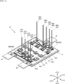
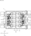
- the first control terminal 46E is a drain signal detection terminal (drain sense terminal) of the plurality of first semiconductor elements 10A.
- the voltage (voltage corresponding to the drain current) applied to each back electrode 15 (drain electrode) of the plurality of first semiconductor elements 10A is detected from the first control terminal 46E.
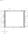
- the semiconductor device B1 converts the DC power supply voltage applied to the first power terminal 14 and the two second power terminals 15 into AC power using the plurality of semiconductor elements 21.
- the converted AC power is input from the two third power terminals 16 to a power supply target such as a motor.
- the two second power terminals 15 are separated from the first conductive part 1121 and the second conductive part 1122, respectively.
- the two second power terminals 15 each extend in the first direction x, and protrude from the sealing resin 50 in the x1 side of the first direction x.
- each of the two second power terminals 15 includes a portion covered with the sealing resin 50 and a portion exposed from the sealing resin 50.
- a second conductive member 32 is joined to a portion of each second power terminal 15 covered with the sealing resin 50 . Further, in each second power terminal 15, the portion exposed from the sealing resin 50 is used as the above-mentioned N terminal of the semiconductor device B1.
- each of the two third power terminals 16 includes a portion covered with the sealing resin 50 and a portion exposed from the sealing resin 50.
- a portion covered with the sealing resin 50 is joined to the second conductive portion 1122. Further, in each third power terminal 16, the portion exposed from the sealing resin 50 is used as the above-mentioned output terminal of the semiconductor device B1.
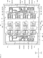
- the first control terminal 46B is a terminal (source sense terminal) for detecting source signals of the plurality of first elements 21A.
- the voltage (voltage corresponding to the source current) applied to each second electrode 212 (source electrode) of the plurality of first elements 21A is detected from the first control terminal 46B.
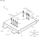
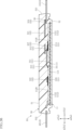
- the first flange portion 454 is connected to the end portion of the cylindrical portion 453 on the z1 side in the thickness direction z.
- the first flange portion 454 has a first surface 454a.
- the first surface 454a is a surface facing the z1 side in the thickness direction z.
- the first surface 454a is located at the end of the holder 451 on the z1 side in the thickness direction z.
- the first surface 454a has an annular shape (an annular shape in the illustrated example) when viewed in the thickness direction z.
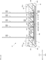
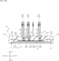
- FIG. 45 shows one step in the manufacturing process of the semiconductor device B1, and is a cross-sectional view similar to FIG. 44.
- a mold 91 for molding is provided with a cylindrical pin 911.
- the holder 451 is placed in the inner space of the cylindrical pin 911, and the mold is pressed while pressing the lower end of the cylindrical pin 911 (the end on the z2 side in the thickness direction z) against the control terminal support 48 (first metal layer 482).
- a fluid resin material is injected into the cavity space 919 of 91 .
- each first recess 511 is filled with a first resin portion 55.
- the first resin portion 55 covers the holder 451 disposed in each first recess 511.
- the elastic modulus of the first resin portion 55 is smaller than the elastic modulus of the sealing resin 50. According to such a configuration, stress around the holder 451 covered by the first resin portion 55 can be reduced. Further, in the semiconductor device B12, by providing the first resin portion 55, it is possible to prevent foreign matter (including moisture) from entering the first recessed portion 511 exposed from the sealing resin 50.
- the semiconductor device B12 having the above configuration is preferable in terms of improving durability and reliability.
- the semiconductor device B12 has the same functions and effects as the semiconductor device B1 of the above embodiment within the same configuration range as the semiconductor device B1 of the above embodiment.
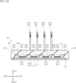
- FIG. 50 shows a semiconductor device according to a third modification of the first embodiment on the second side.
- FIG. 50 is a cross-sectional view showing the semiconductor device B13 of this modification, and is a cross-sectional view similar to FIG. 47.
- the semiconductor device B13 of this modification further includes a first resin portion 55, and differs from the semiconductor device B11 of the modification in that it includes the first resin portion 55.
- the first resin portion 55 fills at least a portion of the first recess 511 and contacts at least a portion of the holder 451. In the semiconductor device B13, the first resin portion 55 partially fills the first recess 511.
- the first resin part 55 covers a part of each of the plurality of holders 451 arranged in the first recess 511.
- the constituent material of the first resin portion 55 is not particularly limited.
- the first resin portion 55 may be made of the same material as the sealing resin 50, or may be made of a different material from the sealing resin 50. In the semiconductor device B13, for example, the constituent material of the first resin portion 55 is different from the constituent material of the sealing resin 50.
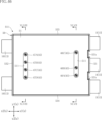
- the first resin portion 55 fills at least a portion of the first recess 511 and contacts at least a portion of the holder 451. In the semiconductor device B ⁇ b>14 , the first resin portion 55 is filled in each first recess 511 so as to fill each first recess 511 .
- the constituent material of the first resin portion 55 is not particularly limited.
- the first resin portion 55 may be made of the same material as the sealing resin 50, or may be made of a different material from the sealing resin 50. In the semiconductor device B14, for example, the constituent material of the first resin portion 55 is different from the constituent material of the sealing resin 50. In the semiconductor device B14, for example, the elastic modulus of the first resin portion 55 is smaller than the elastic modulus of the sealing resin 50. In this way, when the elastic modulus of the first resin part 55 is smaller than that of the sealing resin 50, the constituent material of the first resin part 55 is not particularly limited, and examples thereof include silicone resin, silicone gel, etc. .
- each control terminal 45 is entirely exposed from the sealing resin 50. According to such a configuration, it is possible to prevent the sealing resin 50 from flowing into the inside of the holder 451 into which the metal pin 452 is inserted. Therefore, in the semiconductor device B14, conduction between the holder 451 and the metal pins 452 can be maintained appropriately, and the control terminal 45 including the holder 451 and the metal pins 452 can function appropriately.
Landscapes
- Structures Or Materials For Encapsulating Or Coating Semiconductor Devices Or Solid State Devices (AREA)
- Lead Frames For Integrated Circuits (AREA)
- Engineering & Computer Science (AREA)
- Microelectronics & Electronic Packaging (AREA)
- Cooling Or The Like Of Semiconductors Or Solid State Devices (AREA)
Priority Applications (14)
| Application Number | Priority Date | Filing Date | Title |
|---|---|---|---|
| JP2024519184A JP7820505B2 (ja) | 2022-05-02 | 2023-04-13 | 半導体装置 |
| EP23799432.2A EP4517823A4 (en) | 2022-05-02 | 2023-04-13 | SEMICONDUCTOR DEVICE |
| CN202511987189.2A CN121712087A (zh) | 2022-05-02 | 2023-04-13 | 半导体装置 |
| CN202380037337.7A CN119110995A (zh) | 2022-05-02 | 2023-04-13 | 半导体装置 |
| EP26153621.3A EP4707924A3 (en) | 2022-05-02 | 2023-04-13 | Semiconductor device |
| EP25196791.5A EP4629292A3 (en) | 2022-05-02 | 2023-04-13 | Semiconductor device |
| DE112023001614.3T DE112023001614T5 (de) | 2022-05-02 | 2023-04-13 | Halbleitervorrichtung |
| EP26165088.1A EP4739065A2 (en) | 2022-05-02 | 2023-04-13 | Semiconductor device |
| CN202511122387.2A CN120751756B (zh) | 2022-05-02 | 2023-04-13 | 半导体装置 |
| US18/923,061 US20250046664A1 (en) | 2022-05-02 | 2024-10-22 | Semiconductor device |
| JP2025053922A JP7799880B2 (ja) | 2022-05-02 | 2025-03-27 | 半導体装置、および半導体装置の製造方法 |
| JP2025102667A JP7725758B1 (ja) | 2022-05-02 | 2025-06-18 | 半導体装置、および半導体装置の製造方法 |
| JP2025131436A JP2025163208A (ja) | 2022-05-02 | 2025-08-06 | 半導体装置、および半導体装置の製造方法 |
| US19/310,211 US20250379111A1 (en) | 2022-05-02 | 2025-08-26 | Semiconductor device |
Applications Claiming Priority (4)
| Application Number | Priority Date | Filing Date | Title |
|---|---|---|---|
| JP2022075921 | 2022-05-02 | ||
| JP2022-075921 | 2022-05-02 | ||
| JP2022127149 | 2022-08-09 | ||
| JP2022-127149 | 2022-08-09 |
Related Child Applications (1)
| Application Number | Title | Priority Date | Filing Date |
|---|---|---|---|
| US18/923,061 Continuation US20250046664A1 (en) | 2022-05-02 | 2024-10-22 | Semiconductor device |
Publications (1)
| Publication Number | Publication Date |
|---|---|
| WO2023214500A1 true WO2023214500A1 (ja) | 2023-11-09 |
Family
ID=88646429
Family Applications (1)
| Application Number | Title | Priority Date | Filing Date |
|---|---|---|---|
| PCT/JP2023/015070 Ceased WO2023214500A1 (ja) | 2022-05-02 | 2023-04-13 | 半導体装置 |
Country Status (6)
| Country | Link |
|---|---|
| US (2) | US20250046664A1 (https=) |
| EP (4) | EP4629292A3 (https=) |
| JP (4) | JP7820505B2 (https=) |
| CN (3) | CN121712087A (https=) |
| DE (1) | DE112023001614T5 (https=) |
| WO (1) | WO2023214500A1 (https=) |
Cited By (3)
| Publication number | Priority date | Publication date | Assignee | Title |
|---|---|---|---|---|
| US20230154815A1 (en) * | 2020-04-27 | 2023-05-18 | Rohm Co., Ltd. | Semiconductor device |
| WO2025154475A1 (ja) * | 2024-01-18 | 2025-07-24 | ローム株式会社 | 半導体装置および半導体装置の製造方法 |
| JP2025117524A (ja) * | 2024-01-30 | 2025-08-12 | 朋程科技股▲ふん▼有限公司 | 半導体モジュール及びその製造方法 |
Families Citing this family (2)
| Publication number | Priority date | Publication date | Assignee | Title |
|---|---|---|---|---|
| EP4379966A4 (en) * | 2021-07-28 | 2024-09-04 | Mitsubishi Electric Corporation | CIRCUIT CONNECTION DEVICE, DYNAMOELECTRIC MACHINE DEVICE, AND METHOD FOR MANUFACTURING CIRCUIT CONNECTION DEVICE |
| DE102025101191B3 (de) | 2025-01-14 | 2026-03-26 | Volkswagen Aktiengesellschaft | Vorrichtung für einen Stromwandler, Stromwandler und Fahrzeug |
Citations (6)
| Publication number | Priority date | Publication date | Assignee | Title |
|---|---|---|---|---|
| JP2007184315A (ja) * | 2006-01-04 | 2007-07-19 | Hitachi Ltd | 樹脂封止型パワー半導体モジュール |
| JP2011165836A (ja) * | 2010-02-09 | 2011-08-25 | Mitsubishi Electric Corp | 電力用半導体装置 |
| JP2014123618A (ja) * | 2012-12-20 | 2014-07-03 | Mitsubishi Electric Corp | 半導体モジュール、その製造方法およびその接続方法 |
| US20190115275A1 (en) * | 2017-10-13 | 2019-04-18 | Semiconductor Components Industries, Llc | Semiconductor package and related methods |
| JP2021190505A (ja) | 2020-05-27 | 2021-12-13 | ローム株式会社 | 半導体装置 |
| WO2022080063A1 (ja) * | 2020-10-14 | 2022-04-21 | ローム株式会社 | 半導体モジュール |
Family Cites Families (16)
| Publication number | Priority date | Publication date | Assignee | Title |
|---|---|---|---|---|
| JPH04127996U (ja) * | 1991-05-16 | 1992-11-20 | ナイルス部品株式会社 | モジユールにおける端子の接続構造 |
| DE10324139B4 (de) * | 2003-05-26 | 2005-07-21 | Infineon Technologies Ag | Mikroelektromechanisches Bauteil und Verfahren zu seiner Herstellung |
| JP5272768B2 (ja) | 2009-02-05 | 2013-08-28 | 三菱電機株式会社 | 電力用半導体装置とその製造方法 |
| JP5171777B2 (ja) * | 2009-09-30 | 2013-03-27 | 三菱電機株式会社 | 電力用半導体装置 |
| JP5261851B2 (ja) * | 2010-04-08 | 2013-08-14 | 三菱電機株式会社 | 半導体装置の製造方法 |
| JP5383621B2 (ja) | 2010-10-20 | 2014-01-08 | 三菱電機株式会社 | パワー半導体装置 |
| JP5649142B2 (ja) * | 2011-04-05 | 2015-01-07 | パナソニック株式会社 | 封止型半導体装置及びその製造方法 |
| KR102143890B1 (ko) | 2013-10-15 | 2020-08-12 | 온세미컨덕터코리아 주식회사 | 파워 모듈 패키지 및 이의 제조 방법 |
| KR20150060036A (ko) * | 2013-11-25 | 2015-06-03 | 삼성전기주식회사 | 전력 반도체 모듈 및 그 제조 방법 |
| US10153424B2 (en) * | 2016-08-22 | 2018-12-11 | Rohm Co., Ltd. | Semiconductor device and mounting structure of semiconductor device |
| JP2018113326A (ja) * | 2017-01-11 | 2018-07-19 | 三菱電機株式会社 | 電力用半導体装置およびその製造方法 |
| CN118213346A (zh) * | 2018-10-24 | 2024-06-18 | 罗姆股份有限公司 | 半导体装置 |
| JP2021040065A (ja) * | 2019-09-04 | 2021-03-11 | ローム株式会社 | 半導体装置の実装構造 |
| WO2021151949A1 (en) * | 2020-01-30 | 2021-08-05 | Abb Power Grids Switzerland Ag | Power semiconductor module with accessible metal clips |
| CN112271165A (zh) * | 2020-09-28 | 2021-01-26 | 华为技术有限公司 | 半导体封装结构及其制造方法和半导体器件 |
| US20230245956A1 (en) * | 2020-10-14 | 2023-08-03 | Rohm Co., Ltd. | Semiconductor module |
-
2023
- 2023-04-13 DE DE112023001614.3T patent/DE112023001614T5/de active Pending
- 2023-04-13 CN CN202511987189.2A patent/CN121712087A/zh active Pending
- 2023-04-13 CN CN202511122387.2A patent/CN120751756B/zh active Active
- 2023-04-13 EP EP25196791.5A patent/EP4629292A3/en active Pending
- 2023-04-13 WO PCT/JP2023/015070 patent/WO2023214500A1/ja not_active Ceased
- 2023-04-13 EP EP26165088.1A patent/EP4739065A2/en active Pending
- 2023-04-13 CN CN202380037337.7A patent/CN119110995A/zh active Pending
- 2023-04-13 JP JP2024519184A patent/JP7820505B2/ja active Active
- 2023-04-13 EP EP26153621.3A patent/EP4707924A3/en active Pending
- 2023-04-13 EP EP23799432.2A patent/EP4517823A4/en active Pending
-
2024
- 2024-10-22 US US18/923,061 patent/US20250046664A1/en active Pending
-
2025
- 2025-03-27 JP JP2025053922A patent/JP7799880B2/ja active Active
- 2025-06-18 JP JP2025102667A patent/JP7725758B1/ja active Active
- 2025-08-06 JP JP2025131436A patent/JP2025163208A/ja active Pending
- 2025-08-26 US US19/310,211 patent/US20250379111A1/en active Pending
Patent Citations (6)
| Publication number | Priority date | Publication date | Assignee | Title |
|---|---|---|---|---|
| JP2007184315A (ja) * | 2006-01-04 | 2007-07-19 | Hitachi Ltd | 樹脂封止型パワー半導体モジュール |
| JP2011165836A (ja) * | 2010-02-09 | 2011-08-25 | Mitsubishi Electric Corp | 電力用半導体装置 |
| JP2014123618A (ja) * | 2012-12-20 | 2014-07-03 | Mitsubishi Electric Corp | 半導体モジュール、その製造方法およびその接続方法 |
| US20190115275A1 (en) * | 2017-10-13 | 2019-04-18 | Semiconductor Components Industries, Llc | Semiconductor package and related methods |
| JP2021190505A (ja) | 2020-05-27 | 2021-12-13 | ローム株式会社 | 半導体装置 |
| WO2022080063A1 (ja) * | 2020-10-14 | 2022-04-21 | ローム株式会社 | 半導体モジュール |
Non-Patent Citations (1)
| Title |
|---|
| See also references of EP4517823A4 |
Cited By (4)
| Publication number | Priority date | Publication date | Assignee | Title |
|---|---|---|---|---|
| US20230154815A1 (en) * | 2020-04-27 | 2023-05-18 | Rohm Co., Ltd. | Semiconductor device |
| US12417954B2 (en) * | 2020-04-27 | 2025-09-16 | Rohm Co., Ltd. | Semiconductor device |
| WO2025154475A1 (ja) * | 2024-01-18 | 2025-07-24 | ローム株式会社 | 半導体装置および半導体装置の製造方法 |
| JP2025117524A (ja) * | 2024-01-30 | 2025-08-12 | 朋程科技股▲ふん▼有限公司 | 半導体モジュール及びその製造方法 |
Also Published As
| Publication number | Publication date |
|---|---|
| EP4707924A2 (en) | 2026-03-11 |
| JP2025163208A (ja) | 2025-10-28 |
| CN121712087A (zh) | 2026-03-20 |
| JP7799880B2 (ja) | 2026-01-15 |
| US20250046664A1 (en) | 2025-02-06 |
| EP4517823A4 (en) | 2026-04-15 |
| CN119110995A (zh) | 2024-12-10 |
| EP4629292A2 (en) | 2025-10-08 |
| CN120751756B (zh) | 2026-04-28 |
| JP7725758B1 (ja) | 2025-08-19 |
| EP4707924A3 (en) | 2026-04-22 |
| JP2025131877A (ja) | 2025-09-09 |
| EP4739065A2 (en) | 2026-05-06 |
| DE112023001614T5 (de) | 2025-01-16 |
| JP2025094258A (ja) | 2025-06-24 |
| CN120751756A (zh) | 2025-10-03 |
| JP7820505B2 (ja) | 2026-02-25 |
| EP4517823A1 (en) | 2025-03-05 |
| EP4629292A3 (en) | 2026-04-15 |
| JPWO2023214500A1 (https=) | 2023-11-09 |
| US20250379111A1 (en) | 2025-12-11 |
Similar Documents
| Publication | Publication Date | Title |
|---|---|---|
| JP7799880B2 (ja) | 半導体装置、および半導体装置の製造方法 | |
| CN100559557C (zh) | 管芯底部与支撑板分隔开的表面安装封装 | |
| CN112331632B (zh) | 半导体装置 | |
| US20240321693A1 (en) | Semiconductor device | |
| US20240047433A1 (en) | Semiconductor device | |
| US20250149405A1 (en) | Semiconductor device, electric power conversion unit and method for manufacturing semiconductor device | |
| US20130256920A1 (en) | Semiconductor device | |
| JP7392319B2 (ja) | 半導体装置 | |
| WO2024247629A1 (ja) | 半導体装置および車両 | |
| WO2024116851A1 (ja) | 半導体装置および電力変換ユニット | |
| WO2023017708A1 (ja) | 半導体装置 | |
| WO2023243464A1 (ja) | 半導体装置、半導体モジュール、および半導体モジュールの取付構造 | |
| WO2023190180A1 (ja) | 半導体装置 | |
| CN122002880A (zh) | 半导体装置 | |
| US20240136320A1 (en) | Semiconductor device | |
| WO2025169688A1 (ja) | 半導体装置 | |
| CN113964100B (zh) | 半导体装置 | |
| WO2025154475A1 (ja) | 半導体装置および半導体装置の製造方法 | |
| WO2024075589A1 (ja) | 半導体装置 | |
| WO2024024378A1 (ja) | 半導体装置 | |
| WO2024075514A1 (ja) | 接合構造体および半導体装置 | |
| WO2025164225A1 (ja) | 半導体装置 | |
| WO2023189840A1 (ja) | 半導体装置 | |
| WO2025258436A1 (ja) | 半導体モジュールの製造方法、および半導体モジュール | |
| WO2024257549A1 (ja) | 半導体装置および車両 |
Legal Events
| Date | Code | Title | Description |
|---|---|---|---|
| 121 | Ep: the epo has been informed by wipo that ep was designated in this application |
Ref document number: 23799432 Country of ref document: EP Kind code of ref document: A1 |
|
| WWE | Wipo information: entry into national phase |
Ref document number: 2024519184 Country of ref document: JP |
|
| WWE | Wipo information: entry into national phase |
Ref document number: 202380037337.7 Country of ref document: CN |
|
| WWE | Wipo information: entry into national phase |
Ref document number: 112023001614 Country of ref document: DE |
|
| WWE | Wipo information: entry into national phase |
Ref document number: 2023799432 Country of ref document: EP |
|
| ENP | Entry into the national phase |
Ref document number: 2023799432 Country of ref document: EP Effective date: 20241127 |