WO2023214500A1 - Dispositif à semi-conducteur - Google Patents
Dispositif à semi-conducteur Download PDFInfo
- Publication number
- WO2023214500A1 WO2023214500A1 PCT/JP2023/015070 JP2023015070W WO2023214500A1 WO 2023214500 A1 WO2023214500 A1 WO 2023214500A1 JP 2023015070 W JP2023015070 W JP 2023015070W WO 2023214500 A1 WO2023214500 A1 WO 2023214500A1
- Authority
- WO
- WIPO (PCT)
- Prior art keywords
- semiconductor device
- resin
- thickness direction
- recess
- terminal
- Prior art date
Links
- 239000004065 semiconductor Substances 0.000 title claims abstract description 449
- 229920005989 resin Polymers 0.000 claims abstract description 430
- 239000011347 resin Substances 0.000 claims abstract description 430
- 238000007789 sealing Methods 0.000 claims abstract description 185
- 229910052751 metal Inorganic materials 0.000 claims abstract description 165
- 239000002184 metal Substances 0.000 claims abstract description 165
- 239000004020 conductor Substances 0.000 claims description 30
- 230000002093 peripheral effect Effects 0.000 claims description 7
- 239000000463 material Substances 0.000 description 77
- 230000004048 modification Effects 0.000 description 69
- 238000012986 modification Methods 0.000 description 69
- 239000000758 substrate Substances 0.000 description 45
- 239000010949 copper Substances 0.000 description 35
- 239000000470 constituent Substances 0.000 description 25
- RYGMFSIKBFXOCR-UHFFFAOYSA-N Copper Chemical compound [Cu] RYGMFSIKBFXOCR-UHFFFAOYSA-N 0.000 description 21
- 229910052802 copper Inorganic materials 0.000 description 21
- 229910000679 solder Inorganic materials 0.000 description 14
- 238000000465 moulding Methods 0.000 description 13
- 238000000034 method Methods 0.000 description 11
- 239000000919 ceramic Substances 0.000 description 9
- 230000000694 effects Effects 0.000 description 9
- 238000001514 detection method Methods 0.000 description 5
- 239000002923 metal particle Substances 0.000 description 5
- 239000000203 mixture Substances 0.000 description 5
- 238000003825 pressing Methods 0.000 description 5
- 229910045601 alloy Inorganic materials 0.000 description 4
- 239000000956 alloy Substances 0.000 description 4
- 239000010931 gold Substances 0.000 description 4
- HBMJWWWQQXIZIP-UHFFFAOYSA-N silicon carbide Chemical compound [Si+]#[C-] HBMJWWWQQXIZIP-UHFFFAOYSA-N 0.000 description 4
- 238000003466 welding Methods 0.000 description 4
- XUIMIQQOPSSXEZ-UHFFFAOYSA-N Silicon Chemical compound [Si] XUIMIQQOPSSXEZ-UHFFFAOYSA-N 0.000 description 3
- BQCADISMDOOEFD-UHFFFAOYSA-N Silver Chemical compound [Ag] BQCADISMDOOEFD-UHFFFAOYSA-N 0.000 description 3
- 229910052782 aluminium Inorganic materials 0.000 description 3
- XAGFODPZIPBFFR-UHFFFAOYSA-N aluminium Chemical compound [Al] XAGFODPZIPBFFR-UHFFFAOYSA-N 0.000 description 3
- 238000006243 chemical reaction Methods 0.000 description 3
- 239000003822 epoxy resin Substances 0.000 description 3
- 230000005669 field effect Effects 0.000 description 3
- 229920000647 polyepoxide Polymers 0.000 description 3
- 229910052710 silicon Inorganic materials 0.000 description 3
- 239000010703 silicon Substances 0.000 description 3
- 229910010271 silicon carbide Inorganic materials 0.000 description 3
- 229910052709 silver Inorganic materials 0.000 description 3
- 239000004332 silver Substances 0.000 description 3
- 229910002601 GaN Inorganic materials 0.000 description 2
- JMASRVWKEDWRBT-UHFFFAOYSA-N Gallium nitride Chemical compound [Ga]#N JMASRVWKEDWRBT-UHFFFAOYSA-N 0.000 description 2
- 229910052581 Si3N4 Inorganic materials 0.000 description 2
- 150000001875 compounds Chemical class 0.000 description 2
- 239000012530 fluid Substances 0.000 description 2
- PCHJSUWPFVWCPO-UHFFFAOYSA-N gold Chemical compound [Au] PCHJSUWPFVWCPO-UHFFFAOYSA-N 0.000 description 2
- 229910052737 gold Inorganic materials 0.000 description 2
- 238000005304 joining Methods 0.000 description 2
- 238000004519 manufacturing process Methods 0.000 description 2
- 229910044991 metal oxide Inorganic materials 0.000 description 2
- 150000004706 metal oxides Chemical class 0.000 description 2
- 229920001296 polysiloxane Polymers 0.000 description 2
- HQVNEWCFYHHQES-UHFFFAOYSA-N silicon nitride Chemical compound N12[Si]34N5[Si]62N3[Si]51N64 HQVNEWCFYHHQES-UHFFFAOYSA-N 0.000 description 2
- 229920002050 silicone resin Polymers 0.000 description 2
- PIGFYZPCRLYGLF-UHFFFAOYSA-N Aluminum nitride Chemical compound [Al]#N PIGFYZPCRLYGLF-UHFFFAOYSA-N 0.000 description 1
- 239000004593 Epoxy Substances 0.000 description 1
- 238000005452 bending Methods 0.000 description 1
- 238000005219 brazing Methods 0.000 description 1
- 238000005520 cutting process Methods 0.000 description 1
- 230000007423 decrease Effects 0.000 description 1
- 230000000994 depressogenic effect Effects 0.000 description 1
- 238000010586 diagram Methods 0.000 description 1
- 229910003460 diamond Inorganic materials 0.000 description 1
- 239000010432 diamond Substances 0.000 description 1
- 238000010292 electrical insulation Methods 0.000 description 1
- 230000017525 heat dissipation Effects 0.000 description 1
- 238000003780 insertion Methods 0.000 description 1
- 230000037431 insertion Effects 0.000 description 1
- 239000012212 insulator Substances 0.000 description 1
- 230000000149 penetrating effect Effects 0.000 description 1
- 238000007747 plating Methods 0.000 description 1
- 238000004382 potting Methods 0.000 description 1
- 239000007787 solid Substances 0.000 description 1
- 125000006850 spacer group Chemical group 0.000 description 1
Images


Classifications
-
- H—ELECTRICITY
- H01—ELECTRIC ELEMENTS
- H01L—SEMICONDUCTOR DEVICES NOT COVERED BY CLASS H10
- H01L23/00—Details of semiconductor or other solid state devices
- H01L23/28—Encapsulations, e.g. encapsulating layers, coatings, e.g. for protection
-
- H—ELECTRICITY
- H01—ELECTRIC ELEMENTS
- H01L—SEMICONDUCTOR DEVICES NOT COVERED BY CLASS H10
- H01L23/00—Details of semiconductor or other solid state devices
- H01L23/28—Encapsulations, e.g. encapsulating layers, coatings, e.g. for protection
- H01L23/29—Encapsulations, e.g. encapsulating layers, coatings, e.g. for protection characterised by the material, e.g. carbon
-
- H—ELECTRICITY
- H01—ELECTRIC ELEMENTS
- H01L—SEMICONDUCTOR DEVICES NOT COVERED BY CLASS H10
- H01L23/00—Details of semiconductor or other solid state devices
- H01L23/28—Encapsulations, e.g. encapsulating layers, coatings, e.g. for protection
- H01L23/31—Encapsulations, e.g. encapsulating layers, coatings, e.g. for protection characterised by the arrangement or shape
-
- H—ELECTRICITY
- H01—ELECTRIC ELEMENTS
- H01L—SEMICONDUCTOR DEVICES NOT COVERED BY CLASS H10
- H01L23/00—Details of semiconductor or other solid state devices
- H01L23/48—Arrangements for conducting electric current to or from the solid state body in operation, e.g. leads, terminal arrangements ; Selection of materials therefor
-
- H—ELECTRICITY
- H01—ELECTRIC ELEMENTS
- H01L—SEMICONDUCTOR DEVICES NOT COVERED BY CLASS H10
- H01L25/00—Assemblies consisting of a plurality of individual semiconductor or other solid state devices ; Multistep manufacturing processes thereof
- H01L25/03—Assemblies consisting of a plurality of individual semiconductor or other solid state devices ; Multistep manufacturing processes thereof all the devices being of a type provided for in the same subgroup of groups H01L27/00 - H01L33/00, or in a single subclass of H10K, H10N, e.g. assemblies of rectifier diodes
- H01L25/04—Assemblies consisting of a plurality of individual semiconductor or other solid state devices ; Multistep manufacturing processes thereof all the devices being of a type provided for in the same subgroup of groups H01L27/00 - H01L33/00, or in a single subclass of H10K, H10N, e.g. assemblies of rectifier diodes the devices not having separate containers
- H01L25/07—Assemblies consisting of a plurality of individual semiconductor or other solid state devices ; Multistep manufacturing processes thereof all the devices being of a type provided for in the same subgroup of groups H01L27/00 - H01L33/00, or in a single subclass of H10K, H10N, e.g. assemblies of rectifier diodes the devices not having separate containers the devices being of a type provided for in group H01L29/00
-
- H—ELECTRICITY
- H01—ELECTRIC ELEMENTS
- H01L—SEMICONDUCTOR DEVICES NOT COVERED BY CLASS H10
- H01L25/00—Assemblies consisting of a plurality of individual semiconductor or other solid state devices ; Multistep manufacturing processes thereof
- H01L25/18—Assemblies consisting of a plurality of individual semiconductor or other solid state devices ; Multistep manufacturing processes thereof the devices being of types provided for in two or more different subgroups of the same main group of groups H01L27/00 - H01L33/00, or in a single subclass of H10K, H10N
Definitions
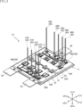
- the first control terminal 46E is a drain signal detection terminal (drain sense terminal) of the plurality of first semiconductor elements 10A.
- the voltage (voltage corresponding to the drain current) applied to each back electrode 15 (drain electrode) of the plurality of first semiconductor elements 10A is detected from the first control terminal 46E.
- the semiconductor device B1 converts the DC power supply voltage applied to the first power terminal 14 and the two second power terminals 15 into AC power using the plurality of semiconductor elements 21.
- the converted AC power is input from the two third power terminals 16 to a power supply target such as a motor.
- the two second power terminals 15 are separated from the first conductive part 1121 and the second conductive part 1122, respectively.
- the two second power terminals 15 each extend in the first direction x, and protrude from the sealing resin 50 in the x1 side of the first direction x.
- each of the two second power terminals 15 includes a portion covered with the sealing resin 50 and a portion exposed from the sealing resin 50.
- a second conductive member 32 is joined to a portion of each second power terminal 15 covered with the sealing resin 50 . Further, in each second power terminal 15, the portion exposed from the sealing resin 50 is used as the above-mentioned N terminal of the semiconductor device B1.
- each of the two third power terminals 16 includes a portion covered with the sealing resin 50 and a portion exposed from the sealing resin 50.
- a portion covered with the sealing resin 50 is joined to the second conductive portion 1122. Further, in each third power terminal 16, the portion exposed from the sealing resin 50 is used as the above-mentioned output terminal of the semiconductor device B1.
- the first control terminal 46B is a terminal (source sense terminal) for detecting source signals of the plurality of first elements 21A.
- the voltage (voltage corresponding to the source current) applied to each second electrode 212 (source electrode) of the plurality of first elements 21A is detected from the first control terminal 46B.
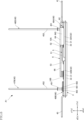
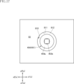
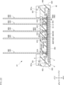
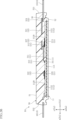
- the first flange portion 454 is connected to the end portion of the cylindrical portion 453 on the z1 side in the thickness direction z.
- the first flange portion 454 has a first surface 454a.
- the first surface 454a is a surface facing the z1 side in the thickness direction z.
- the first surface 454a is located at the end of the holder 451 on the z1 side in the thickness direction z.
- the first surface 454a has an annular shape (an annular shape in the illustrated example) when viewed in the thickness direction z.
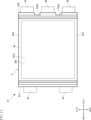
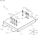
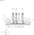
- FIG. 45 shows one step in the manufacturing process of the semiconductor device B1, and is a cross-sectional view similar to FIG. 44.
- a mold 91 for molding is provided with a cylindrical pin 911.
- the holder 451 is placed in the inner space of the cylindrical pin 911, and the mold is pressed while pressing the lower end of the cylindrical pin 911 (the end on the z2 side in the thickness direction z) against the control terminal support 48 (first metal layer 482).
- a fluid resin material is injected into the cavity space 919 of 91 .
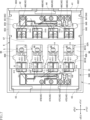
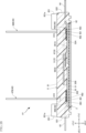
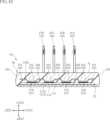
- each first recess 511 is filled with a first resin portion 55.
- the first resin portion 55 covers the holder 451 disposed in each first recess 511.
- the elastic modulus of the first resin portion 55 is smaller than the elastic modulus of the sealing resin 50. According to such a configuration, stress around the holder 451 covered by the first resin portion 55 can be reduced. Further, in the semiconductor device B12, by providing the first resin portion 55, it is possible to prevent foreign matter (including moisture) from entering the first recessed portion 511 exposed from the sealing resin 50.
- the semiconductor device B12 having the above configuration is preferable in terms of improving durability and reliability.
- the semiconductor device B12 has the same functions and effects as the semiconductor device B1 of the above embodiment within the same configuration range as the semiconductor device B1 of the above embodiment.
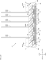
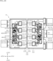
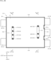
- FIG. 50 shows a semiconductor device according to a third modification of the first embodiment on the second side.
- FIG. 50 is a cross-sectional view showing the semiconductor device B13 of this modification, and is a cross-sectional view similar to FIG. 47.
- the semiconductor device B13 of this modification further includes a first resin portion 55, and differs from the semiconductor device B11 of the modification in that it includes the first resin portion 55.
- the first resin portion 55 fills at least a portion of the first recess 511 and contacts at least a portion of the holder 451. In the semiconductor device B13, the first resin portion 55 partially fills the first recess 511.
- the first resin part 55 covers a part of each of the plurality of holders 451 arranged in the first recess 511.
- the constituent material of the first resin portion 55 is not particularly limited.
- the first resin portion 55 may be made of the same material as the sealing resin 50, or may be made of a different material from the sealing resin 50. In the semiconductor device B13, for example, the constituent material of the first resin portion 55 is different from the constituent material of the sealing resin 50.
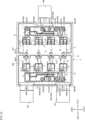
- the first resin portion 55 fills at least a portion of the first recess 511 and contacts at least a portion of the holder 451. In the semiconductor device B ⁇ b>14 , the first resin portion 55 is filled in each first recess 511 so as to fill each first recess 511 .
- the constituent material of the first resin portion 55 is not particularly limited.
- the first resin portion 55 may be made of the same material as the sealing resin 50, or may be made of a different material from the sealing resin 50. In the semiconductor device B14, for example, the constituent material of the first resin portion 55 is different from the constituent material of the sealing resin 50. In the semiconductor device B14, for example, the elastic modulus of the first resin portion 55 is smaller than the elastic modulus of the sealing resin 50. In this way, when the elastic modulus of the first resin part 55 is smaller than that of the sealing resin 50, the constituent material of the first resin part 55 is not particularly limited, and examples thereof include silicone resin, silicone gel, etc. .
- each control terminal 45 is entirely exposed from the sealing resin 50. According to such a configuration, it is possible to prevent the sealing resin 50 from flowing into the inside of the holder 451 into which the metal pin 452 is inserted. Therefore, in the semiconductor device B14, conduction between the holder 451 and the metal pins 452 can be maintained appropriately, and the control terminal 45 including the holder 451 and the metal pins 452 can function appropriately.
Abstract
Un dispositif à semi-conducteur selon la présente invention comprend au moins une borne. La borne comprend un support cylindrique ayant une conductivité, et une broche métallique insérée dans le support. Le dispositif à semi-conducteur comprend en outre un soutien de borne qui soutient le support, et une résine d'étanchéité qui recouvre le soutien de borne et une partie du support. La résine d'étanchéité comprend une surface principale de résine faisant face à un côté dans la direction de l'épaisseur. Le support comprend une première surface positionnée au niveau d'un bord de celui-ci sur un côté dans la direction de l'épaisseur, et une première surface latérale externe s'étendant dans la direction de l'épaisseur. La première surface est à une position différente de la surface principale de résine dans la direction de l'épaisseur. La première surface latérale externe est en contact avec la résine d'étanchéité. La broche métallique fait saillie davantage vers un côté dans la direction de l'épaisseur que la surface principale de résine.
Applications Claiming Priority (4)
| Application Number | Priority Date | Filing Date | Title |
|---|---|---|---|
| JP2022-075921 | 2022-05-02 | ||
| JP2022075921 | 2022-05-02 | ||
| JP2022-127149 | 2022-08-09 | ||
| JP2022127149 | 2022-08-09 |
Publications (1)
| Publication Number | Publication Date |
|---|---|
| WO2023214500A1 true WO2023214500A1 (fr) | 2023-11-09 |
Family
ID=88646429
Family Applications (1)
| Application Number | Title | Priority Date | Filing Date |
|---|---|---|---|
| PCT/JP2023/015070 WO2023214500A1 (fr) | 2022-05-02 | 2023-04-13 | Dispositif à semi-conducteur |
Country Status (1)
| Country | Link |
|---|---|
| WO (1) | WO2023214500A1 (fr) |
Citations (5)
| Publication number | Priority date | Publication date | Assignee | Title |
|---|---|---|---|---|
| JP2007184315A (ja) * | 2006-01-04 | 2007-07-19 | Hitachi Ltd | 樹脂封止型パワー半導体モジュール |
| JP2011165836A (ja) * | 2010-02-09 | 2011-08-25 | Mitsubishi Electric Corp | 電力用半導体装置 |
| JP2014123618A (ja) * | 2012-12-20 | 2014-07-03 | Mitsubishi Electric Corp | 半導体モジュール、その製造方法およびその接続方法 |
| US20190115275A1 (en) * | 2017-10-13 | 2019-04-18 | Semiconductor Components Industries, Llc | Semiconductor package and related methods |
| WO2022080063A1 (fr) * | 2020-10-14 | 2022-04-21 | ローム株式会社 | Module semi-conducteur |
-
2023
- 2023-04-13 WO PCT/JP2023/015070 patent/WO2023214500A1/fr unknown
Patent Citations (5)
| Publication number | Priority date | Publication date | Assignee | Title |
|---|---|---|---|---|
| JP2007184315A (ja) * | 2006-01-04 | 2007-07-19 | Hitachi Ltd | 樹脂封止型パワー半導体モジュール |
| JP2011165836A (ja) * | 2010-02-09 | 2011-08-25 | Mitsubishi Electric Corp | 電力用半導体装置 |
| JP2014123618A (ja) * | 2012-12-20 | 2014-07-03 | Mitsubishi Electric Corp | 半導体モジュール、その製造方法およびその接続方法 |
| US20190115275A1 (en) * | 2017-10-13 | 2019-04-18 | Semiconductor Components Industries, Llc | Semiconductor package and related methods |
| WO2022080063A1 (fr) * | 2020-10-14 | 2022-04-21 | ローム株式会社 | Module semi-conducteur |
Similar Documents
| Publication | Publication Date | Title |
|---|---|---|
| US9129931B2 (en) | Power semiconductor module and power unit device | |
| US8546926B2 (en) | Power converter | |
| US10861833B2 (en) | Semiconductor device | |
| WO2018194090A1 (fr) | Dispositif à semi-conducteur | |
| US20130249008A1 (en) | Semiconductor device | |
| JP2020519027A (ja) | 半導体モジュール | |
| US20130256920A1 (en) | Semiconductor device | |
| WO2023214500A1 (fr) | Dispositif à semi-conducteur | |
| JP4695041B2 (ja) | 半導体装置 | |
| JP7190985B2 (ja) | 半導体装置 | |
| JP7392319B2 (ja) | 半導体装置 | |
| WO2021010210A1 (fr) | Dispositif à semi-conducteur | |
| WO2024024372A1 (fr) | Dispositif à semi-conducteur, unité de conversion de puissance électrique et procédé de fabrication de dispositif à semi-conducteur | |
| WO2023017707A1 (fr) | Dispositif à semi-conducteurs | |
| WO2023140050A1 (fr) | Dispositif à semi-conducteur | |
| WO2023017708A1 (fr) | Dispositif à semi-conducteurs | |
| WO2022264834A1 (fr) | Dispositif à semi-conducteurs | |
| JP4861200B2 (ja) | パワーモジュール | |
| US20240136320A1 (en) | Semiconductor device | |
| WO2024075589A1 (fr) | Dispositif à semi-conducteur | |
| WO2023190180A1 (fr) | Dispositif à semi-conducteur | |
| WO2024024378A1 (fr) | Dispositif à semi-conducteur | |
| WO2023243464A1 (fr) | Dispositif à semi-conducteur, module à semi-conducteur et structure de montage de module à semi-conducteur | |
| WO2024075514A1 (fr) | Structure de jonction et dispositif à semi-conducteur | |
| WO2023189840A1 (fr) | Dispositif à semi-conducteur |
Legal Events
| Date | Code | Title | Description |
|---|---|---|---|
| 121 | Ep: the epo has been informed by wipo that ep was designated in this application |
Ref document number: 23799432 Country of ref document: EP Kind code of ref document: A1 |