WO2024075514A1 - Structure de jonction et dispositif à semi-conducteur - Google Patents
Structure de jonction et dispositif à semi-conducteur Download PDFInfo
- Publication number
- WO2024075514A1 WO2024075514A1 PCT/JP2023/033925 JP2023033925W WO2024075514A1 WO 2024075514 A1 WO2024075514 A1 WO 2024075514A1 JP 2023033925 W JP2023033925 W JP 2023033925W WO 2024075514 A1 WO2024075514 A1 WO 2024075514A1
- Authority
- WO
- WIPO (PCT)
- Prior art keywords
- layer
- bonding
- bonded
- surface layer
- wiring
- Prior art date
Links
- 238000005304 joining Methods 0.000 title claims abstract description 21
- 239000004065 semiconductor Substances 0.000 title claims description 107
- 239000010410 layer Substances 0.000 claims abstract description 347
- 239000002344 surface layer Substances 0.000 claims abstract description 149
- 239000000463 material Substances 0.000 claims abstract description 104
- 239000000758 substrate Substances 0.000 claims description 70
- 239000007790 solid phase Substances 0.000 abstract 2
- 229920005989 resin Polymers 0.000 description 82
- 239000011347 resin Substances 0.000 description 82
- 229910052751 metal Inorganic materials 0.000 description 74
- 239000002184 metal Substances 0.000 description 74
- 239000004020 conductor Substances 0.000 description 38
- 239000010949 copper Substances 0.000 description 37
- 239000012790 adhesive layer Substances 0.000 description 34
- 239000000853 adhesive Substances 0.000 description 32
- 230000001070 adhesive effect Effects 0.000 description 32
- 238000001514 detection method Methods 0.000 description 30
- 229910052709 silver Inorganic materials 0.000 description 22
- 239000004332 silver Substances 0.000 description 22
- 229910052802 copper Inorganic materials 0.000 description 14
- RYGMFSIKBFXOCR-UHFFFAOYSA-N Copper Chemical compound [Cu] RYGMFSIKBFXOCR-UHFFFAOYSA-N 0.000 description 13
- 239000011800 void material Substances 0.000 description 7
- 229910000881 Cu alloy Inorganic materials 0.000 description 5
- 229910052782 aluminium Inorganic materials 0.000 description 5
- 239000000919 ceramic Substances 0.000 description 5
- XAGFODPZIPBFFR-UHFFFAOYSA-N aluminium Chemical compound [Al] XAGFODPZIPBFFR-UHFFFAOYSA-N 0.000 description 4
- 239000000470 constituent Substances 0.000 description 4
- 238000000465 moulding Methods 0.000 description 4
- PXHVJJICTQNCMI-UHFFFAOYSA-N nickel Substances [Ni] PXHVJJICTQNCMI-UHFFFAOYSA-N 0.000 description 4
- 238000003825 pressing Methods 0.000 description 4
- 229910052581 Si3N4 Inorganic materials 0.000 description 3
- PNEYBMLMFCGWSK-UHFFFAOYSA-N aluminium oxide Inorganic materials [O-2].[O-2].[O-2].[Al+3].[Al+3] PNEYBMLMFCGWSK-UHFFFAOYSA-N 0.000 description 3
- PMHQVHHXPFUNSP-UHFFFAOYSA-M copper(1+);methylsulfanylmethane;bromide Chemical compound Br[Cu].CSC PMHQVHHXPFUNSP-UHFFFAOYSA-M 0.000 description 3
- HBMJWWWQQXIZIP-UHFFFAOYSA-N silicon carbide Chemical compound [Si+]#[C-] HBMJWWWQQXIZIP-UHFFFAOYSA-N 0.000 description 3
- 229910010271 silicon carbide Inorganic materials 0.000 description 3
- HQVNEWCFYHHQES-UHFFFAOYSA-N silicon nitride Chemical compound N12[Si]34N5[Si]62N3[Si]51N64 HQVNEWCFYHHQES-UHFFFAOYSA-N 0.000 description 3
- 229910000679 solder Inorganic materials 0.000 description 3
- 229910002601 GaN Inorganic materials 0.000 description 2
- JMASRVWKEDWRBT-UHFFFAOYSA-N Gallium nitride Chemical compound [Ga]#N JMASRVWKEDWRBT-UHFFFAOYSA-N 0.000 description 2
- MCMNRKCIXSYSNV-UHFFFAOYSA-N Zirconium dioxide Chemical compound O=[Zr]=O MCMNRKCIXSYSNV-UHFFFAOYSA-N 0.000 description 2
- 239000002390 adhesive tape Substances 0.000 description 2
- 229910052593 corundum Inorganic materials 0.000 description 2
- 239000003822 epoxy resin Substances 0.000 description 2
- 230000005669 field effect Effects 0.000 description 2
- 239000012530 fluid Substances 0.000 description 2
- 239000010931 gold Substances 0.000 description 2
- 229910044991 metal oxide Inorganic materials 0.000 description 2
- 150000004706 metal oxides Chemical class 0.000 description 2
- 238000000034 method Methods 0.000 description 2
- 229920000647 polyepoxide Polymers 0.000 description 2
- 229910001845 yogo sapphire Inorganic materials 0.000 description 2
- 239000004593 Epoxy Substances 0.000 description 1
- 239000004642 Polyimide Substances 0.000 description 1
- NIXOWILDQLNWCW-UHFFFAOYSA-N acrylic acid group Chemical group C(C=C)(=O)O NIXOWILDQLNWCW-UHFFFAOYSA-N 0.000 description 1
- 239000000654 additive Substances 0.000 description 1
- 230000000996 additive effect Effects 0.000 description 1
- 229910045601 alloy Inorganic materials 0.000 description 1
- 239000000956 alloy Substances 0.000 description 1
- 230000007423 decrease Effects 0.000 description 1
- 229910003460 diamond Inorganic materials 0.000 description 1
- 239000010432 diamond Substances 0.000 description 1
- 238000009792 diffusion process Methods 0.000 description 1
- 239000011521 glass Substances 0.000 description 1
- PCHJSUWPFVWCPO-UHFFFAOYSA-N gold Chemical compound [Au] PCHJSUWPFVWCPO-UHFFFAOYSA-N 0.000 description 1
- 229910052737 gold Inorganic materials 0.000 description 1
- 230000005484 gravity Effects 0.000 description 1
- 230000017525 heat dissipation Effects 0.000 description 1
- 238000003780 insertion Methods 0.000 description 1
- 230000037431 insertion Effects 0.000 description 1
- 230000002452 interceptive effect Effects 0.000 description 1
- 238000004519 manufacturing process Methods 0.000 description 1
- 150000002739 metals Chemical class 0.000 description 1
- 229910052759 nickel Inorganic materials 0.000 description 1
- TWNQGVIAIRXVLR-UHFFFAOYSA-N oxo(oxoalumanyloxy)alumane Chemical compound O=[Al]O[Al]=O TWNQGVIAIRXVLR-UHFFFAOYSA-N 0.000 description 1
- 238000007747 plating Methods 0.000 description 1
- 229920001721 polyimide Polymers 0.000 description 1
- 229920001296 polysiloxane Polymers 0.000 description 1
- 239000003566 sealing material Substances 0.000 description 1
- 229910052710 silicon Inorganic materials 0.000 description 1
- 239000010703 silicon Substances 0.000 description 1
- 125000006850 spacer group Chemical group 0.000 description 1
Images


Classifications
-
- B—PERFORMING OPERATIONS; TRANSPORTING
- B23—MACHINE TOOLS; METAL-WORKING NOT OTHERWISE PROVIDED FOR
- B23K—SOLDERING OR UNSOLDERING; WELDING; CLADDING OR PLATING BY SOLDERING OR WELDING; CUTTING BY APPLYING HEAT LOCALLY, e.g. FLAME CUTTING; WORKING BY LASER BEAM
- B23K20/00—Non-electric welding by applying impact or other pressure, with or without the application of heat, e.g. cladding or plating
-
- H—ELECTRICITY
- H01—ELECTRIC ELEMENTS
- H01L—SEMICONDUCTOR DEVICES NOT COVERED BY CLASS H10
- H01L21/00—Processes or apparatus adapted for the manufacture or treatment of semiconductor or solid state devices or of parts thereof
- H01L21/02—Manufacture or treatment of semiconductor devices or of parts thereof
- H01L21/04—Manufacture or treatment of semiconductor devices or of parts thereof the devices having potential barriers, e.g. a PN junction, depletion layer or carrier concentration layer
- H01L21/50—Assembly of semiconductor devices using processes or apparatus not provided for in a single one of the subgroups H01L21/06 - H01L21/326, e.g. sealing of a cap to a base of a container
- H01L21/52—Mounting semiconductor bodies in containers
-
- H—ELECTRICITY
- H01—ELECTRIC ELEMENTS
- H01L—SEMICONDUCTOR DEVICES NOT COVERED BY CLASS H10
- H01L23/00—Details of semiconductor or other solid state devices
- H01L23/34—Arrangements for cooling, heating, ventilating or temperature compensation ; Temperature sensing arrangements
- H01L23/40—Mountings or securing means for detachable cooling or heating arrangements ; fixed by friction, plugs or springs
Definitions
- This disclosure relates to a joint structure and a semiconductor device.
- Patent Document 1 discloses a conventional semiconductor device (power module).
- the power module described in Patent Document 1 includes multiple transistors, a main board, a signal board, and signal terminals. The multiple transistors are mounted on the main board.
- a joining structure is used to join two objects to be joined. It is preferable for the joining structure to achieve a reliable joining while also being able to easily transfer heat.
- An object of the present disclosure is to provide a joint structure that is improved over conventional structures, and thus a semiconductor device that includes such a joint structure.
- an object of the present disclosure is to provide a joint structure (and thus a semiconductor device) that is more easily able to transmit heat.
- the bonded structure provided by the first aspect of the present disclosure includes a first object to be bonded having a first bonding layer, a second object to be bonded having a second bonding layer, and an intermediate bonding material interposed between the first object to be bonded and the second object to be bonded.
- the intermediate bonding material has a base layer and a first surface layer and a second surface layer disposed on either side of the base layer.
- the first bonding layer and the first surface layer are bonded by solid-state bonding.
- the second bonding layer and the second surface layer are bonded by solid-state bonding.
- the base layer is mainly composed of Cu.
- the above configuration makes it possible to provide a joint structure that is more easily able to transfer heat, and in turn a semiconductor device that includes such a joint structure.
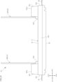
- FIG. 1 is a perspective view showing a semiconductor device according to a first embodiment of the present disclosure.
- FIG. 2 is a partial perspective view showing the semiconductor device according to the first embodiment of the present disclosure.
- FIG. 3 is a partial perspective view showing the semiconductor device according to the first embodiment of the present disclosure.
- FIG. 4 is a plan view showing the semiconductor device according to the first embodiment of the present disclosure.
- FIG. 5 is a partial plan view showing the semiconductor device according to the first embodiment of the present disclosure.
- FIG. 6 is a partial right side view showing the semiconductor device according to the first embodiment of the present disclosure.
- FIG. 7 is a partial left side view showing the semiconductor device according to the first embodiment of the present disclosure.
- FIG. 8 is a partial plan view showing the semiconductor device according to the first embodiment of the present disclosure.
- FIG. 1 is a perspective view showing a semiconductor device according to a first embodiment of the present disclosure.
- FIG. 2 is a partial perspective view showing the semiconductor device according to the first embodiment of the present disclosure.
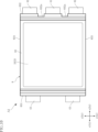
- FIG. 9 is a right side view showing the semiconductor device according to the first embodiment of the present disclosure.
- FIG. 10 is a bottom view showing the semiconductor device according to the first embodiment of the present disclosure.
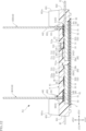
- FIG. 11 is a cross-sectional view taken along line XI-XI of FIG.
- FIG. 12 is a cross-sectional view taken along line XII-XII in FIG.
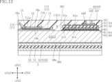
- FIG. 13 is a partially enlarged cross-sectional view of a part of FIG.
- FIG. 14 is a partially enlarged cross-sectional view showing an example of a mounting structure according to the first embodiment of the present disclosure.
- FIG. 15 is a partially enlarged cross-sectional view showing another example of the mounting structure according to the first embodiment of the present disclosure.
- FIG. 16 is a partially enlarged cross-sectional view of a portion of FIG.
- FIG. 17 is a partially enlarged cross-sectional view showing another example of the mounting structure according to the first embodiment of the present disclosure.
- FIG. 18 is a partially enlarged cross-sectional view showing another example of the mounting structure according to the first embodiment of the present disclosure.
- FIG. 19 is a cross-sectional view taken along line XIX-XIX in FIG.
- FIG. 20 is a cross-sectional view taken along line XX-XX in FIG.
- FIG. 21 is a cross-sectional view taken along line XXI-XXI in FIG.
- FIG. 22 is a cross-sectional view taken along line XXII-XXII in FIG.
- FIG. 23 is a partial right side view showing a first modified example of the semiconductor device according to the first embodiment of the present disclosure.
- FIG. 24 is a partially enlarged cross-sectional view showing another example of the mounting structure according to the first embodiment of the present disclosure.
- FIG. 25 is a partially enlarged cross-sectional view showing a mounting structure according to the second embodiment of the present disclosure.
- an object A is formed on an object B
- an object A is formed on (an object B)
- an object A is formed directly on an object B
- an object A is formed on an object B with another object interposed between the object A and the object B” unless otherwise specified.
- an object A is disposed on an object B” and “an object A is disposed on (an object B)” include “an object A is disposed directly on an object B” and “an object A is disposed on (an object B) with another object interposed between the object A and the object B” unless otherwise specified.
- an object A is located on (an object B) includes “an object A is in contact with an object B and is located on (an object B)” and “an object A is located on (an object B) with another object interposed between the object A and the object B”.
- object A overlaps object B includes “object A overlaps the entirety of object B” and “object A overlaps part of object B.”
- the semiconductor device A1 includes a plurality of semiconductor elements 1, a supporting conductor 2, a supporting substrate 3, a plurality of power terminals 41 to 43, a plurality of control terminals 44, a signal substrate 5, an adhesive layer 6, a first conductive member 71, a second conductive member 72, a plurality of wires 73 to 76, a resin member 8, and a resin filling portion 88.
- the semiconductor device A1 also has joint structures B1 to B4.
- the support conductor 2 includes a first conductive portion 2A and a second conductive portion 2B.
- the multiple control terminals 44 include a multiple first control terminals 45 and a multiple second control terminals 46.
- the signal board 5 includes a first signal board 5A and a second signal board 5B.
- the adhesive layer 6 includes a first adhesive body 6A and a second adhesive body 6B.
- the three mutually orthogonal directions are referred to as the x-direction, y-direction, and z-direction.
- the z-direction is the thickness direction of the semiconductor device A1.
- the x-direction is the left-right direction in the plan view of the semiconductor device A1 (see FIG. 4).
- the y-direction is the up-down direction in the plan view of the semiconductor device A1 (see FIG. 4).
- “plan view” refers to the view in the z-direction. Note that the terms "upper”, “lower”, “upper”, “lower”, “top surface”, and “bottom surface” indicate the relative positional relationship of each component, etc. in the z-direction, and do not necessarily define the relationship with the direction of gravity.
- the x-direction is an example of a "first direction” in this disclosure.
- Each of the semiconductor elements 1 is an electronic component that is the core of the function of the semiconductor device A1.
- the material of each of the semiconductor elements 1 is, for example, a semiconductor material mainly made of SiC (silicon carbide). This semiconductor material is not limited to SiC, and may be Si (silicon), GaN (gallium nitride), or C (diamond).
- Each of the semiconductor elements 1 is, for example, a power semiconductor chip having a switching function such as a MOSFET (Metal Oxide Semiconductor Field Effect Transistor).
- MOSFET Metal Oxide Semiconductor Field Effect Transistor
- each of the semiconductor elements 1 is a MOSFET
- other transistors such as an IGBT (Insulated Gate Bipolar Transistor) may also be used.
- Each of the semiconductor elements 1 is the same element.
- Each of the semiconductor elements 1 is, for example, an n-channel MOSFET, but may also be a p-channel MOSFET.
- the multiple semiconductor elements 1 include multiple first switching elements 1A and multiple second switching elements 1B. As shown in FIG. 8, the semiconductor device A1 has four first switching elements 1A and four second switching elements 1B, but the number of first switching elements 1A and the number of second switching elements 1B are not limited to this configuration. The number of first switching elements 1A and the number of second switching elements 1B are changed as appropriate depending on the performance required of the semiconductor device A1. The number of first switching elements 1A and the number of second switching elements 1B may be equal or different. The number of first switching elements 1A and the number of second switching elements 1B are determined by the current capacity handled by the semiconductor device A1.
- the semiconductor device A1 is configured, for example, as a half-bridge type switching circuit.
- the multiple first switching elements 1A configure the upper arm circuit of the semiconductor device A1
- the multiple second switching elements 1B configure the lower arm circuit of the semiconductor device A1.
- the multiple first switching elements 1A are connected in parallel with each other, and in the lower arm circuit, the multiple second switching elements 1B are connected in parallel with each other.
- each first switching element 1A and each second switching element 1B are connected in series.
- each of the multiple semiconductor elements 1 has an element main surface 10a and an element back surface 10b.
- the element main surface 10a and the element back surface 10b are spaced apart in the z direction.
- the element main surface 10a faces the z2 side
- the element back surface 10b faces the z1 side.
- the multiple first switching elements 1A are each mounted on a support conductor 2 (first conductive portion 2A) as shown in Figures 8, 12, 13, 21, etc. In the example shown in Figure 8, the multiple first switching elements 1A are arranged, for example, in the y direction and spaced apart from one another. Each of the multiple first switching elements 1A is conductively joined to the support conductor 2 (first conductive portion 2A) via an intermediate bonding material 19a. When each first switching element 1A is joined to the first conductive portion 2A, the element back surface 10b faces the support conductor 2 (first conductive portion 2A).
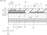
- the second switching elements 1B are mounted on the support conductor 2 (second conductive portion 2B) as shown in FIG. 8, FIG. 12, FIG. 16, FIG. 20, etc.
- the second switching elements 1B are arranged, for example, in the y direction and spaced apart from each other.
- the second switching elements 1B are each conductively joined to the support conductor 2 (second conductive portion 2B) via an intermediate joining material 19b.
- the element back surface 10b faces the support conductor 2 (second conductive portion 2B).
- the first switching elements 1A and the second switching elements 1B overlap when viewed in the x direction. Unlike this configuration, the first switching elements 1A and the second switching elements 1B do not have to overlap when viewed in the x direction.
- the semiconductor elements 1 each have a first principal surface electrode 11, a second principal surface electrode 12, a third principal surface electrode 13, and a back surface electrode 15, as shown in FIG. 8, FIG. 13, and FIG. 16.
- the configurations of the first principal surface electrode 11, the second principal surface electrode 12, the third principal surface electrode 13, and the back surface electrode 15 described below are common to all the semiconductor elements 1.
- the first principal surface electrode 11, the second principal surface electrode 12, and the third principal surface electrode 13 are provided on the element principal surface 10a.
- the first principal surface electrode 11, the second principal surface electrode 12, and the third principal surface electrode 13 are insulated by an insulating film (not shown).
- the back surface electrode 15 is provided on the element back surface 10b.
- the back surface electrode 15 covers the entire area (or substantially the entire area) of the element back surface 10b.
- the back surface electrode 15 is formed, for example, by Ag (silver) plating.
- the first principal surface electrode 11 is, for example, a gate electrode to which a drive signal (for example, a gate voltage) for driving each semiconductor element 1 is input.
- the second principal surface electrode 12 is, for example, a source electrode through which a source current flows.
- the third principal surface electrode 13 is, for example, a source sense electrode, and has the same potential as the second principal surface electrode 12.
- the third principal surface electrode 13 has the same source current as the second principal surface electrode 12.
- the back surface electrode 15 is, for example, a drain electrode through which a drain current flows.
- each semiconductor element 1 switches between a conductive state and a cut-off state in response to the drive signal.
- This operation of switching between a conductive state and a cut-off state is called a switching operation.
- a forward current flows from the back surface electrode 15 (drain electrode) to the second principal surface electrode 12 (source electrode), and in the cut-off state, this forward current does not flow.
- the semiconductor device A1 converts a first power supply voltage (e.g., a DC voltage) into a second power supply voltage (e.g., an AC voltage) by the function of each semiconductor element 1.
- the first power supply voltage is input (applied) between the power terminal 41 and the two power terminals 42, and the second power supply voltage is input (applied) to the two power terminals 43.
- the semiconductor device A1 has two thermistors 17. Each thermistor 17 is used as a sensor for detecting temperature.
- Support conductor 2 supports the multiple semiconductor elements 1 (the multiple first switching elements 1A and the multiple second switching elements 1B).
- the supporting conductor 2 is joined onto a supporting substrate 3.
- the supporting conductor 2 has, for example, a rectangular shape in a plan view.
- the support conductor 2 includes a first conductive portion 2A and a second conductive portion 2B.
- the first conductive portion 2A has a main body layer 20A, a bonding layer 21A, and a bonding layer 22A.
- the second conductive portion 2B has a main body layer 20B, a bonding layer 21B, and a bonding layer 22B.
- the main body layer 20A and the main body layer 20B are each a plate-shaped member made of metal. This metal is Cu (copper) or a Cu alloy.
- the first conductive portion 2A and the second conductive portion 2B together with the multiple power terminals 41 to 43, form a conduction path to the multiple first switching elements 1A and the multiple second switching elements 1B.
- the first conductive portion 2A and the second conductive portion 2B are each, for example, rectangular in a plan view.
- the first conductive portion 2A and the second conductive portion 2B each have, for example, a dimension in the x direction of 15 mm or more and 25 mm or less, a dimension in the y direction of 30 mm or more and 40 mm or less, and a dimension in the z direction of 1.0 mm or more and 5.0 mm or less (preferably about 2.0 mm).
- These dimensions of the first conductive portion 2A and the second conductive portion 2B are not limited to the numerical examples given above, and can be changed as appropriate according to the specifications of the semiconductor device A1.
- the first conductive portion 2A is bonded to the support substrate 3 via an intermediate bonding material 29a
- the second conductive portion 2B is bonded to the support substrate 3 via an intermediate bonding material 29b.
- a plurality of first switching elements 1A are bonded to the first conductive portion 2A via an intermediate bonding material 19a.
- a plurality of second switching elements 1B are bonded to the second conductive portion 2B via an intermediate bonding material 19b.
- the first conductive portion 2A and the second conductive portion 2B are spaced apart in the x direction as shown in Figs. 3, 8, 11, 12, and 19. In the examples shown in these figures, the first conductive portion 2A is located on the x1 side of the second conductive portion 2B.
- the first conductive portion 2A and the second conductive portion 2B overlap when viewed in the x direction.
- the support conductor 2 (each of the first conductive portion 2A and the second conductive portion 2B) has a main surface 201 and a back surface 202. As shown in Figures 11 to 22, the main surface 201 and the back surface 202 are spaced apart in the z direction. The main surface 201 faces the z2 side, and the back surface 202 faces the z1 side. The back surface 202 faces the support substrate 3.
- the semiconductor device A1 has a joint structure B11.
- the joint structure B11 is a structure in which a first switching element 1A as a first joint object and a first conductive portion 2A as a second joint object are joined via an intermediate joint material 19a.
- the intermediate bonding material 19a has a base layer 190a, a first surface layer 191a, and a second surface layer 192a.
- the base material layer 190a is mainly composed of Cu (copper).
- Configurations in which the base material layer 190a is mainly composed of Cu (copper) include configurations made of only Cu (copper), configurations in which an additive metal is added to Cu (copper), and various Cu (copper) alloys. The same applies to configurations in which "a certain member is mainly composed of a certain metal" in the following explanation.
- the thickness of the base material layer 190a is, for example, 50 ⁇ m or more and 300 ⁇ m or less.
- the first surface layer 191a is disposed on the z2 side of the base layer 190a in the z direction.
- the first surface layer 191a is solid-state bonded to the first switching element 1A.
- Solid-state bonding is a bonding method that is achieved by applying a predetermined pressure and temperature to two layers that are mainly made of the same metal and are in direct contact with each other, and includes, for example, solid-state diffusion bonding and solid-state deformation bonding.
- the first surface layer 191a is mainly made of Ag (silver).
- the first surface layer 191a is thinner than the base layer 190a.
- the thickness of the first surface layer 191a is, for example, 0.1 ⁇ m or more and 15 ⁇ m or less.
- the first switching element 1A further has a bonding layer 151.
- the bonding layer 151 corresponds to the first bonding layer in the bonding structure B11.
- the bonding layer 151 is disposed on the z1 side of the back electrode 15 in the z direction.
- the bonding layer 151 is solid-state bonded to the first surface layer 191a.
- the bonding layer 151 is mainly composed of Ag (silver).
- the thickness of the bonding layer 151 is, for example, 0.01 ⁇ m or more and 5 ⁇ m or less.
- the metal that is the main component of the first surface layer 191a and the bonding layer 151 is not limited in any way, so long as they are configured to be solid-state bonded to each other.
- the boundary between the first surface layer 191a and the bonding layer 151, which are solid-state bonded to each other, is less clear than, for example, the boundary between the base material layer 190a and the first surface layer 191a, which is the boundary between dissimilar metals.
- the boundary between the first surface layer 191a and the bonding layer 151 is barely discernible, or is only discernible due to the presence of a small gap or the like that occurs during solid-state bonding.
- the second surface layer 192a is disposed on the z1 side of the base layer 190a in the z direction.
- the second surface layer 192a is solid-state bonded to the first conductive portion 2A.
- the second surface layer 192a is mainly composed of Ag (silver).
- the second surface layer 192a is thinner than the base layer 190a.
- the thickness of the second surface layer 192a is, for example, 0.1 ⁇ m or more and 15 ⁇ m or less.
- the bonding layer 21A of the first conductive portion 2A corresponds to the second bonding layer in the bonded structure B11.
- the bonding layer 21A is disposed on the z2 side of the main body layer 20A in the z direction.
- the bonding layer 21A is solid-state bonded to the second surface layer 192a.
- the bonding layer 21A is mainly composed of Ag (silver).
- the thickness of the bonding layer 21A is, for example, 0.1 ⁇ m or more and 15 ⁇ m or less.
- the metal that is the main component of the second surface layer 192a and the bonding layer 21A is not limited in any way, so long as they are configured to be solid-state bonded to each other.
- the semiconductor device A1 has a joint structure B12.
- the joint structure B12 is a structure in which a second switching element 1B as a first joint object and a second conductive part 2B as a second joint object are joined via an intermediate joint material 19b.
- the intermediate bonding material 19b has a base layer 190b, a first surface layer 191b, and a second surface layer 192b.
- the base material layer 190b is mainly composed of Cu (copper). There are no limitations on the thickness of the base material layer 190b, and in this embodiment, the base material layer 190b is thicker than the first surface layer 191b and the second surface layer 192b. The thickness of the base material layer 190b is, for example, 50 ⁇ m or more and 300 ⁇ m or less.
- the first surface layer 191b is disposed on the z2 side of the base layer 190b in the z direction.
- the first surface layer 191b is solid-state bonded to the second switching element 1B.
- the first surface layer 191b is mainly composed of Ag (silver).
- the first surface layer 191b is thinner than the base layer 190b.
- the thickness of the first surface layer 191b is, for example, 0.1 ⁇ m or more and 15 ⁇ m or less.
- the second switching element 1B further has a bonding layer 151 similar to that of the first switching element 1A.
- the bonding layer 151 of the second switching element 1B is solid-state bonded to the first surface layer 191b.
- the metal that is the main component of the first surface layer 191b and the bonding layer 151 is not limited in any way, so long as they are configured to be solid-state bonded to each other.
- the second surface layer 192b is disposed on the z1 side of the base layer 190b in the z direction.
- the second surface layer 192b is solid-state bonded to the second conductive portion 2B.
- the second surface layer 192b is mainly composed of Ag (silver).
- the second surface layer 192b is thinner than the base layer 190b.
- the thickness of the second surface layer 192b is, for example, 0.1 ⁇ m or more and 15 ⁇ m or less.
- the bonding layer 21B of the second conductive portion 2B corresponds to the second bonding layer in the bonding structure B12.
- the bonding layer 21B is disposed on the z2 side of the main body layer 20B in the z direction.
- the bonding layer 21B is solid-state bonded to the second surface layer 192b.
- the bonding layer 21B is mainly composed of Ag (silver).
- the thickness of the bonding layer 21B is, for example, 0.1 ⁇ m or more and 15 ⁇ m or less.
- the metal that is the main component of the second surface layer 192b and the bonding layer 21B there are no limitations on the metal that is the main component of the second surface layer 192b and the bonding layer 21B, as long as they are configured to be solid-state bonded to each other.
- the support substrate 3 supports the support conductor 2.
- the support substrate 3 is, for example, a direct bonded copper (DBC) substrate.
- the support substrate 3 may be, for example, a direct bonded aluminum (DBA) substrate.
- the support substrate 3 includes an insulating layer 31, a first metal layer 32, and a second metal layer 33.
- the insulating layer 31 is made of, for example, a ceramic with excellent thermal conductivity. Examples of such ceramics include AlN (aluminum nitride), SiN (silicon nitride), Al2O3 (aluminum oxide), and ZTA (zirconia reinforced alumina).
- the insulating layer 31 may be made of an insulating resin instead of ceramic.
- the insulating layer 31 is, for example, rectangular in plan view.
- the first metal layer 32 is formed on the upper surface (surface facing the z2 side) of the insulating layer 31.
- the constituent material of the first metal layer 32 includes, for example, Cu.
- the constituent material may include Al (aluminum) instead of Cu.
- the first metal layer 32 includes a first portion 32A and a second portion 32B.
- the first portion 32A and the second portion 32B are spaced apart in the x direction.
- the first portion 32A is located on the x1 side of the second portion 32B.
- the first conductive portion 2A is joined to the first portion 32A and supports the first conductive portion 2A.
- the second portion 32B is joined to the second conductive portion 2B and supports the second conductive portion 2B.
- the first portion 32A and the second portion 32B are each, for example, rectangular in a plan view.
- the second metal layer 33 is formed on the lower surface (surface facing the z1 side) of the insulating layer 31.
- the constituent material of the second metal layer 33 is the same as the constituent material of the first metal layer 32.
- the lower surface (surface facing the z1 side) of the second metal layer 33 is exposed from the resin member 8 as shown in Figures 10 to 22.
- a heat dissipation member e.g., a heat sink
- the second metal layer 33 overlaps both the first portion 32A and the second portion 32B in a plan view.
- the joint structure B13 is a structure in which a first conductive part 2A as a first object to be joined and a supporting substrate 3 as a second object to be joined are joined via an intermediate joining material 29a.
- the intermediate bonding material 29a has a base layer 290a, a first surface layer 291a, and a second surface layer 292a.
- the base material layer 290a is mainly composed of Cu (copper). There are no limitations on the thickness of the base material layer 290a, and in this embodiment, the base material layer 290a is thicker than the first surface layer 291a and the second surface layer 292a. The thickness of the base material layer 290a is, for example, 50 ⁇ m or more and 300 ⁇ m or less.
- the first surface layer 291a is disposed on the z2 side of the base layer 290a in the z direction.
- the first surface layer 291a is solid-state bonded to the first conductive portion 2A.
- the first surface layer 291a is mainly composed of Ag (silver).
- Ag silver
- the thickness of the first surface layer 291a is, for example, 0.1 ⁇ m or more and 15 ⁇ m or less.
- the bonding layer 22A of the first conductive portion 2A corresponds to the first bonding layer in the bonding structure B13.
- the bonding layer 22A is disposed on the z1 side of the main body layer 20A in the z direction.
- the bonding layer 22A is solid-state bonded to the first surface layer 291a.
- the bonding layer 22A is mainly composed of Ag (silver).
- the thickness of the bonding layer 22A is, for example, 0.1 ⁇ m or more and 15 ⁇ m or less.
- the metal that is the main component of the first surface layer 291a and the bonding layer 22A is not limited in any way, so long as they are configured to be solid-state bonded to each other.
- the second surface layer 292a is disposed on the z1 side of the base layer 290a in the z direction.
- the second surface layer 292a is solid-state bonded to the support substrate 3.
- the second surface layer 292a is mainly composed of Ag (silver).
- the second surface layer 292a is thinner than the base layer 290a.
- the thickness of the second surface layer 292a is, for example, 0.1 ⁇ m or more and 15 ⁇ m or less.
- the support substrate 3 of this embodiment further includes a bonding layer 321A.
- the bonding layer 321A corresponds to the second bonding layer in the bonded structure B13.
- the bonding layer 321A is disposed on the z2 side of the first portion 32A in the z direction.
- the bonding layer 321A is solid-state bonded to the second surface layer 292a.
- the bonding layer 321A is mainly composed of Ag (silver).
- the thickness of the bonding layer 321A is, for example, 0.1 ⁇ m or more and 15 ⁇ m or less.
- the semiconductor device A1 has a joint structure B14.
- the joint structure B14 is a structure in which the second conductive part 2B as the first joint object and the support substrate 3 as the second joint object are joined via an intermediate joint material 29b.
- the intermediate bonding material 29b has a base layer 290b, a first surface layer 291b, and a second surface layer 292b.
- the base material layer 290b is mainly composed of Cu (copper). There are no limitations on the thickness of the base material layer 290b, and in this embodiment, the base material layer 290b is thicker than the first surface layer 291b and the second surface layer 292b. The thickness of the base material layer 290b is, for example, 50 ⁇ m or more and 300 ⁇ m or less.
- the first surface layer 291b is disposed on the z2 side of the base layer 290b in the z direction.
- the first surface layer 291b is solid-state bonded to the second switching element 1B.
- the first surface layer 291b is mainly composed of Ag (silver).
- the first surface layer 291b is thinner than the base layer 290b.
- the thickness of the first surface layer 291b is, for example, 0.1 ⁇ m or more and 15 ⁇ m or less.
- the bonding layer 22B of the second conductive portion 2B corresponds to the first bonding layer in the bonding structure B14.
- the bonding layer 22B is disposed on the z1 side of the main body layer 20B in the z direction.
- the bonding layer 22B is solid-state bonded to the first surface layer 291b.
- the bonding layer 22B is mainly composed of Ag (silver).
- the thickness of the bonding layer 22B is, for example, 0.1 ⁇ m or more and 15 ⁇ m or less.
- the second surface layer 292b is disposed on the z1 side of the base layer 290b in the z direction.
- the second surface layer 292b is solid-state bonded to the support substrate 3.
- the second surface layer 292b is mainly composed of Ag (silver).
- the second surface layer 292b is thinner than the base layer 290b.
- the thickness of the second surface layer 292b is, for example, 0.1 ⁇ m or more and 15 ⁇ m or less.
- the support substrate 3 of this embodiment further includes a bonding layer 321B.
- the bonding layer 321B corresponds to the second bonding layer in the bonded structure B14.
- the bonding layer 321B is disposed on the z2 side of the second portion 32B in the z direction.
- the bonding layer 321B is solid-state bonded to the second surface layer 292b.
- the bonding layer 321B is mainly composed of Ag (silver).
- the thickness of the bonding layer 321B is, for example, 0.1 ⁇ m or more and 15 ⁇ m or less.
- Each of the power terminals 41 to 43 is made of a plate-shaped metal plate.
- the metal plate is made of, for example, Cu or a Cu alloy.
- the semiconductor device A1 includes one power terminal 41, two power terminals 42 and two power terminals 43.
- the first power supply voltage is applied between the power terminal 41 and the two power terminals 42.
- the power terminal 41 is, for example, a terminal (P terminal) connected to the positive pole of a DC power supply
- the two power terminals 42 are, for example, terminals (N terminals) connected to the negative pole of a DC power supply.
- the power terminal 41 may be an N terminal and the two power terminals 42 may be P terminals.
- the wiring inside the package may be changed appropriately in accordance with the change in the polarity of the terminals.
- the second power supply voltage is applied to each of the two power terminals 43.
- the two power terminals 43 are output terminals that output a voltage (the second power supply voltage) converted by the switching operations of the first switching elements 1A and the second switching elements 1B.
- Each of the power terminals 41 to 43 includes a portion covered by the resin member 8 and a portion exposed from the resin member 8.
- the power terminal 41 is formed integrally with the first conductive portion 2A as shown in Figures 8, 12 and 19. Alternatively, the power terminal 41 may be separated from the first conductive portion 2A and conductively joined to the first conductive portion 2A. As shown in Figure 8, the power terminal 41 is located on the x2 side of the multiple semiconductor elements 1 and the first conductive portion 2A (support conductor 2).
- the insulating layer 31 is conductive to the first conductive portion 2A and is conductive to the back electrodes 15 (drain electrodes) of the multiple first switching elements 1A via the first conductive portion 2A.
- the power terminal 41 is an example of a "first power terminal.”
- the two power terminals 42 are each spaced apart from the first conductive portion 2A, as shown in Figures 8 and 11, etc.
- a second conductive member 72 is joined to each of the two power terminals 42.
- each of the two power terminals 42 is located on the x2 side of the multiple semiconductor elements 1 and the first conductive portion 2A (support conductor 2).
- Each of the two power terminals 42 is conductive to the second conductive member 72, and is conductive to the second principal surface electrodes 12 (source electrodes) of the multiple second switching elements 1B via the second conductive member 72.
- Each power terminal 42 is an example of a "second power terminal.”
- the power terminal 41 and the two power terminals 42 each protrude from the resin member 8 toward the x2 side.
- the power terminal 41 and the two power terminals 42 are spaced apart from each other.
- the two power terminals 42 are located on opposite sides of the power terminal 41 in the y direction. As can be seen from Figures 6, 7, and 9, the power terminal 41 and the two power terminals 42 overlap each other when viewed in the y direction.
- the two power terminals 43 are each formed integrally with the second conductive portion 2B, for example, as shown in FIG. 8 and FIG. 11. Alternatively, the two power terminals 43 may be separated from the second conductive portion 2B and conductively joined to the second conductive portion 2B. As shown in FIG. 8, the two power terminals 43 are each located on the x1 side of the semiconductor elements 1 and the second conductive portion 2B (support conductor 2). Each power terminal 43 is conductive to the first conductive portion 2A and is conductive to the back electrode 15 (drain) of each second switching element 1B via the first conductive portion 2A.
- the number of power terminals 43 is not limited to two, and may be, for example, one, or three or more. For example, when there is one power terminal 43, it is desirable that it is connected to the center portion in the y direction of the second conductive portion 2B.
- Each power terminal 43 is an example of a "third power terminal".
- Each of the control terminals 44 is a pin-shaped terminal for controlling the driving of the semiconductor elements 1 (the first switching elements 1A and the second switching elements 1B).
- Each of the control terminals 44 is, for example, a press-fit terminal.
- the dimension of each of the control terminals 44 in the z direction is, for example, 10 mm or more and 30 mm or less (15.8 mm in one example).
- the dimension of the control terminal 44 in the z direction is the length from the lower end (the end on the z1 side) of a holder 441 described later to the upper end (the end on the z2 side) of a metal pin 442 described later.
- the control terminals 44 include a plurality of first control terminals 45 and a plurality of second control terminals 46.
- the first control terminals 45 are used to control the first switching elements 1A.
- the second control terminals 46 are used to control the second switching elements 1B.
- a plurality of first control terminals 45 The multiple first control terminals 45 are arranged at intervals in the y direction, as shown in Fig. 4.
- the multiple first control terminals 45 are fixed to the signal board 5 (first signal board 5A).
- the multiple first control terminals 45 are located between the multiple first switching elements 1A and the multiple power terminals 41, 42 in the x direction, as shown in Figs. 5 to 7 and 12.
- the multiple first control terminals 45 include a first drive terminal 45A and multiple first detection terminals 45B to 45E, as shown in Figs. 1 and 4.
- the first drive terminal 45A is a terminal (gate terminal) for inputting a drive signal to the multiple first switching elements 1A.
- a first drive signal for driving the multiple first switching elements 1A is input to the first drive terminal 45A (for example, a gate voltage is applied).
- the first detection terminal 45B is a terminal (source sense terminal) for detecting the source signals of the multiple first switching elements 1A.
- the first detection terminal 45B outputs a first detection signal for detecting the conductive state of the multiple first switching elements 1A.
- the first detection terminal 45B detects a voltage (voltage corresponding to the source current) applied to the second principal surface electrode 12 (source electrode) of the first switching element 1A as the first detection signal.
- the first detection terminal 45C and the first detection terminal 45D are terminals that are each electrically connected to one of the two thermistors 17.
- the one thermistor 17 is mounted on the first signal board 5A, which will be described later.
- the first detection terminal 45E is a terminal (drain sense terminal) for detecting the drain signals of the multiple first switching elements 1A.
- the first detection terminal 45E detects the voltage (voltage corresponding to the drain current) applied to each back electrode 15 (drain electrode) of the multiple first switching elements 1A.
- a plurality of second control terminals 46 The second control terminals 46 are arranged at intervals in the y direction, as shown in Fig. 4.
- the second control terminals 46 are fixed to the signal board 5 (second signal board 5B).
- the second control terminals 46 are located between the second switching elements 1B and the power terminals 43 in the x direction, as shown in Figs. 5 to 7 and 12.
- the second control terminals 46 include a second drive terminal 46A and a plurality of second detection terminals 46B to 46E, as shown in Figs. 1 and 4.
- the second drive terminal 46A is a terminal (gate terminal) for inputting a drive signal to the multiple second switching elements 1B.
- a second drive signal for driving the multiple second switching elements 1B is input to the second drive terminal 46A (for example, a gate voltage is applied).
- the second detection terminal 46B is a terminal (source sense terminal) for detecting the source signals of the multiple second switching elements 1B.
- the multiple second detection terminals 46B output second detection signals for detecting the conductive state of the multiple second switching elements 1B.
- the second detection terminal 46B detects a voltage (voltage corresponding to the source current) applied to the second principal surface electrode 12 (source electrode) of the second switching element 1B as the second detection signal.
- the second detection terminal 46C and the second detection terminal 46D are terminals that are each conductive to the other of the two thermistors 17.
- the other thermistor 17 is mounted on the second signal board 5B, which will be described later.
- the second detection terminal 46E is a terminal (drain sense terminal) for detecting the drain signals of the multiple second switching elements 1B.
- the second detection terminal 46E detects the voltage (voltage corresponding to the drain current) applied to each back electrode 15 (drain electrode) of the multiple second switching elements 1B.
- a plurality of control terminals 44 Each of the plurality of control terminals 44 (the plurality of first control terminals 45 and the plurality of second control terminals 46 ) includes a holder 441 and a metal pin 442 .
- the holder 441 is made of a conductive material. As shown in Figures 13 and 16, the holder 441 is bonded to the signal board 5 (first metal layer 52 described below) via a conductive bonding material 449.
- the holder 441 includes a cylindrical portion, an upper end flange, and a lower end flange. The upper end flange is connected to the upper end of the cylindrical portion in the z direction (z2 side), and the lower end flange is connected to the lower end of the cylindrical portion in the z direction (z1 side).
- a metal pin 442 is inserted through at least the upper end flange and the cylindrical portion of the holder 441.
- the holder 441 is covered with a resin member 8.
- the metal pin 442 is a rod-shaped member extending in the z direction.
- the metal pin 442 is supported by being pressed into the holder 441.
- the metal pin 442 is electrically connected to the signal board 5 (first metal layer 52 described below) at least via the holder 441.
- the metal pin 442 is electrically connected to the signal board 5 even via the conductive bonding material 449.
- the signal board 5 supports a plurality of control terminals 44.
- the signal board 5 is interposed between the support conductor 2 and each control terminal 44 in the z direction.
- the thickness (dimension in the thickness direction z) of the signal board 5 is, for example, 0.5 mm or more and 1.0 mm or less.
- the dimension in the thickness direction z of each control terminal 44 is 20 times or more and 30 times or less the thickness (dimension in the thickness direction z) of the signal board 5.
- the signal board 5 includes a first signal board 5A and a second signal board 5B.
- the first signal board 5A is disposed on the first conductive portion 2A and supports a plurality of first control terminals 45. As shown in Figures 12, 13, and 19, the first signal board 5A is adhered to the first conductive portion 2A via an adhesive layer 6 (first adhesive body 6A).
- the second signal board 5B is disposed on the second conductive portion 2B and supports a plurality of second control terminals 46. As shown in Figures 12, 16 and 19, the second signal board 5B is adhered to the second conductive portion 2B via an adhesive layer 6 (second adhesive body 6B).
- the signal substrate 5 (each of the first signal substrate 5A and the second signal substrate 5B) is formed of, for example, a DBC substrate.
- the signal substrate 5 has an insulating substrate 51, a first metal layer 52, and a second metal layer 53 stacked on top of each other. Unless otherwise specified, the insulating substrate 51, the first metal layer 52, and the second metal layer 53 described below are common to the first signal substrate 5A and the second signal substrate 5B.
- the insulating substrate 51 is made of, for example, ceramic. Examples of such ceramics include AlN, SiN, and Al2O3.
- the insulating substrate 51 is, for example, rectangular in plan view. As shown in Figures 13 and 16, the insulating substrate 51 has a principal surface 51a and a rear surface 51b. The principal surface 51a and the rear surface 51b are spaced apart in the z direction. The principal surface 51a faces the z2 side, and the rear surface 51b faces the z1 side. The rear surface 51b faces the supporting conductor 2.
- the second metal layer 53 is formed on the back surface 51b of the insulating substrate 51, as shown in Figures 13 and 16.
- the second metal layer 53 is adhered to the support conductor 2 via an adhesive layer 6.
- the second metal layer 53 of the first signal substrate 5A is adhered to the first conductive portion 2A via a first adhesive 6A described below, and the second metal layer 53 of the second signal substrate 5B is adhered to the second conductive portion 2B via a second adhesive 6B.
- the second metal layer 53 is made of, for example, Cu or a Cu alloy.
- the second metal layer 53 is an example of a "metal layer".
- the first metal layer 52 is formed on the main surface 51a of the insulating substrate 51, as shown in Figs. 13 and 16.
- the multiple control terminals 44 are each provided on the first metal layer 52.
- the first metal layer 52 of the first signal substrate 5A has multiple first control terminals 45 provided thereon, and the first metal layer 52 of the second signal substrate 5B has multiple second control terminals 46 provided thereon.
- the first metal layer 52 is made of, for example, Cu or a Cu alloy. As shown in Fig. 8, the first metal layer 52 includes multiple wiring layers 521-526. The multiple wiring layers 521-526 are spaced apart and insulated from each other.
- the wiring layer 521 has a plurality of wires 73 bonded thereto, and is electrically connected to the first principal surface electrodes 11 (gate electrodes) of each semiconductor element 1 via each wire 73.
- the wiring layer 521 of the first signal substrate 5A is electrically connected to the first principal surface electrodes 11 of each first switching element 1A via each wire 73.
- the wiring layer 521 of the second signal substrate 5B is electrically connected to the first principal surface electrodes 11 of each second switching element 1B via each wire 73.
- the wiring layer 526 has a plurality of wires 75 bonded thereto, and is electrically connected to the wiring layer 521 via each wire 75.
- the wiring layer 526 of the first signal board 5A is electrically connected to the first principal surface electrodes 11 (gate electrodes) of each first switching element 1A via each wire 75, the wiring layer 521 of the first signal board 5A, and each wire 73.
- the wiring layer 526 of the second signal board 5B is electrically connected to the first principal surface electrodes 11 (gate electrodes) of each second switching element 1B via each wire 75, the wiring layer 521 of the second signal board 5B, and each wire 73.
- the first drive terminal 45A is bonded to the wiring layer 526 of the first signal board 5A
- the second drive terminal 46A is bonded to the wiring layer 526 of the second signal board 5B.
- the wiring layer 522 has a plurality of wires 74 bonded thereto, and is electrically connected to the third principal surface electrodes 13 (source sense electrodes) of the respective semiconductor elements 1 via the respective wires 74.
- the wiring layer 522 of the first signal board 5A is electrically connected to the third principal surface electrodes 13 (source sense electrodes) of the respective first switching elements 1A via the respective wires 74.
- the wiring layer 522 of the second signal board 5B is electrically connected to the third principal surface electrodes 13 (source sense electrodes) of the respective second switching elements 1B via the respective wires 74.
- the first detection terminal 45B is bonded to the wiring layer 522 of the first signal board 5A
- the second detection terminal 46B is bonded to the wiring layer 522 of the second signal board 5B.
- the wiring layer 523 and the wiring layer 524 are bonded to a thermistor 17.
- the first detection terminal 45C and the first detection terminal 45D are bonded to the wiring layer 523 and the wiring layer 524 of the first signal board 5A, respectively.
- the second detection terminal 46C and the second detection terminal 46D are bonded to the wiring layer 523 and the wiring layer 524 of the second signal board 5B, respectively.
- the wiring layer 525 has wires 76 bonded thereto, and is electrically connected to the support conductor 2 via the wires 76. As shown in FIG. 8, the wiring layer 525 of the first signal board 5A is electrically connected to the first conductive portion 2A via the wires 76. The wiring layer 525 of the second signal board 5B is electrically connected to the second conductive portion 2B via the wires 76. The first detection terminal 45E is bonded to the wiring layer 525 of the first signal board 5A. The second detection terminal 46E is bonded to the wiring layer 525 of the second signal board 5B.
- the signal board 5 may be a printed circuit board such as a glass epoxy board instead of a DBC board. At least the above wiring layers 521 to 526 are formed on the printed circuit board.
- Adhesive layer 6 bonds the signal substrate 5 and the supporting conductor 2.
- the adhesive layer 6 is interposed between the signal substrate 5 and the supporting conductor 2 in the z direction.
- the adhesive layer 6 overlaps the signal substrate 5 in a plan view.
- the thickness (dimension in the z direction) of the adhesive layer 6 is, for example, not less than 20 ⁇ m and not more than 200 ⁇ m (85 ⁇ m in one example).
- the adhesive layer 6 includes a first adhesive body 6A and a second adhesive body 6B.
- the first adhesive body 6A bonds the first signal board 5A and the first conductive portion 2A.
- the first adhesive body 6A is interposed between the first signal board 5A and the first conductive portion 2A, and overlaps the first signal board 5A in a planar view.
- the second adhesive body 6B bonds the second signal board 5B and the second conductive portion 2B. It is interposed between the second signal board 5B and the second conductive portion 2B, and overlaps the second signal board 5B in a planar view.
- the adhesive layer 6 (each of the first adhesive body 6A and the second adhesive body 6B) includes an insulating layer 61 and a pair of adhesive layers 62, 63, as shown in Figures 13 and 16.
- the insulating layer 61 and the pair of adhesive layers 62, 63 described below are common to both the first adhesive body 6A and the second adhesive body 6B, unless otherwise specified.
- the insulating layer 61 is made of a resin material.
- the resin material is preferably, for example, polyimide.
- the insulating layer 61 of the first adhesive 6A electrically insulates the first signal board 5A from the first conductive part 2A
- the insulating layer 61 of the second adhesive 6B electrically insulates the second signal board 5B from the second conductive part 2B.
- the insulating layer 61 is, for example, a film.
- the insulating layer 61 may be a sheet or plate instead of a film. In this disclosure, a sheet is as soft as a film, but is thicker than a film. A plate is harder and less flexible than a film or sheet, and is thicker than a sheet.
- the definitions of film, sheet, and plate are not limited to these, and may be changed as appropriate according to conventional classifications.
- the thickness (dimension in the thickness direction z) of the insulating layer 61 is 0.1% to 1.0% of the dimension in the thickness direction z of each control terminal 44.
- the thickness of the insulating layer 61 (dimension in the thickness direction z) is 20% or more and 75% or less of the thickness of the adhesive layer 6 (dimension in the thickness direction z).
- the thickness of the insulating layer 61 (dimension in the z direction) is, for example, 10 ⁇ m or more and 150 ⁇ m or less (25 ⁇ m in one example).
- the insulating layer 61 includes a principal surface 61a and a rear surface 61b.
- the principal surface 61a and the rear surface 61b are spaced apart in the z direction.
- the principal surface 61a faces the z2 side (upward in the z direction), and the rear surface 61b faces the z1 side (downward in the z direction).
- the pair of adhesive layers 62, 63 are formed on both sides of the insulating layer 61 in the z direction.
- Each of the pair of adhesive layers 62, 63 is made of, for example, a silicone-based adhesive or an acrylic-based adhesive.
- the thickness (dimension in the thickness direction z) of each of the pair of adhesive layers 62, 63 is 10% to 150% of the thickness (dimension in the thickness direction z) of the insulating layer 61.
- the thickness (dimension in the z direction) of each of the pair of adhesive layers 62, 63 is, for example, 5 ⁇ m to 50 ⁇ m (30 ⁇ m in one example).
- the adhesive layer 62 is formed on the main surface 61a as shown in Figures 13 and 16.
- the adhesive layer 62 is interposed between the insulating layer 61 and the signal board 5 in the z direction.
- the adhesive layer 62 of the first adhesive body 6A is interposed between the insulating layer 61 of the first adhesive body 6A and the first signal board 5A in the z direction, and the adhesive layer 62 of the second adhesive body 6B is interposed between the insulating layer 61 of the second adhesive body 6B and the second signal board 5B in the z direction.
- the adhesive layer 63 is formed on the back surface 61b as shown in Figures 13 and 16.
- the adhesive layer 63 is interposed between the insulating layer 61 and the support conductor 2 in the z direction.
- the adhesive layer 63 of the first adhesive body 6A is interposed between the insulating layer 61 of the first adhesive body 6A and the first conductive portion 2A in the z direction, and the adhesive layer 63 of the second adhesive body 6B is interposed between the insulating layer 61 of the second adhesive body 6B and the second conductive portion 2B.
- the adhesive layer 6 of the present disclosure is, for example, something like a double-sided adhesive tape.
- the adhesive layer 6 is attached to, for example, a signal board 5 to which a plurality of control terminals 44 are bonded, and is then attached to the support conductor 2.
- the adhesive layer 6 does not have to be a double-sided adhesive tape, and does not include adhesives that temporarily become molten, such as solder, when bonding two components together.
- the adhesive layer 6 may be anything that can bond two components together without becoming molten.
- First conductive member 71 and second conductive member 72 The first conductive member 71 and the second conductive member 72, together with the support conductor 2, constitute a path of a main circuit current switched by the plurality of semiconductor elements 1 (the plurality of first switching elements 1A and the plurality of second switching elements 1B).
- the first conductive member 71 and the second conductive member 72 are spaced from the respective main surfaces 201 of the first conductive portion 2A and the second conductive portion 2B on the z2 side and overlap the respective main surfaces 201 in a plan view.
- the first conductive member 71 and the second conductive member 72 are each made of, for example, a metal plate material.
- the metal is, for example, Cu or a Cu alloy.
- the first conductive member 71 and the second conductive member 72 are appropriately bent.
- the first conductive member 71 provides electrical continuity between the multiple first switching elements 1A and the second conductive portion 2B. As shown in Figures 5 and 8, the first conductive member 71 is connected to the second principal surface electrode 12 (source electrode) of each first switching element 1A and the second conductive portion 2B, and provides electrical continuity between the second principal surface electrode 12 of each first switching element 1A and the second conductive portion 2B. The first conductive member 71 forms a path for the main circuit current switched by the multiple first switching elements 1A. As shown in Figures 5, 8 and 12, the first conductive member 71 includes a main portion 711, multiple first connection ends 712, and multiple second connection ends 713.
- the main portion 711 is located between the multiple first switching elements 1A and the second conductive portion 2B in the x direction.
- the main portion 711 is a band-shaped portion extending in the y direction.
- the main portion 711 is located on the z2 side of the multiple first connection ends 712 and the multiple second connection ends 713.
- the main portion 711 has multiple openings 711a formed therein.
- Each of the multiple openings 711a is a through hole that penetrates the first conductive member 71 (main portion 711) in the z direction.
- the multiple openings 711a are arranged at intervals in the y direction.
- the multiple openings 711a do not overlap the second conductive member 72 in a planar view.
- the multiple openings 711a are formed to facilitate the flow of the resin material between the upper side (z2 side) and the lower side (z1 side) near the main portion 711 (first conductive member 71) when injecting the fluid resin material to form the resin member 8.
- the shape of the main portion 711 is not limited to this configuration, and for example, the openings 711a do not have to be formed.
- the first connection ends 712 and the second connection ends 713 are each connected to the main portion 711 and are arranged opposite the first switching elements 1A. As shown in FIG. 12, the first connection ends 712 are each joined to the second main surface electrodes 12 of the first switching elements 1A via a conductive bonding material 719. The second connection ends 713 are each joined to the second conductive portion 2B via a conductive bonding material 719.
- the conductive bonding material 719 is, for example, solder, a metal paste material, or a sintered metal.
- an opening 712a is formed in each first connection end 712.
- each opening 712a is formed so as to overlap the center of each first switching element 1A in a plan view.
- Each opening 712a is, for example, a through hole that penetrates each first connection end 712 in the z direction, as shown in FIG. 12, FIG. 13, and FIG. 21.
- the opening 712a is used, for example, when positioning the first conductive member 71 relative to the supporting conductor 2.
- the multiple first connection ends 712 and the multiple second connection ends 713 are each connected to one another by the main portion 711, but instead of this configuration, the main portion 711 may be divided into multiple portions, and the divided portions may connect each of the multiple first connection ends 712 and each of the multiple second connection ends 713.
- the configuration may include one first conductive member 71 for each of the multiple first switching elements 1A.
- the second conductive member 72 is connected to the second main surface electrode 12 (source electrode) of each second switching element 1B and the multiple power terminals 42, and electrically connects the second main surface electrode 12 of each second switching element 1B and each power terminal 42.
- the second conductive member 72 forms a path for a main circuit current switched by the multiple second switching elements 1B.
- the second conductive member 72 has a maximum dimension in the x direction of, for example, 25 mm or more and 40 mm or less, and a maximum dimension in the y direction of, for example, 30 mm or more and 45 mm or less.
- the second conductive member 72 includes a pair of first wiring portions 721, second wiring portions 722, third wiring portions 723 and fourth wiring portions 724.
- each of the pair of first wiring parts 721 is connected to one of the pair of power terminals 42, and the other of the pair of first wiring parts 721 is connected to the other of the pair of power terminals 42.
- each of the pair of first wiring parts 721 is a strip extending in the x direction in a plan view.
- the pair of first wiring parts 721 are spaced apart in the y direction and arranged parallel (or approximately parallel).
- each of the pair of first wiring parts 721 includes a first end 721a.
- Each first end 721a is an end of each first wiring part 721 on the x2 side.
- each first end 721a is located on the z1 side relative to other parts of each first wiring part 721.
- each first end 721a is joined to each of the pair of power terminals 42 via a conductive bonding material 729.
- the conductive bonding material 729 is, for example, solder, metal paste, or sintered metal.
- multiple notches are formed in each first wiring portion 721.
- the multiple notches formed in each first wiring portion 721 are, for example, semicircular in plan view, and overlap the support conductor 2 in plan view.
- the second wiring portion 722 is connected to both of the pair of first wiring portions 721 as shown in FIG. 5.
- the second wiring portion 722 is sandwiched between the pair of first wiring portions 721 in the y direction.
- the second wiring portion 722 is a strip extending in the y direction in a plan view.
- the second wiring portion 722 overlaps the multiple second switching elements 1B as shown in FIG. 5.
- the second wiring portion 722 is connected to each second switching element 1B.
- the second wiring portion 722 has multiple concave regions 722a. As shown in FIG. 20, each of the multiple concave regions 722a protrudes downward in the z direction (to the z1 side) further than other parts of the second wiring portion 722. As shown in FIG.
- each concave region 722a of the second wiring portion 722 and each second principal surface electrode 12 (source electrode) of the multiple second switching elements 1B are joined via a conductive bonding material 729.
- a slit is formed in each recessed region 722a. The slit is located at the center of each recessed region 722a in the y direction and extends in the x direction. Each recessed region 722a is made up of two parts separated in the y direction by the slit. Note that a slit does not necessarily have to be formed in each recessed region 722a.
- the third wiring portion 723 is connected to both of the pair of first wiring portions 721 as shown in FIG. 5.
- the first wiring portion 721 is sandwiched between the pair of first wiring portions 721 in the y direction.
- the third wiring portion 723 is a strip extending in the y direction in a plan view.
- the third wiring portion 723 is spaced apart from the second wiring portion 722 in the x direction.
- the third wiring portion 723 is arranged parallel (or approximately parallel) to the second wiring portion 722. As shown in FIG. 5, the third wiring portion 723 overlaps the multiple first switching elements 1A in a plan view.
- the third wiring portion 723 is located above (on the z2 side) each of the first connection ends 712 of the first conductive member 71 in the z direction.
- the third wiring portion 723 overlaps the first connection ends 712 in a plan view.
- each of the multiple fourth wiring parts 724 is connected to both the second wiring part 722 and the third wiring part 723.
- Each of the fourth wiring parts 724 is sandwiched between the second wiring part 722 and the third wiring part 723 in the x direction.
- Each of the fourth wiring parts 724 is a strip extending in the x direction in a plan view.
- the multiple fourth wiring parts 724 are spaced apart in the y direction and arranged parallel (or approximately parallel) in a plan view.
- the multiple fourth wiring parts 724 are arranged parallel (or approximately parallel) to a pair of first wiring parts 721.
- each of the multiple fourth wiring parts 724 in the x direction is connected to a portion of the third wiring part 723 that overlaps between two first switching elements 1A adjacent in the y direction in a plan view.
- the other end of each of the multiple fourth wiring parts 724 in the x direction is connected to a portion of the second wiring part 722 that overlaps between two second switching elements 1B adjacent in the y direction in a plan view.
- Each of the multiple fourth wiring parts 724 overlaps, for example, the first conductive member 71 (main part 711).
- Each of the wires 73 to 76 is, for example, a bonding wire, and provides electrical continuity between two parts spaced apart from each other.
- the material of each of the wires 73 to 76 includes, for example, any one of Au (gold), Al, and Cu.
- the multiple wires 73 are bonded to the wiring layer 521 and the first principal surface electrodes 11 (gate electrodes) of each semiconductor element 1, providing electrical continuity between them. As shown in FIG. 8, the multiple wires 73 include wires bonded to the wiring layer 521 of the first signal substrate 5A and the first principal surface electrodes 11 of each first switching element 1A, and wires bonded to the wiring layer 521 of the second signal substrate 5B and the first principal surface electrodes 11 of each second switching element 1B.
- the multiple wires 74 are bonded to the wiring layer 522 and the third principal surface electrodes 13 (source sense electrodes) of each semiconductor element 1, and provide electrical continuity between them. As shown in FIG. 8, the multiple wires 74 include those bonded to the wiring layer 522 of the first signal substrate 5A and the third principal surface electrodes 13 of each first switching element 1A, and those bonded to the wiring layer 522 of the second signal substrate 5B and the third principal surface electrodes 13 of each second switching element 1B. In a configuration in which each semiconductor element 1 does not have a third principal surface electrode 13, the multiple wires 74 are bonded to each second principal surface electrode 12 instead of each third principal surface electrode 13.
- the multiple wires 75 are bonded to the wiring layer 521 and the wiring layer 526, and provide electrical continuity between them. As shown in FIG. 8, the multiple wires 75 include wires bonded to the wiring layer 521 and the wiring layer 526 of the first signal board 5A, and wires bonded to the wiring layer 521 and the wiring layer 526 of the second signal board 5B.
- the multiple wires 76 are bonded to the wiring layer 525 and the support conductor 2, providing electrical continuity between them. As shown in FIG. 8, the multiple wires 76 include wires bonded to the wiring layer 525 and the first conductive portion 2A of the first signal board 5A, and wires bonded to the wiring layer 525 and the second conductive portion 2B of the second signal board 5B.
- the resin member 8 is a sealing material that protects the semiconductor elements 1 (the first switching elements 1A and the second switching elements 1B).
- the resin member 8 covers the semiconductor elements 1 (the first switching elements 1A and the second switching elements 1B), the support conductor 2 (the first conductive portion 2A and the second conductive portion 2B), the support substrate 3 (excluding the lower surface of the second metal layer 33), a portion of each of the power terminals 41 to 43, a portion of each of the control terminals 44, the signal substrate 5 (the first signal substrate 5A and the second signal substrate 5B), the adhesive layer 6 (the first adhesive body 6A and the second adhesive body 6B), the first conductive member 71, the second conductive member 72, and the wires 73 to 76.
- the resin member 8 is made of, for example, a black epoxy resin.
- the resin member 8 is formed, for example, by molding.
- Resin member 8 has, for example, a dimension in the x direction of about 35 mm to 60 mm, a dimension in the y direction of about 35 mm to 50 mm, and a dimension in the z direction of about 4 mm to 15 mm. These dimensions are the sizes of the maximum portions along each direction.
- Resin member 8 has a resin main surface 81, a resin back surface 82, and a plurality of resin side surfaces 831 to 834.
- the resin main surface 81 and the resin back surface 82 are spaced apart in the z direction as shown in Figures 6, 7, 9, 11, 12, and 19 to 22.
- the resin main surface 81 faces the z2 side, and the resin back surface 82 faces the z1 side.
- a plurality of control terminals 44 protrude from the resin main surface 81.
- the resin back surface 82 is a frame surrounding the lower surface of the second metal layer 33 of the support substrate 3 in a plan view. The lower surface of the second metal layer 33 is exposed from the resin back surface 82 and is, for example, flush with the resin back surface 82.
- the plurality of resin side surfaces 831 to 834 are each connected to both the resin main surface 81 and the resin back surface 82, and are sandwiched between them in the z direction. As shown in Figure 4 and other figures, the resin side surface 831 and the resin side surface 832 are spaced apart in the x direction. Resin side surface 831 faces the x1 side, and resin side surface 832 faces the x2 side. Two power terminals 43 protrude from resin side surface 831, and multiple power terminals 41, 42 protrude from resin side surface 832. As shown in FIG. 4 and other figures, resin side surface 833 and resin side surface 834 are spaced apart in the y direction. Resin side surface 833 faces the y1 side, and resin side surface 834 faces the y2 side.
- a plurality of recesses 832a are formed on the resin side surface 832.
- Each recess 832a is a portion recessed in the x direction in plan view.
- the plurality of recesses 832a include those formed between the power terminal 41 and one of the two power terminals 42, and those formed between the power terminal 41 and the other of the two power terminals 42.
- the plurality of recesses 832a are provided to increase the creepage distance along the resin side surface 832 between the power terminal 41 and one of the two power terminals 42, and the creepage distance along the resin side surface 832 between the power terminal 41 and the other of the two power terminals 42.
- the resin member 8 has a plurality of first protrusions 851, a plurality of second protrusions 852, and a resin void portion 86.
- Each of the first protrusions 851 protrudes in the z direction from the resin main surface 81.
- the first protrusions 851 are arranged near the four corners of the resin member 8 in a plan view.
- a first protrusion end surface 851a is formed at the tip (the end on the z2 side) of each of the first protrusions 851.
- Each of the first protrusion end surfaces 851a of the first protrusions 851 is parallel (or approximately parallel) to the resin main surface 81.
- the first protrusion end surfaces 851a are arranged on the same plane (x-y plane).
- Each of the first protrusions 851 is, for example, a hollow truncated cone with a bottom.
- the first protrusions 851 are used as spacers when the semiconductor device A1 is mounted on a control circuit board or the like.
- the control circuit board is included in an apparatus that uses the power generated by the semiconductor device A1.
- each of the first protrusions 851 has a recess 851b and an inner wall surface 851c formed in the recess 851b.
- the shape of each first protrusion 851 may be columnar, and is preferably cylindrical.
- the shape of the recess 851b is preferably cylindrical, and the inner wall surface 851c is preferably a single perfect circle in plan view.
- the semiconductor device A1 may be fixed to the control circuit board or the like by a method such as screwing.
- a female screw thread may be formed on the inner wall surface 851c of the recess 851b of each first protrusion 851.
- An insert nut or the like may be embedded in the recess 851b of each first protrusion 851.
- the multiple second protrusions 852 protrude in the z direction from the resin main surface 81.
- the multiple second protrusions 852 overlap the multiple control terminals 44 in a plan view.
- Each metal pin 442 of the multiple control terminals 44 protrudes from each second protrusion 852.
- Each second protrusion 852 is frustum-shaped.
- Each second protrusion 852 covers the holder 441 and a portion of the metal pin 442 in each control terminal 44.
- the resin void portion 86 extends in the z direction from the resin main surface 81 to each main surface 201 of the first conductive portion 2A and the second conductive portion 2B.
- the resin void portion 86 is tapered, and the cross-sectional area in a plane perpendicular to the z direction decreases from the resin main surface 81 to each main surface 201 in the z direction.
- the resin void portion 86 is formed during molding of the resin member 8, and is a portion where the resin member 8 is not formed during this molding.
- the resin voids 86 are formed, for example, when the resin member 8 is molded, because the pressing member occupies the resin member 8 and prevents the resin member 8 from being filled with fluid resin material.
- the pressing member applies a pressing force to each main surface 201 during molding, and is inserted into the notches formed in each first wiring portion 721 of the second conductive member 72. This allows the pressing member to press the support conductor 2 (first conductive portion 2A and second conductive portion 2B) without interfering with the second conductive member 72, and suppresses warping of the support substrate 3 to which the support conductor 2 is joined.
- the semiconductor device A1 includes a resin filling portion 88 as shown in FIG. 11.
- the resin filling portion 88 is filled into the resin void portion 86 so as to fill the resin void portion 86.
- the resin filling portion 88 is made of, for example, an epoxy resin like the resin member 8, but may be made of a resin material different from that of the resin member 8.
- the joint structures B11 to B14 have intermediate joint materials 19a, 19b, 29a, and 20b.
- the intermediate joint materials 19a, 19b, 29a, and 20b have base layers 190a, 190b, 290a, and 290b.
- the base layers 190a, 190b, 290a, and 290b are primarily composed of Cu (copper). This allows the members corresponding to the base layers 190a, 190b, 290a, and 290b to generate electric heat more efficiently than when the members are primarily composed of Al (aluminum). This makes it possible to provide joint structures B11 to B14 and semiconductor device A1 that are more likely to conduct heat.
- the first surface layers 191a, 191b, 291a, 291b and the member corresponding to the first bonding layer are primarily composed of Ag (silver).
- the second surface layers 192a, 192b, 292a, 292b and the member corresponding to the second bonding layer are primarily composed of Ag (silver). This makes it possible to perform solid-state bonding more reliably, improving the bonded structures B11 to B14.
- Semiconductor device A1 has a configuration in which a plurality of first switching elements 1A and a plurality of second switching elements 1B are joined to a support conductor 2 and a support substrate 3 via joint structures B11 to B14. This allows heat from the plurality of first switching elements 1A and the plurality of second switching elements 1B to be efficiently dissipated outside semiconductor device A1 via joint structures B11, B12, support conductor 2, joint structures B13, B14, and support substrate 3.
- FIGS. 23 to 25 show modified examples and other embodiments of the present disclosure.
- elements that are the same as or similar to those in the above-described embodiment are given the same reference numerals as in the above-described embodiment.
- the configurations of the various parts in each modified example and each embodiment can be combined with each other as appropriate to the extent that no technical contradictions arise.
- Semiconductor device A11: 23 shows a first modified example of the semiconductor device A1.
- the semiconductor device A11 of this modified example further includes a heat sink 9.
- the heat sink 9 is for more efficiently dissipating heat from the plurality of first switching elements 1A and second switching elements 1B.
- the specific configuration of the heat sink 9 is not limited in any way.
- the heat sink 9 of this embodiment has a main body portion 90 and a bonding layer 91.
- the main body 90 is made of a metal such as Al (aluminum).
- the main body 90 has a portion located on the z2 side in the z direction and a number of fins each extending from that portion to the z1 side in the z direction.
- the heat sink 9 is bonded to the support substrate 3 via an intermediate bonding material 39.
- the semiconductor device A11 has a bonded structure B15.
- the bonded structure B15 is a structure in which the support substrate 3 as the first bonded object and the heat sink 9 as the second bonded object are bonded via the intermediate bonding material 39.
- the intermediate bonding material 39 has a base layer 390, a first surface layer 391, and a second surface layer 392.
- the base material layer 390 is mainly composed of Cu (copper). There are no limitations on the thickness of the base material layer 390, and in this embodiment, the base material layer 390 is thicker than the first surface layer 391 and the second surface layer 392. The thickness of the base material layer 390 is, for example, 50 ⁇ m or more and 300 ⁇ m or less.
- the first surface layer 391 is disposed on the z2 side of the base layer 390 in the z direction.
- the first surface layer 391 is solid-state bonded to the support substrate 3, and the first surface layer 391 is mainly composed of Ag (silver).
- Ag silver
- the first surface layer 391 is thinner than the base layer 390.
- the thickness of the first surface layer 391 is, for example, 0.1 ⁇ m or more and 15 ⁇ m or less.
- the support substrate 3 further has a bonding layer 331.
- the bonding layer 331 corresponds to the first bonding layer in the bonded structure B15.
- the bonding layer 331 is disposed on the z1 side of the second metal layer 33 in the z direction.
- the bonding layer 331 is solid-state bonded to the first surface layer 391.
- the bonding layer 331 is mainly composed of Ag (silver).
- the thickness of the bonding layer 331 is, for example, 0.1 ⁇ m or more and 15 ⁇ m or less.
- the second surface layer 392 is disposed on the z1 side of the base layer 390 in the z direction.
- the second surface layer 392 is solid-state bonded to the heat sink 9.
- the second surface layer 392 is mainly composed of Ag (silver).
- the second surface layer 392 is thinner than the base layer 390.
- the thickness of the second surface layer 392 is, for example, 0.1 ⁇ m or more and 15 ⁇ m or less.
- the bonding layer 91 of the heat sink 9 corresponds to the second bonding layer in the bonding structure B15.
- the bonding layer 91 is disposed on the z2 side of the main body 90 in the z direction.
- the bonding layer 91 is solid-state bonded to the second surface layer 392.
- the bonding layer 91 is mainly composed of Ag (silver).
- the thickness of the bonding layer 91 is, for example, 0.1 ⁇ m or more and 15 ⁇ m or less.
- the metal that is the main component of the second surface layer 392 and the bonding layer 91 there are no limitations on the metal that is the main component of the second surface layer 392 and the bonding layer 91, as long as they are configured to be solid-state bonded to each other.
- This modified example also makes it possible to provide joint structures B11-B15 and semiconductor device A11 that are more easily heat-transferable. Furthermore, the support substrate 3 and the heat sink 9 are joined by solid-state bonding via an intermediate bonding material 39. This allows heat from the multiple first switching elements 1A and the multiple second switching elements 1B to be dissipated to the heat sink 9 more efficiently.
- Joint structure B2: 25 shows a joint structure according to the second embodiment of the present disclosure.
- a joint structure B2 of this embodiment has a first switching element 1A as a first joint object, a first conductive part 2A as a second joint object, and an intermediate joint material 19a.
- the intermediate bonding material 19a of this embodiment has a base layer 190a, a first surface layer 191a, a second surface layer 192a, a first intermediate layer 193a, a second intermediate layer 194a, a third intermediate layer 195a, and a fourth intermediate layer 196a.
- the first intermediate layer 193a is interposed between the base layer 190a and the first surface layer 191a.
- the second intermediate layer 194a is interposed between the base layer 190a and the second surface layer 192a.
- the first intermediate layer 193a and the second intermediate layer 194a are mainly composed of, for example, Ni (nickel).
- the thickness of the first intermediate layer 193a and the second intermediate layer 194a is, for example, 0.1 ⁇ m or more and 15 ⁇ m or less.
- the third intermediate layer 195a is interposed between the first surface layer 191a and the first intermediate layer 193a.
- the fourth intermediate layer 196a is interposed between the second surface layer 192a and the second intermediate layer 194a.
- the third intermediate layer 195a and the fourth intermediate layer 196a are mainly composed of, for example, Cu (copper).
- the thickness of the third intermediate layer 195a and the fourth intermediate layer 196a is, for example, 0.01 ⁇ m or more and 10 ⁇ m or less.
- intermediate bonding material 19a in joint structure B2 may be applied to the intermediate bonding material 19b, intermediate bonding material 29a, intermediate bonding material 29b, and intermediate bonding material 39 described above.
- This embodiment also makes it possible to provide a joint structure B2 that is more likely to transfer heat. Furthermore, as can be understood from this embodiment, the specific configuration of the joint structure disclosed herein is not limited in any way.
- the joint structure and semiconductor device according to the present disclosure are not limited to the above-described embodiments.
- the specific configurations of each part of the joint structure and semiconductor device according to the present disclosure can be freely designed in various ways.
- the present disclosure includes the embodiments described in the following appendix.
- Appendix 1 a first object to be bonded having a first bonding layer; a second object to be bonded having a second bonding layer; an intermediate bonding material interposed between the first object to be joined and the second object to be joined,
- the intermediate bonding material has a base layer, and a first surface layer and a second surface layer disposed on both sides of the base layer, the first bonding layer and the first surface layer are bonded by solid-state bonding; the second bonding layer and the second surface layer are bonded by solid-state bonding;
- Appendix 2. 2. The bonded structure according to claim 1, wherein the first bonding layer and the first surface layer are mainly composed of Ag. Appendix 3.
- Appendix 4. The bonded structure according to any one of claims 1 to 3, wherein the base layer is thicker than the first surface layer.
- Appendix 5. The bonded structure according to any one of claims 1 to 4, wherein the base layer is thicker than the second surface layer.
- Appendix 6. The bonded structure according to any one of claims 1 to 5, wherein the first object to be bonded further has a first main body portion mainly composed of Cu.
- the intermediate bonding material further has a first intermediate layer interposed between the base material layer and the first surface layer.
- Appendix 9. The bonded structure of claim 8, wherein the intermediate bonding material further has a second intermediate layer interposed between the base layer and the second surface layer.
- Appendix 10. The bonded structure of claim 9, wherein the intermediate bonding material further has a third intermediate layer interposed between the first surface layer and the first intermediate layer.
- Appendix 11. The bonded structure of claim 10, wherein the intermediate bonding material further has a fourth intermediate layer interposed between the second surface layer and the second intermediate layer.
- Appendix 12. The bonded structure according to claim 11, wherein the first intermediate layer and the second intermediate layer are mainly composed of Ni. Appendix 13.
- Appendix 14. A semiconductor element; A conductive portion; A support substrate, A semiconductor device having the joint structure according to any one of claims 1 to 13. Claim 15. The semiconductor device according to claim 14, further comprising a joining structure in which the semiconductor element forms the first joining object and the conductive portion forms the second joining object. Appendix 16. 16. The semiconductor device according to claim 14, further comprising a joint structure in which the conductive portion constitutes the first joint object and the supporting substrate constitutes the second joint object. Appendix 17. Further comprising a heat sink; 17. The semiconductor device according to claim 14, further comprising the joint structure in which the support substrate constitutes the first joint object and the heat sink constitutes the second joint object.
Landscapes
- Engineering & Computer Science (AREA)
- Physics & Mathematics (AREA)
- Condensed Matter Physics & Semiconductors (AREA)
- General Physics & Mathematics (AREA)
- Computer Hardware Design (AREA)
- Microelectronics & Electronic Packaging (AREA)
- Power Engineering (AREA)
- Mechanical Engineering (AREA)
- Manufacturing & Machinery (AREA)
- Cooling Or The Like Of Semiconductors Or Solid State Devices (AREA)
Abstract
Cette structure de jonction comprend une première cible de jonction qui comprend une première couche de jonction, une seconde cible de jonction qui comprend une seconde couche de jonction, et un matériau de jonction intermédiaire qui se trouve entre la première cible de jonction et la seconde cible de jonction. Le matériau de jonction intermédiaire comprend une couche de matériau de base et une première couche de surface et une seconde couche de surface qui sont disposées de chaque côté de la couche de matériau de base. La première couche de jonction et la première couche de surface sont jointes par liaison en phase solide. La seconde couche de jonction et la seconde couche de surface sont jointes par liaison en phase solide. Le composant principal de la couche de matériau de base est du Cu.
Applications Claiming Priority (2)
| Application Number | Priority Date | Filing Date | Title |
|---|---|---|---|
| JP2022159985 | 2022-10-04 | ||
| JP2022-159985 | 2022-10-04 |
Publications (1)
| Publication Number | Publication Date |
|---|---|
| WO2024075514A1 true WO2024075514A1 (fr) | 2024-04-11 |
Family
ID=90607989
Family Applications (1)
| Application Number | Title | Priority Date | Filing Date |
|---|---|---|---|
| PCT/JP2023/033925 WO2024075514A1 (fr) | 2022-10-04 | 2023-09-19 | Structure de jonction et dispositif à semi-conducteur |
Country Status (1)
| Country | Link |
|---|---|
| WO (1) | WO2024075514A1 (fr) |
Citations (3)
| Publication number | Priority date | Publication date | Assignee | Title |
|---|---|---|---|---|
| JP2016048782A (ja) * | 2014-08-26 | 2016-04-07 | 三菱マテリアル株式会社 | 接合体、ヒートシンク付パワーモジュール用基板、ヒートシンク、接合体の製造方法、ヒートシンク付パワーモジュール用基板の製造方法、及び、ヒートシンクの製造方法 |
| WO2022080072A1 (fr) * | 2020-10-14 | 2022-04-21 | ローム株式会社 | Module semi-conducteur |
| JP2022063488A (ja) * | 2020-10-12 | 2022-04-22 | ローム株式会社 | 半導体装置 |
-
2023
- 2023-09-19 WO PCT/JP2023/033925 patent/WO2024075514A1/fr unknown
Patent Citations (3)
| Publication number | Priority date | Publication date | Assignee | Title |
|---|---|---|---|---|
| JP2016048782A (ja) * | 2014-08-26 | 2016-04-07 | 三菱マテリアル株式会社 | 接合体、ヒートシンク付パワーモジュール用基板、ヒートシンク、接合体の製造方法、ヒートシンク付パワーモジュール用基板の製造方法、及び、ヒートシンクの製造方法 |
| JP2022063488A (ja) * | 2020-10-12 | 2022-04-22 | ローム株式会社 | 半導体装置 |
| WO2022080072A1 (fr) * | 2020-10-14 | 2022-04-21 | ローム株式会社 | Module semi-conducteur |
Similar Documents
| Publication | Publication Date | Title |
|---|---|---|
| WO2021210402A1 (fr) | Dispositif à semi-conducteurs | |
| JP7352753B2 (ja) | 半導体モジュール | |
| WO2021251126A1 (fr) | Dispositif à semi-conducteurs | |
| JP7411849B2 (ja) | 半導体モジュール | |
| JP7354475B1 (ja) | 半導体モジュール | |
| WO2022080072A1 (fr) | Module semi-conducteur | |
| WO2024075514A1 (fr) | Structure de jonction et dispositif à semi-conducteur | |
| WO2024084954A1 (fr) | Dispositif à semi-conducteur et procédé de fabrication de dispositif à semi-conducteur | |
| WO2022270306A1 (fr) | Dispositif semi-conducteur | |
| WO2022264834A1 (fr) | Dispositif à semi-conducteurs | |
| WO2023017708A1 (fr) | Dispositif à semi-conducteurs | |
| WO2023140050A1 (fr) | Dispositif à semi-conducteur | |
| WO2022259824A1 (fr) | Structure de jonction et dispositif à semi-conducteur | |
| WO2023017707A1 (fr) | Dispositif à semi-conducteurs | |
| US20240136320A1 (en) | Semiconductor device | |
| WO2023214500A1 (fr) | Dispositif à semi-conducteur | |
| WO2022080100A1 (fr) | Module à semi-conducteur et procédé de fabrication de module à semi-conducteur | |
| WO2024057860A1 (fr) | Dispositif à semi-conducteur | |
| WO2023190180A1 (fr) | Dispositif à semi-conducteur | |
| WO2021153447A1 (fr) | Dispositif à semi-conducteur | |
| WO2021182016A1 (fr) | Dispositif à semi-conducteur |
Legal Events
| Date | Code | Title | Description |
|---|---|---|---|
| 121 | Ep: the epo has been informed by wipo that ep was designated in this application |
Ref document number: 23874643 Country of ref document: EP Kind code of ref document: A1 |