WO2024075514A1 - Joining structure and semiconductor device - Google Patents
Joining structure and semiconductor device Download PDFInfo
- Publication number
- WO2024075514A1 WO2024075514A1 PCT/JP2023/033925 JP2023033925W WO2024075514A1 WO 2024075514 A1 WO2024075514 A1 WO 2024075514A1 JP 2023033925 W JP2023033925 W JP 2023033925W WO 2024075514 A1 WO2024075514 A1 WO 2024075514A1
- Authority
- WO
- WIPO (PCT)
- Prior art keywords
- layer
- bonding
- bonded
- surface layer
- wiring
- Prior art date
Links
- 238000005304 joining Methods 0.000 title claims abstract description 21
- 239000004065 semiconductor Substances 0.000 title claims description 107
- 239000010410 layer Substances 0.000 claims abstract description 347
- 239000002344 surface layer Substances 0.000 claims abstract description 149
- 239000000463 material Substances 0.000 claims abstract description 104
- 239000000758 substrate Substances 0.000 claims description 70
- 239000007790 solid phase Substances 0.000 abstract 2
- 229920005989 resin Polymers 0.000 description 82
- 239000011347 resin Substances 0.000 description 82
- 229910052751 metal Inorganic materials 0.000 description 74
- 239000002184 metal Substances 0.000 description 74
- 239000004020 conductor Substances 0.000 description 38
- 239000010949 copper Substances 0.000 description 37
- 239000012790 adhesive layer Substances 0.000 description 34
- 239000000853 adhesive Substances 0.000 description 32
- 230000001070 adhesive effect Effects 0.000 description 32
- 238000001514 detection method Methods 0.000 description 30
- 229910052709 silver Inorganic materials 0.000 description 22
- 239000004332 silver Substances 0.000 description 22
- 229910052802 copper Inorganic materials 0.000 description 14
- RYGMFSIKBFXOCR-UHFFFAOYSA-N Copper Chemical compound [Cu] RYGMFSIKBFXOCR-UHFFFAOYSA-N 0.000 description 13
- 239000011800 void material Substances 0.000 description 7
- 229910000881 Cu alloy Inorganic materials 0.000 description 5
- 229910052782 aluminium Inorganic materials 0.000 description 5
- 239000000919 ceramic Substances 0.000 description 5
- XAGFODPZIPBFFR-UHFFFAOYSA-N aluminium Chemical compound [Al] XAGFODPZIPBFFR-UHFFFAOYSA-N 0.000 description 4
- 239000000470 constituent Substances 0.000 description 4
- 238000000465 moulding Methods 0.000 description 4
- PXHVJJICTQNCMI-UHFFFAOYSA-N nickel Substances [Ni] PXHVJJICTQNCMI-UHFFFAOYSA-N 0.000 description 4
- 238000003825 pressing Methods 0.000 description 4
- 229910052581 Si3N4 Inorganic materials 0.000 description 3
- PNEYBMLMFCGWSK-UHFFFAOYSA-N aluminium oxide Inorganic materials [O-2].[O-2].[O-2].[Al+3].[Al+3] PNEYBMLMFCGWSK-UHFFFAOYSA-N 0.000 description 3
- PMHQVHHXPFUNSP-UHFFFAOYSA-M copper(1+);methylsulfanylmethane;bromide Chemical compound Br[Cu].CSC PMHQVHHXPFUNSP-UHFFFAOYSA-M 0.000 description 3
- HBMJWWWQQXIZIP-UHFFFAOYSA-N silicon carbide Chemical compound [Si+]#[C-] HBMJWWWQQXIZIP-UHFFFAOYSA-N 0.000 description 3
- 229910010271 silicon carbide Inorganic materials 0.000 description 3
- HQVNEWCFYHHQES-UHFFFAOYSA-N silicon nitride Chemical compound N12[Si]34N5[Si]62N3[Si]51N64 HQVNEWCFYHHQES-UHFFFAOYSA-N 0.000 description 3
- 229910000679 solder Inorganic materials 0.000 description 3
- 229910002601 GaN Inorganic materials 0.000 description 2
- JMASRVWKEDWRBT-UHFFFAOYSA-N Gallium nitride Chemical compound [Ga]#N JMASRVWKEDWRBT-UHFFFAOYSA-N 0.000 description 2
- MCMNRKCIXSYSNV-UHFFFAOYSA-N Zirconium dioxide Chemical compound O=[Zr]=O MCMNRKCIXSYSNV-UHFFFAOYSA-N 0.000 description 2
- 239000002390 adhesive tape Substances 0.000 description 2
- 229910052593 corundum Inorganic materials 0.000 description 2
- 239000003822 epoxy resin Substances 0.000 description 2
- 230000005669 field effect Effects 0.000 description 2
- 239000012530 fluid Substances 0.000 description 2
- 239000010931 gold Substances 0.000 description 2
- 229910044991 metal oxide Inorganic materials 0.000 description 2
- 150000004706 metal oxides Chemical class 0.000 description 2
- 238000000034 method Methods 0.000 description 2
- 229920000647 polyepoxide Polymers 0.000 description 2
- 229910001845 yogo sapphire Inorganic materials 0.000 description 2
- 239000004593 Epoxy Substances 0.000 description 1
- 239000004642 Polyimide Substances 0.000 description 1
- NIXOWILDQLNWCW-UHFFFAOYSA-N acrylic acid group Chemical group C(C=C)(=O)O NIXOWILDQLNWCW-UHFFFAOYSA-N 0.000 description 1
- 239000000654 additive Substances 0.000 description 1
- 230000000996 additive effect Effects 0.000 description 1
- 229910045601 alloy Inorganic materials 0.000 description 1
- 239000000956 alloy Substances 0.000 description 1
- 230000007423 decrease Effects 0.000 description 1
- 229910003460 diamond Inorganic materials 0.000 description 1
- 239000010432 diamond Substances 0.000 description 1
- 238000009792 diffusion process Methods 0.000 description 1
- 239000011521 glass Substances 0.000 description 1
- PCHJSUWPFVWCPO-UHFFFAOYSA-N gold Chemical compound [Au] PCHJSUWPFVWCPO-UHFFFAOYSA-N 0.000 description 1
- 229910052737 gold Inorganic materials 0.000 description 1
- 230000005484 gravity Effects 0.000 description 1
- 230000017525 heat dissipation Effects 0.000 description 1
- 238000003780 insertion Methods 0.000 description 1
- 230000037431 insertion Effects 0.000 description 1
- 230000002452 interceptive effect Effects 0.000 description 1
- 238000004519 manufacturing process Methods 0.000 description 1
- 150000002739 metals Chemical class 0.000 description 1
- 229910052759 nickel Inorganic materials 0.000 description 1
- TWNQGVIAIRXVLR-UHFFFAOYSA-N oxo(oxoalumanyloxy)alumane Chemical compound O=[Al]O[Al]=O TWNQGVIAIRXVLR-UHFFFAOYSA-N 0.000 description 1
- 238000007747 plating Methods 0.000 description 1
- 229920001721 polyimide Polymers 0.000 description 1
- 229920001296 polysiloxane Polymers 0.000 description 1
- 239000003566 sealing material Substances 0.000 description 1
- 229910052710 silicon Inorganic materials 0.000 description 1
- 239000010703 silicon Substances 0.000 description 1
- 125000006850 spacer group Chemical group 0.000 description 1
Images


Classifications
-
- B—PERFORMING OPERATIONS; TRANSPORTING
- B23—MACHINE TOOLS; METAL-WORKING NOT OTHERWISE PROVIDED FOR
- B23K—SOLDERING OR UNSOLDERING; WELDING; CLADDING OR PLATING BY SOLDERING OR WELDING; CUTTING BY APPLYING HEAT LOCALLY, e.g. FLAME CUTTING; WORKING BY LASER BEAM
- B23K20/00—Non-electric welding by applying impact or other pressure, with or without the application of heat, e.g. cladding or plating
-
- H—ELECTRICITY
- H01—ELECTRIC ELEMENTS
- H01L—SEMICONDUCTOR DEVICES NOT COVERED BY CLASS H10
- H01L21/00—Processes or apparatus adapted for the manufacture or treatment of semiconductor or solid state devices or of parts thereof
- H01L21/02—Manufacture or treatment of semiconductor devices or of parts thereof
- H01L21/04—Manufacture or treatment of semiconductor devices or of parts thereof the devices having at least one potential-jump barrier or surface barrier, e.g. PN junction, depletion layer or carrier concentration layer
- H01L21/50—Assembly of semiconductor devices using processes or apparatus not provided for in a single one of the subgroups H01L21/06 - H01L21/326, e.g. sealing of a cap to a base of a container
- H01L21/52—Mounting semiconductor bodies in containers
-
- H—ELECTRICITY
- H01—ELECTRIC ELEMENTS
- H01L—SEMICONDUCTOR DEVICES NOT COVERED BY CLASS H10
- H01L23/00—Details of semiconductor or other solid state devices
- H01L23/34—Arrangements for cooling, heating, ventilating or temperature compensation ; Temperature sensing arrangements
- H01L23/40—Mountings or securing means for detachable cooling or heating arrangements ; fixed by friction, plugs or springs
Definitions
- This disclosure relates to a joint structure and a semiconductor device.
- Patent Document 1 discloses a conventional semiconductor device (power module).
- the power module described in Patent Document 1 includes multiple transistors, a main board, a signal board, and signal terminals. The multiple transistors are mounted on the main board.
- a joining structure is used to join two objects to be joined. It is preferable for the joining structure to achieve a reliable joining while also being able to easily transfer heat.
- An object of the present disclosure is to provide a joint structure that is improved over conventional structures, and thus a semiconductor device that includes such a joint structure.
- an object of the present disclosure is to provide a joint structure (and thus a semiconductor device) that is more easily able to transmit heat.
- the bonded structure provided by the first aspect of the present disclosure includes a first object to be bonded having a first bonding layer, a second object to be bonded having a second bonding layer, and an intermediate bonding material interposed between the first object to be bonded and the second object to be bonded.
- the intermediate bonding material has a base layer and a first surface layer and a second surface layer disposed on either side of the base layer.
- the first bonding layer and the first surface layer are bonded by solid-state bonding.
- the second bonding layer and the second surface layer are bonded by solid-state bonding.
- the base layer is mainly composed of Cu.
- the above configuration makes it possible to provide a joint structure that is more easily able to transfer heat, and in turn a semiconductor device that includes such a joint structure.
- FIG. 1 is a perspective view showing a semiconductor device according to a first embodiment of the present disclosure.
- FIG. 2 is a partial perspective view showing the semiconductor device according to the first embodiment of the present disclosure.
- FIG. 3 is a partial perspective view showing the semiconductor device according to the first embodiment of the present disclosure.
- FIG. 4 is a plan view showing the semiconductor device according to the first embodiment of the present disclosure.
- FIG. 5 is a partial plan view showing the semiconductor device according to the first embodiment of the present disclosure.
- FIG. 6 is a partial right side view showing the semiconductor device according to the first embodiment of the present disclosure.
- FIG. 7 is a partial left side view showing the semiconductor device according to the first embodiment of the present disclosure.
- FIG. 8 is a partial plan view showing the semiconductor device according to the first embodiment of the present disclosure.
- FIG. 1 is a perspective view showing a semiconductor device according to a first embodiment of the present disclosure.
- FIG. 2 is a partial perspective view showing the semiconductor device according to the first embodiment of the present disclosure.
- FIG. 9 is a right side view showing the semiconductor device according to the first embodiment of the present disclosure.
- FIG. 10 is a bottom view showing the semiconductor device according to the first embodiment of the present disclosure.
- FIG. 11 is a cross-sectional view taken along line XI-XI of FIG.
- FIG. 12 is a cross-sectional view taken along line XII-XII in FIG.
- FIG. 13 is a partially enlarged cross-sectional view of a part of FIG.
- FIG. 14 is a partially enlarged cross-sectional view showing an example of a mounting structure according to the first embodiment of the present disclosure.
- FIG. 15 is a partially enlarged cross-sectional view showing another example of the mounting structure according to the first embodiment of the present disclosure.
- FIG. 16 is a partially enlarged cross-sectional view of a portion of FIG.
- FIG. 17 is a partially enlarged cross-sectional view showing another example of the mounting structure according to the first embodiment of the present disclosure.
- FIG. 18 is a partially enlarged cross-sectional view showing another example of the mounting structure according to the first embodiment of the present disclosure.
- FIG. 19 is a cross-sectional view taken along line XIX-XIX in FIG.
- FIG. 20 is a cross-sectional view taken along line XX-XX in FIG.
- FIG. 21 is a cross-sectional view taken along line XXI-XXI in FIG.
- FIG. 22 is a cross-sectional view taken along line XXII-XXII in FIG.
- FIG. 23 is a partial right side view showing a first modified example of the semiconductor device according to the first embodiment of the present disclosure.
- FIG. 24 is a partially enlarged cross-sectional view showing another example of the mounting structure according to the first embodiment of the present disclosure.
- FIG. 25 is a partially enlarged cross-sectional view showing a mounting structure according to the second embodiment of the present disclosure.
- an object A is formed on an object B
- an object A is formed on (an object B)
- an object A is formed directly on an object B
- an object A is formed on an object B with another object interposed between the object A and the object B” unless otherwise specified.
- an object A is disposed on an object B” and “an object A is disposed on (an object B)” include “an object A is disposed directly on an object B” and “an object A is disposed on (an object B) with another object interposed between the object A and the object B” unless otherwise specified.
- an object A is located on (an object B) includes “an object A is in contact with an object B and is located on (an object B)” and “an object A is located on (an object B) with another object interposed between the object A and the object B”.
- object A overlaps object B includes “object A overlaps the entirety of object B” and “object A overlaps part of object B.”
- the semiconductor device A1 includes a plurality of semiconductor elements 1, a supporting conductor 2, a supporting substrate 3, a plurality of power terminals 41 to 43, a plurality of control terminals 44, a signal substrate 5, an adhesive layer 6, a first conductive member 71, a second conductive member 72, a plurality of wires 73 to 76, a resin member 8, and a resin filling portion 88.
- the semiconductor device A1 also has joint structures B1 to B4.
- the support conductor 2 includes a first conductive portion 2A and a second conductive portion 2B.
- the multiple control terminals 44 include a multiple first control terminals 45 and a multiple second control terminals 46.
- the signal board 5 includes a first signal board 5A and a second signal board 5B.
- the adhesive layer 6 includes a first adhesive body 6A and a second adhesive body 6B.
- the three mutually orthogonal directions are referred to as the x-direction, y-direction, and z-direction.
- the z-direction is the thickness direction of the semiconductor device A1.
- the x-direction is the left-right direction in the plan view of the semiconductor device A1 (see FIG. 4).
- the y-direction is the up-down direction in the plan view of the semiconductor device A1 (see FIG. 4).
- “plan view” refers to the view in the z-direction. Note that the terms "upper”, “lower”, “upper”, “lower”, “top surface”, and “bottom surface” indicate the relative positional relationship of each component, etc. in the z-direction, and do not necessarily define the relationship with the direction of gravity.
- the x-direction is an example of a "first direction” in this disclosure.
- Each of the semiconductor elements 1 is an electronic component that is the core of the function of the semiconductor device A1.
- the material of each of the semiconductor elements 1 is, for example, a semiconductor material mainly made of SiC (silicon carbide). This semiconductor material is not limited to SiC, and may be Si (silicon), GaN (gallium nitride), or C (diamond).
- Each of the semiconductor elements 1 is, for example, a power semiconductor chip having a switching function such as a MOSFET (Metal Oxide Semiconductor Field Effect Transistor).
- MOSFET Metal Oxide Semiconductor Field Effect Transistor
- each of the semiconductor elements 1 is a MOSFET
- other transistors such as an IGBT (Insulated Gate Bipolar Transistor) may also be used.
- Each of the semiconductor elements 1 is the same element.
- Each of the semiconductor elements 1 is, for example, an n-channel MOSFET, but may also be a p-channel MOSFET.
- the multiple semiconductor elements 1 include multiple first switching elements 1A and multiple second switching elements 1B. As shown in FIG. 8, the semiconductor device A1 has four first switching elements 1A and four second switching elements 1B, but the number of first switching elements 1A and the number of second switching elements 1B are not limited to this configuration. The number of first switching elements 1A and the number of second switching elements 1B are changed as appropriate depending on the performance required of the semiconductor device A1. The number of first switching elements 1A and the number of second switching elements 1B may be equal or different. The number of first switching elements 1A and the number of second switching elements 1B are determined by the current capacity handled by the semiconductor device A1.
- the semiconductor device A1 is configured, for example, as a half-bridge type switching circuit.
- the multiple first switching elements 1A configure the upper arm circuit of the semiconductor device A1
- the multiple second switching elements 1B configure the lower arm circuit of the semiconductor device A1.
- the multiple first switching elements 1A are connected in parallel with each other, and in the lower arm circuit, the multiple second switching elements 1B are connected in parallel with each other.
- each first switching element 1A and each second switching element 1B are connected in series.
- each of the multiple semiconductor elements 1 has an element main surface 10a and an element back surface 10b.
- the element main surface 10a and the element back surface 10b are spaced apart in the z direction.
- the element main surface 10a faces the z2 side
- the element back surface 10b faces the z1 side.
- the multiple first switching elements 1A are each mounted on a support conductor 2 (first conductive portion 2A) as shown in Figures 8, 12, 13, 21, etc. In the example shown in Figure 8, the multiple first switching elements 1A are arranged, for example, in the y direction and spaced apart from one another. Each of the multiple first switching elements 1A is conductively joined to the support conductor 2 (first conductive portion 2A) via an intermediate bonding material 19a. When each first switching element 1A is joined to the first conductive portion 2A, the element back surface 10b faces the support conductor 2 (first conductive portion 2A).
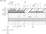
- the second switching elements 1B are mounted on the support conductor 2 (second conductive portion 2B) as shown in FIG. 8, FIG. 12, FIG. 16, FIG. 20, etc.
- the second switching elements 1B are arranged, for example, in the y direction and spaced apart from each other.
- the second switching elements 1B are each conductively joined to the support conductor 2 (second conductive portion 2B) via an intermediate joining material 19b.
- the element back surface 10b faces the support conductor 2 (second conductive portion 2B).
- the first switching elements 1A and the second switching elements 1B overlap when viewed in the x direction. Unlike this configuration, the first switching elements 1A and the second switching elements 1B do not have to overlap when viewed in the x direction.
- the semiconductor elements 1 each have a first principal surface electrode 11, a second principal surface electrode 12, a third principal surface electrode 13, and a back surface electrode 15, as shown in FIG. 8, FIG. 13, and FIG. 16.
- the configurations of the first principal surface electrode 11, the second principal surface electrode 12, the third principal surface electrode 13, and the back surface electrode 15 described below are common to all the semiconductor elements 1.
- the first principal surface electrode 11, the second principal surface electrode 12, and the third principal surface electrode 13 are provided on the element principal surface 10a.
- the first principal surface electrode 11, the second principal surface electrode 12, and the third principal surface electrode 13 are insulated by an insulating film (not shown).
- the back surface electrode 15 is provided on the element back surface 10b.
- the back surface electrode 15 covers the entire area (or substantially the entire area) of the element back surface 10b.
- the back surface electrode 15 is formed, for example, by Ag (silver) plating.
- the first principal surface electrode 11 is, for example, a gate electrode to which a drive signal (for example, a gate voltage) for driving each semiconductor element 1 is input.
- the second principal surface electrode 12 is, for example, a source electrode through which a source current flows.
- the third principal surface electrode 13 is, for example, a source sense electrode, and has the same potential as the second principal surface electrode 12.
- the third principal surface electrode 13 has the same source current as the second principal surface electrode 12.
- the back surface electrode 15 is, for example, a drain electrode through which a drain current flows.
- each semiconductor element 1 switches between a conductive state and a cut-off state in response to the drive signal.
- This operation of switching between a conductive state and a cut-off state is called a switching operation.
- a forward current flows from the back surface electrode 15 (drain electrode) to the second principal surface electrode 12 (source electrode), and in the cut-off state, this forward current does not flow.
- the semiconductor device A1 converts a first power supply voltage (e.g., a DC voltage) into a second power supply voltage (e.g., an AC voltage) by the function of each semiconductor element 1.
- the first power supply voltage is input (applied) between the power terminal 41 and the two power terminals 42, and the second power supply voltage is input (applied) to the two power terminals 43.
- the semiconductor device A1 has two thermistors 17. Each thermistor 17 is used as a sensor for detecting temperature.
- Support conductor 2 supports the multiple semiconductor elements 1 (the multiple first switching elements 1A and the multiple second switching elements 1B).
- the supporting conductor 2 is joined onto a supporting substrate 3.
- the supporting conductor 2 has, for example, a rectangular shape in a plan view.
- the support conductor 2 includes a first conductive portion 2A and a second conductive portion 2B.
- the first conductive portion 2A has a main body layer 20A, a bonding layer 21A, and a bonding layer 22A.
- the second conductive portion 2B has a main body layer 20B, a bonding layer 21B, and a bonding layer 22B.
- the main body layer 20A and the main body layer 20B are each a plate-shaped member made of metal. This metal is Cu (copper) or a Cu alloy.
- the first conductive portion 2A and the second conductive portion 2B together with the multiple power terminals 41 to 43, form a conduction path to the multiple first switching elements 1A and the multiple second switching elements 1B.
- the first conductive portion 2A and the second conductive portion 2B are each, for example, rectangular in a plan view.
- the first conductive portion 2A and the second conductive portion 2B each have, for example, a dimension in the x direction of 15 mm or more and 25 mm or less, a dimension in the y direction of 30 mm or more and 40 mm or less, and a dimension in the z direction of 1.0 mm or more and 5.0 mm or less (preferably about 2.0 mm).
- These dimensions of the first conductive portion 2A and the second conductive portion 2B are not limited to the numerical examples given above, and can be changed as appropriate according to the specifications of the semiconductor device A1.
- the first conductive portion 2A is bonded to the support substrate 3 via an intermediate bonding material 29a
- the second conductive portion 2B is bonded to the support substrate 3 via an intermediate bonding material 29b.
- a plurality of first switching elements 1A are bonded to the first conductive portion 2A via an intermediate bonding material 19a.
- a plurality of second switching elements 1B are bonded to the second conductive portion 2B via an intermediate bonding material 19b.
- the first conductive portion 2A and the second conductive portion 2B are spaced apart in the x direction as shown in Figs. 3, 8, 11, 12, and 19. In the examples shown in these figures, the first conductive portion 2A is located on the x1 side of the second conductive portion 2B.
- the first conductive portion 2A and the second conductive portion 2B overlap when viewed in the x direction.
- the support conductor 2 (each of the first conductive portion 2A and the second conductive portion 2B) has a main surface 201 and a back surface 202. As shown in Figures 11 to 22, the main surface 201 and the back surface 202 are spaced apart in the z direction. The main surface 201 faces the z2 side, and the back surface 202 faces the z1 side. The back surface 202 faces the support substrate 3.
- the semiconductor device A1 has a joint structure B11.
- the joint structure B11 is a structure in which a first switching element 1A as a first joint object and a first conductive portion 2A as a second joint object are joined via an intermediate joint material 19a.
- the intermediate bonding material 19a has a base layer 190a, a first surface layer 191a, and a second surface layer 192a.
- the base material layer 190a is mainly composed of Cu (copper).
- Configurations in which the base material layer 190a is mainly composed of Cu (copper) include configurations made of only Cu (copper), configurations in which an additive metal is added to Cu (copper), and various Cu (copper) alloys. The same applies to configurations in which "a certain member is mainly composed of a certain metal" in the following explanation.
- the thickness of the base material layer 190a is, for example, 50 ⁇ m or more and 300 ⁇ m or less.
- the first surface layer 191a is disposed on the z2 side of the base layer 190a in the z direction.
- the first surface layer 191a is solid-state bonded to the first switching element 1A.
- Solid-state bonding is a bonding method that is achieved by applying a predetermined pressure and temperature to two layers that are mainly made of the same metal and are in direct contact with each other, and includes, for example, solid-state diffusion bonding and solid-state deformation bonding.
- the first surface layer 191a is mainly made of Ag (silver).
- the first surface layer 191a is thinner than the base layer 190a.
- the thickness of the first surface layer 191a is, for example, 0.1 ⁇ m or more and 15 ⁇ m or less.
- the first switching element 1A further has a bonding layer 151.
- the bonding layer 151 corresponds to the first bonding layer in the bonding structure B11.
- the bonding layer 151 is disposed on the z1 side of the back electrode 15 in the z direction.
- the bonding layer 151 is solid-state bonded to the first surface layer 191a.
- the bonding layer 151 is mainly composed of Ag (silver).
- the thickness of the bonding layer 151 is, for example, 0.01 ⁇ m or more and 5 ⁇ m or less.
- the metal that is the main component of the first surface layer 191a and the bonding layer 151 is not limited in any way, so long as they are configured to be solid-state bonded to each other.
- the boundary between the first surface layer 191a and the bonding layer 151, which are solid-state bonded to each other, is less clear than, for example, the boundary between the base material layer 190a and the first surface layer 191a, which is the boundary between dissimilar metals.
- the boundary between the first surface layer 191a and the bonding layer 151 is barely discernible, or is only discernible due to the presence of a small gap or the like that occurs during solid-state bonding.
- the second surface layer 192a is disposed on the z1 side of the base layer 190a in the z direction.
- the second surface layer 192a is solid-state bonded to the first conductive portion 2A.
- the second surface layer 192a is mainly composed of Ag (silver).
- the second surface layer 192a is thinner than the base layer 190a.
- the thickness of the second surface layer 192a is, for example, 0.1 ⁇ m or more and 15 ⁇ m or less.
- the bonding layer 21A of the first conductive portion 2A corresponds to the second bonding layer in the bonded structure B11.
- the bonding layer 21A is disposed on the z2 side of the main body layer 20A in the z direction.
- the bonding layer 21A is solid-state bonded to the second surface layer 192a.
- the bonding layer 21A is mainly composed of Ag (silver).
- the thickness of the bonding layer 21A is, for example, 0.1 ⁇ m or more and 15 ⁇ m or less.
- the metal that is the main component of the second surface layer 192a and the bonding layer 21A is not limited in any way, so long as they are configured to be solid-state bonded to each other.
- the semiconductor device A1 has a joint structure B12.
- the joint structure B12 is a structure in which a second switching element 1B as a first joint object and a second conductive part 2B as a second joint object are joined via an intermediate joint material 19b.
- the intermediate bonding material 19b has a base layer 190b, a first surface layer 191b, and a second surface layer 192b.
- the base material layer 190b is mainly composed of Cu (copper). There are no limitations on the thickness of the base material layer 190b, and in this embodiment, the base material layer 190b is thicker than the first surface layer 191b and the second surface layer 192b. The thickness of the base material layer 190b is, for example, 50 ⁇ m or more and 300 ⁇ m or less.
- the first surface layer 191b is disposed on the z2 side of the base layer 190b in the z direction.
- the first surface layer 191b is solid-state bonded to the second switching element 1B.
- the first surface layer 191b is mainly composed of Ag (silver).
- the first surface layer 191b is thinner than the base layer 190b.
- the thickness of the first surface layer 191b is, for example, 0.1 ⁇ m or more and 15 ⁇ m or less.
- the second switching element 1B further has a bonding layer 151 similar to that of the first switching element 1A.
- the bonding layer 151 of the second switching element 1B is solid-state bonded to the first surface layer 191b.
- the metal that is the main component of the first surface layer 191b and the bonding layer 151 is not limited in any way, so long as they are configured to be solid-state bonded to each other.
- the second surface layer 192b is disposed on the z1 side of the base layer 190b in the z direction.
- the second surface layer 192b is solid-state bonded to the second conductive portion 2B.
- the second surface layer 192b is mainly composed of Ag (silver).
- the second surface layer 192b is thinner than the base layer 190b.
- the thickness of the second surface layer 192b is, for example, 0.1 ⁇ m or more and 15 ⁇ m or less.
- the bonding layer 21B of the second conductive portion 2B corresponds to the second bonding layer in the bonding structure B12.
- the bonding layer 21B is disposed on the z2 side of the main body layer 20B in the z direction.
- the bonding layer 21B is solid-state bonded to the second surface layer 192b.
- the bonding layer 21B is mainly composed of Ag (silver).
- the thickness of the bonding layer 21B is, for example, 0.1 ⁇ m or more and 15 ⁇ m or less.
- the metal that is the main component of the second surface layer 192b and the bonding layer 21B there are no limitations on the metal that is the main component of the second surface layer 192b and the bonding layer 21B, as long as they are configured to be solid-state bonded to each other.
- the support substrate 3 supports the support conductor 2.
- the support substrate 3 is, for example, a direct bonded copper (DBC) substrate.
- the support substrate 3 may be, for example, a direct bonded aluminum (DBA) substrate.
- the support substrate 3 includes an insulating layer 31, a first metal layer 32, and a second metal layer 33.
- the insulating layer 31 is made of, for example, a ceramic with excellent thermal conductivity. Examples of such ceramics include AlN (aluminum nitride), SiN (silicon nitride), Al2O3 (aluminum oxide), and ZTA (zirconia reinforced alumina).
- the insulating layer 31 may be made of an insulating resin instead of ceramic.
- the insulating layer 31 is, for example, rectangular in plan view.
- the first metal layer 32 is formed on the upper surface (surface facing the z2 side) of the insulating layer 31.
- the constituent material of the first metal layer 32 includes, for example, Cu.
- the constituent material may include Al (aluminum) instead of Cu.
- the first metal layer 32 includes a first portion 32A and a second portion 32B.
- the first portion 32A and the second portion 32B are spaced apart in the x direction.
- the first portion 32A is located on the x1 side of the second portion 32B.
- the first conductive portion 2A is joined to the first portion 32A and supports the first conductive portion 2A.
- the second portion 32B is joined to the second conductive portion 2B and supports the second conductive portion 2B.
- the first portion 32A and the second portion 32B are each, for example, rectangular in a plan view.
- the second metal layer 33 is formed on the lower surface (surface facing the z1 side) of the insulating layer 31.
- the constituent material of the second metal layer 33 is the same as the constituent material of the first metal layer 32.
- the lower surface (surface facing the z1 side) of the second metal layer 33 is exposed from the resin member 8 as shown in Figures 10 to 22.
- a heat dissipation member e.g., a heat sink
- the second metal layer 33 overlaps both the first portion 32A and the second portion 32B in a plan view.
- the joint structure B13 is a structure in which a first conductive part 2A as a first object to be joined and a supporting substrate 3 as a second object to be joined are joined via an intermediate joining material 29a.
- the intermediate bonding material 29a has a base layer 290a, a first surface layer 291a, and a second surface layer 292a.
- the base material layer 290a is mainly composed of Cu (copper). There are no limitations on the thickness of the base material layer 290a, and in this embodiment, the base material layer 290a is thicker than the first surface layer 291a and the second surface layer 292a. The thickness of the base material layer 290a is, for example, 50 ⁇ m or more and 300 ⁇ m or less.
- the first surface layer 291a is disposed on the z2 side of the base layer 290a in the z direction.
- the first surface layer 291a is solid-state bonded to the first conductive portion 2A.
- the first surface layer 291a is mainly composed of Ag (silver).
- Ag silver
- the thickness of the first surface layer 291a is, for example, 0.1 ⁇ m or more and 15 ⁇ m or less.
- the bonding layer 22A of the first conductive portion 2A corresponds to the first bonding layer in the bonding structure B13.
- the bonding layer 22A is disposed on the z1 side of the main body layer 20A in the z direction.
- the bonding layer 22A is solid-state bonded to the first surface layer 291a.
- the bonding layer 22A is mainly composed of Ag (silver).
- the thickness of the bonding layer 22A is, for example, 0.1 ⁇ m or more and 15 ⁇ m or less.
- the metal that is the main component of the first surface layer 291a and the bonding layer 22A is not limited in any way, so long as they are configured to be solid-state bonded to each other.
- the second surface layer 292a is disposed on the z1 side of the base layer 290a in the z direction.
- the second surface layer 292a is solid-state bonded to the support substrate 3.
- the second surface layer 292a is mainly composed of Ag (silver).
- the second surface layer 292a is thinner than the base layer 290a.
- the thickness of the second surface layer 292a is, for example, 0.1 ⁇ m or more and 15 ⁇ m or less.
- the support substrate 3 of this embodiment further includes a bonding layer 321A.
- the bonding layer 321A corresponds to the second bonding layer in the bonded structure B13.
- the bonding layer 321A is disposed on the z2 side of the first portion 32A in the z direction.
- the bonding layer 321A is solid-state bonded to the second surface layer 292a.
- the bonding layer 321A is mainly composed of Ag (silver).
- the thickness of the bonding layer 321A is, for example, 0.1 ⁇ m or more and 15 ⁇ m or less.
- the semiconductor device A1 has a joint structure B14.
- the joint structure B14 is a structure in which the second conductive part 2B as the first joint object and the support substrate 3 as the second joint object are joined via an intermediate joint material 29b.
- the intermediate bonding material 29b has a base layer 290b, a first surface layer 291b, and a second surface layer 292b.
- the base material layer 290b is mainly composed of Cu (copper). There are no limitations on the thickness of the base material layer 290b, and in this embodiment, the base material layer 290b is thicker than the first surface layer 291b and the second surface layer 292b. The thickness of the base material layer 290b is, for example, 50 ⁇ m or more and 300 ⁇ m or less.
- the first surface layer 291b is disposed on the z2 side of the base layer 290b in the z direction.
- the first surface layer 291b is solid-state bonded to the second switching element 1B.
- the first surface layer 291b is mainly composed of Ag (silver).
- the first surface layer 291b is thinner than the base layer 290b.
- the thickness of the first surface layer 291b is, for example, 0.1 ⁇ m or more and 15 ⁇ m or less.
- the bonding layer 22B of the second conductive portion 2B corresponds to the first bonding layer in the bonding structure B14.
- the bonding layer 22B is disposed on the z1 side of the main body layer 20B in the z direction.
- the bonding layer 22B is solid-state bonded to the first surface layer 291b.
- the bonding layer 22B is mainly composed of Ag (silver).
- the thickness of the bonding layer 22B is, for example, 0.1 ⁇ m or more and 15 ⁇ m or less.
- the second surface layer 292b is disposed on the z1 side of the base layer 290b in the z direction.
- the second surface layer 292b is solid-state bonded to the support substrate 3.
- the second surface layer 292b is mainly composed of Ag (silver).
- the second surface layer 292b is thinner than the base layer 290b.
- the thickness of the second surface layer 292b is, for example, 0.1 ⁇ m or more and 15 ⁇ m or less.
- the support substrate 3 of this embodiment further includes a bonding layer 321B.
- the bonding layer 321B corresponds to the second bonding layer in the bonded structure B14.
- the bonding layer 321B is disposed on the z2 side of the second portion 32B in the z direction.
- the bonding layer 321B is solid-state bonded to the second surface layer 292b.
- the bonding layer 321B is mainly composed of Ag (silver).
- the thickness of the bonding layer 321B is, for example, 0.1 ⁇ m or more and 15 ⁇ m or less.
- Each of the power terminals 41 to 43 is made of a plate-shaped metal plate.
- the metal plate is made of, for example, Cu or a Cu alloy.
- the semiconductor device A1 includes one power terminal 41, two power terminals 42 and two power terminals 43.
- the first power supply voltage is applied between the power terminal 41 and the two power terminals 42.
- the power terminal 41 is, for example, a terminal (P terminal) connected to the positive pole of a DC power supply
- the two power terminals 42 are, for example, terminals (N terminals) connected to the negative pole of a DC power supply.
- the power terminal 41 may be an N terminal and the two power terminals 42 may be P terminals.
- the wiring inside the package may be changed appropriately in accordance with the change in the polarity of the terminals.
- the second power supply voltage is applied to each of the two power terminals 43.
- the two power terminals 43 are output terminals that output a voltage (the second power supply voltage) converted by the switching operations of the first switching elements 1A and the second switching elements 1B.
- Each of the power terminals 41 to 43 includes a portion covered by the resin member 8 and a portion exposed from the resin member 8.
- the power terminal 41 is formed integrally with the first conductive portion 2A as shown in Figures 8, 12 and 19. Alternatively, the power terminal 41 may be separated from the first conductive portion 2A and conductively joined to the first conductive portion 2A. As shown in Figure 8, the power terminal 41 is located on the x2 side of the multiple semiconductor elements 1 and the first conductive portion 2A (support conductor 2).
- the insulating layer 31 is conductive to the first conductive portion 2A and is conductive to the back electrodes 15 (drain electrodes) of the multiple first switching elements 1A via the first conductive portion 2A.
- the power terminal 41 is an example of a "first power terminal.”
- the two power terminals 42 are each spaced apart from the first conductive portion 2A, as shown in Figures 8 and 11, etc.
- a second conductive member 72 is joined to each of the two power terminals 42.
- each of the two power terminals 42 is located on the x2 side of the multiple semiconductor elements 1 and the first conductive portion 2A (support conductor 2).
- Each of the two power terminals 42 is conductive to the second conductive member 72, and is conductive to the second principal surface electrodes 12 (source electrodes) of the multiple second switching elements 1B via the second conductive member 72.
- Each power terminal 42 is an example of a "second power terminal.”
- the power terminal 41 and the two power terminals 42 each protrude from the resin member 8 toward the x2 side.
- the power terminal 41 and the two power terminals 42 are spaced apart from each other.
- the two power terminals 42 are located on opposite sides of the power terminal 41 in the y direction. As can be seen from Figures 6, 7, and 9, the power terminal 41 and the two power terminals 42 overlap each other when viewed in the y direction.
- the two power terminals 43 are each formed integrally with the second conductive portion 2B, for example, as shown in FIG. 8 and FIG. 11. Alternatively, the two power terminals 43 may be separated from the second conductive portion 2B and conductively joined to the second conductive portion 2B. As shown in FIG. 8, the two power terminals 43 are each located on the x1 side of the semiconductor elements 1 and the second conductive portion 2B (support conductor 2). Each power terminal 43 is conductive to the first conductive portion 2A and is conductive to the back electrode 15 (drain) of each second switching element 1B via the first conductive portion 2A.
- the number of power terminals 43 is not limited to two, and may be, for example, one, or three or more. For example, when there is one power terminal 43, it is desirable that it is connected to the center portion in the y direction of the second conductive portion 2B.
- Each power terminal 43 is an example of a "third power terminal".
- Each of the control terminals 44 is a pin-shaped terminal for controlling the driving of the semiconductor elements 1 (the first switching elements 1A and the second switching elements 1B).
- Each of the control terminals 44 is, for example, a press-fit terminal.
- the dimension of each of the control terminals 44 in the z direction is, for example, 10 mm or more and 30 mm or less (15.8 mm in one example).
- the dimension of the control terminal 44 in the z direction is the length from the lower end (the end on the z1 side) of a holder 441 described later to the upper end (the end on the z2 side) of a metal pin 442 described later.
- the control terminals 44 include a plurality of first control terminals 45 and a plurality of second control terminals 46.
- the first control terminals 45 are used to control the first switching elements 1A.
- the second control terminals 46 are used to control the second switching elements 1B.
- a plurality of first control terminals 45 The multiple first control terminals 45 are arranged at intervals in the y direction, as shown in Fig. 4.
- the multiple first control terminals 45 are fixed to the signal board 5 (first signal board 5A).
- the multiple first control terminals 45 are located between the multiple first switching elements 1A and the multiple power terminals 41, 42 in the x direction, as shown in Figs. 5 to 7 and 12.
- the multiple first control terminals 45 include a first drive terminal 45A and multiple first detection terminals 45B to 45E, as shown in Figs. 1 and 4.
- the first drive terminal 45A is a terminal (gate terminal) for inputting a drive signal to the multiple first switching elements 1A.
- a first drive signal for driving the multiple first switching elements 1A is input to the first drive terminal 45A (for example, a gate voltage is applied).
- the first detection terminal 45B is a terminal (source sense terminal) for detecting the source signals of the multiple first switching elements 1A.
- the first detection terminal 45B outputs a first detection signal for detecting the conductive state of the multiple first switching elements 1A.
- the first detection terminal 45B detects a voltage (voltage corresponding to the source current) applied to the second principal surface electrode 12 (source electrode) of the first switching element 1A as the first detection signal.
- the first detection terminal 45C and the first detection terminal 45D are terminals that are each electrically connected to one of the two thermistors 17.
- the one thermistor 17 is mounted on the first signal board 5A, which will be described later.
- the first detection terminal 45E is a terminal (drain sense terminal) for detecting the drain signals of the multiple first switching elements 1A.
- the first detection terminal 45E detects the voltage (voltage corresponding to the drain current) applied to each back electrode 15 (drain electrode) of the multiple first switching elements 1A.
- a plurality of second control terminals 46 The second control terminals 46 are arranged at intervals in the y direction, as shown in Fig. 4.
- the second control terminals 46 are fixed to the signal board 5 (second signal board 5B).
- the second control terminals 46 are located between the second switching elements 1B and the power terminals 43 in the x direction, as shown in Figs. 5 to 7 and 12.
- the second control terminals 46 include a second drive terminal 46A and a plurality of second detection terminals 46B to 46E, as shown in Figs. 1 and 4.
- the second drive terminal 46A is a terminal (gate terminal) for inputting a drive signal to the multiple second switching elements 1B.
- a second drive signal for driving the multiple second switching elements 1B is input to the second drive terminal 46A (for example, a gate voltage is applied).
- the second detection terminal 46B is a terminal (source sense terminal) for detecting the source signals of the multiple second switching elements 1B.
- the multiple second detection terminals 46B output second detection signals for detecting the conductive state of the multiple second switching elements 1B.
- the second detection terminal 46B detects a voltage (voltage corresponding to the source current) applied to the second principal surface electrode 12 (source electrode) of the second switching element 1B as the second detection signal.
- the second detection terminal 46C and the second detection terminal 46D are terminals that are each conductive to the other of the two thermistors 17.
- the other thermistor 17 is mounted on the second signal board 5B, which will be described later.
- the second detection terminal 46E is a terminal (drain sense terminal) for detecting the drain signals of the multiple second switching elements 1B.
- the second detection terminal 46E detects the voltage (voltage corresponding to the drain current) applied to each back electrode 15 (drain electrode) of the multiple second switching elements 1B.
- a plurality of control terminals 44 Each of the plurality of control terminals 44 (the plurality of first control terminals 45 and the plurality of second control terminals 46 ) includes a holder 441 and a metal pin 442 .
- the holder 441 is made of a conductive material. As shown in Figures 13 and 16, the holder 441 is bonded to the signal board 5 (first metal layer 52 described below) via a conductive bonding material 449.
- the holder 441 includes a cylindrical portion, an upper end flange, and a lower end flange. The upper end flange is connected to the upper end of the cylindrical portion in the z direction (z2 side), and the lower end flange is connected to the lower end of the cylindrical portion in the z direction (z1 side).
- a metal pin 442 is inserted through at least the upper end flange and the cylindrical portion of the holder 441.
- the holder 441 is covered with a resin member 8.
- the metal pin 442 is a rod-shaped member extending in the z direction.
- the metal pin 442 is supported by being pressed into the holder 441.
- the metal pin 442 is electrically connected to the signal board 5 (first metal layer 52 described below) at least via the holder 441.
- the metal pin 442 is electrically connected to the signal board 5 even via the conductive bonding material 449.
- the signal board 5 supports a plurality of control terminals 44.
- the signal board 5 is interposed between the support conductor 2 and each control terminal 44 in the z direction.
- the thickness (dimension in the thickness direction z) of the signal board 5 is, for example, 0.5 mm or more and 1.0 mm or less.
- the dimension in the thickness direction z of each control terminal 44 is 20 times or more and 30 times or less the thickness (dimension in the thickness direction z) of the signal board 5.
- the signal board 5 includes a first signal board 5A and a second signal board 5B.
- the first signal board 5A is disposed on the first conductive portion 2A and supports a plurality of first control terminals 45. As shown in Figures 12, 13, and 19, the first signal board 5A is adhered to the first conductive portion 2A via an adhesive layer 6 (first adhesive body 6A).
- the second signal board 5B is disposed on the second conductive portion 2B and supports a plurality of second control terminals 46. As shown in Figures 12, 16 and 19, the second signal board 5B is adhered to the second conductive portion 2B via an adhesive layer 6 (second adhesive body 6B).
- the signal substrate 5 (each of the first signal substrate 5A and the second signal substrate 5B) is formed of, for example, a DBC substrate.
- the signal substrate 5 has an insulating substrate 51, a first metal layer 52, and a second metal layer 53 stacked on top of each other. Unless otherwise specified, the insulating substrate 51, the first metal layer 52, and the second metal layer 53 described below are common to the first signal substrate 5A and the second signal substrate 5B.
- the insulating substrate 51 is made of, for example, ceramic. Examples of such ceramics include AlN, SiN, and Al2O3.
- the insulating substrate 51 is, for example, rectangular in plan view. As shown in Figures 13 and 16, the insulating substrate 51 has a principal surface 51a and a rear surface 51b. The principal surface 51a and the rear surface 51b are spaced apart in the z direction. The principal surface 51a faces the z2 side, and the rear surface 51b faces the z1 side. The rear surface 51b faces the supporting conductor 2.
- the second metal layer 53 is formed on the back surface 51b of the insulating substrate 51, as shown in Figures 13 and 16.
- the second metal layer 53 is adhered to the support conductor 2 via an adhesive layer 6.
- the second metal layer 53 of the first signal substrate 5A is adhered to the first conductive portion 2A via a first adhesive 6A described below, and the second metal layer 53 of the second signal substrate 5B is adhered to the second conductive portion 2B via a second adhesive 6B.
- the second metal layer 53 is made of, for example, Cu or a Cu alloy.
- the second metal layer 53 is an example of a "metal layer".
- the first metal layer 52 is formed on the main surface 51a of the insulating substrate 51, as shown in Figs. 13 and 16.
- the multiple control terminals 44 are each provided on the first metal layer 52.
- the first metal layer 52 of the first signal substrate 5A has multiple first control terminals 45 provided thereon, and the first metal layer 52 of the second signal substrate 5B has multiple second control terminals 46 provided thereon.
- the first metal layer 52 is made of, for example, Cu or a Cu alloy. As shown in Fig. 8, the first metal layer 52 includes multiple wiring layers 521-526. The multiple wiring layers 521-526 are spaced apart and insulated from each other.
- the wiring layer 521 has a plurality of wires 73 bonded thereto, and is electrically connected to the first principal surface electrodes 11 (gate electrodes) of each semiconductor element 1 via each wire 73.
- the wiring layer 521 of the first signal substrate 5A is electrically connected to the first principal surface electrodes 11 of each first switching element 1A via each wire 73.
- the wiring layer 521 of the second signal substrate 5B is electrically connected to the first principal surface electrodes 11 of each second switching element 1B via each wire 73.
- the wiring layer 526 has a plurality of wires 75 bonded thereto, and is electrically connected to the wiring layer 521 via each wire 75.
- the wiring layer 526 of the first signal board 5A is electrically connected to the first principal surface electrodes 11 (gate electrodes) of each first switching element 1A via each wire 75, the wiring layer 521 of the first signal board 5A, and each wire 73.
- the wiring layer 526 of the second signal board 5B is electrically connected to the first principal surface electrodes 11 (gate electrodes) of each second switching element 1B via each wire 75, the wiring layer 521 of the second signal board 5B, and each wire 73.
- the first drive terminal 45A is bonded to the wiring layer 526 of the first signal board 5A
- the second drive terminal 46A is bonded to the wiring layer 526 of the second signal board 5B.
- the wiring layer 522 has a plurality of wires 74 bonded thereto, and is electrically connected to the third principal surface electrodes 13 (source sense electrodes) of the respective semiconductor elements 1 via the respective wires 74.
- the wiring layer 522 of the first signal board 5A is electrically connected to the third principal surface electrodes 13 (source sense electrodes) of the respective first switching elements 1A via the respective wires 74.
- the wiring layer 522 of the second signal board 5B is electrically connected to the third principal surface electrodes 13 (source sense electrodes) of the respective second switching elements 1B via the respective wires 74.
- the first detection terminal 45B is bonded to the wiring layer 522 of the first signal board 5A
- the second detection terminal 46B is bonded to the wiring layer 522 of the second signal board 5B.
- the wiring layer 523 and the wiring layer 524 are bonded to a thermistor 17.
- the first detection terminal 45C and the first detection terminal 45D are bonded to the wiring layer 523 and the wiring layer 524 of the first signal board 5A, respectively.
- the second detection terminal 46C and the second detection terminal 46D are bonded to the wiring layer 523 and the wiring layer 524 of the second signal board 5B, respectively.
- the wiring layer 525 has wires 76 bonded thereto, and is electrically connected to the support conductor 2 via the wires 76. As shown in FIG. 8, the wiring layer 525 of the first signal board 5A is electrically connected to the first conductive portion 2A via the wires 76. The wiring layer 525 of the second signal board 5B is electrically connected to the second conductive portion 2B via the wires 76. The first detection terminal 45E is bonded to the wiring layer 525 of the first signal board 5A. The second detection terminal 46E is bonded to the wiring layer 525 of the second signal board 5B.
- the signal board 5 may be a printed circuit board such as a glass epoxy board instead of a DBC board. At least the above wiring layers 521 to 526 are formed on the printed circuit board.
- Adhesive layer 6 bonds the signal substrate 5 and the supporting conductor 2.
- the adhesive layer 6 is interposed between the signal substrate 5 and the supporting conductor 2 in the z direction.
- the adhesive layer 6 overlaps the signal substrate 5 in a plan view.
- the thickness (dimension in the z direction) of the adhesive layer 6 is, for example, not less than 20 ⁇ m and not more than 200 ⁇ m (85 ⁇ m in one example).
- the adhesive layer 6 includes a first adhesive body 6A and a second adhesive body 6B.
- the first adhesive body 6A bonds the first signal board 5A and the first conductive portion 2A.
- the first adhesive body 6A is interposed between the first signal board 5A and the first conductive portion 2A, and overlaps the first signal board 5A in a planar view.
- the second adhesive body 6B bonds the second signal board 5B and the second conductive portion 2B. It is interposed between the second signal board 5B and the second conductive portion 2B, and overlaps the second signal board 5B in a planar view.
- the adhesive layer 6 (each of the first adhesive body 6A and the second adhesive body 6B) includes an insulating layer 61 and a pair of adhesive layers 62, 63, as shown in Figures 13 and 16.
- the insulating layer 61 and the pair of adhesive layers 62, 63 described below are common to both the first adhesive body 6A and the second adhesive body 6B, unless otherwise specified.
- the insulating layer 61 is made of a resin material.
- the resin material is preferably, for example, polyimide.
- the insulating layer 61 of the first adhesive 6A electrically insulates the first signal board 5A from the first conductive part 2A
- the insulating layer 61 of the second adhesive 6B electrically insulates the second signal board 5B from the second conductive part 2B.
- the insulating layer 61 is, for example, a film.
- the insulating layer 61 may be a sheet or plate instead of a film. In this disclosure, a sheet is as soft as a film, but is thicker than a film. A plate is harder and less flexible than a film or sheet, and is thicker than a sheet.
- the definitions of film, sheet, and plate are not limited to these, and may be changed as appropriate according to conventional classifications.
- the thickness (dimension in the thickness direction z) of the insulating layer 61 is 0.1% to 1.0% of the dimension in the thickness direction z of each control terminal 44.
- the thickness of the insulating layer 61 (dimension in the thickness direction z) is 20% or more and 75% or less of the thickness of the adhesive layer 6 (dimension in the thickness direction z).
- the thickness of the insulating layer 61 (dimension in the z direction) is, for example, 10 ⁇ m or more and 150 ⁇ m or less (25 ⁇ m in one example).
- the insulating layer 61 includes a principal surface 61a and a rear surface 61b.
- the principal surface 61a and the rear surface 61b are spaced apart in the z direction.
- the principal surface 61a faces the z2 side (upward in the z direction), and the rear surface 61b faces the z1 side (downward in the z direction).
- the pair of adhesive layers 62, 63 are formed on both sides of the insulating layer 61 in the z direction.
- Each of the pair of adhesive layers 62, 63 is made of, for example, a silicone-based adhesive or an acrylic-based adhesive.
- the thickness (dimension in the thickness direction z) of each of the pair of adhesive layers 62, 63 is 10% to 150% of the thickness (dimension in the thickness direction z) of the insulating layer 61.
- the thickness (dimension in the z direction) of each of the pair of adhesive layers 62, 63 is, for example, 5 ⁇ m to 50 ⁇ m (30 ⁇ m in one example).
- the adhesive layer 62 is formed on the main surface 61a as shown in Figures 13 and 16.
- the adhesive layer 62 is interposed between the insulating layer 61 and the signal board 5 in the z direction.
- the adhesive layer 62 of the first adhesive body 6A is interposed between the insulating layer 61 of the first adhesive body 6A and the first signal board 5A in the z direction, and the adhesive layer 62 of the second adhesive body 6B is interposed between the insulating layer 61 of the second adhesive body 6B and the second signal board 5B in the z direction.
- the adhesive layer 63 is formed on the back surface 61b as shown in Figures 13 and 16.
- the adhesive layer 63 is interposed between the insulating layer 61 and the support conductor 2 in the z direction.
- the adhesive layer 63 of the first adhesive body 6A is interposed between the insulating layer 61 of the first adhesive body 6A and the first conductive portion 2A in the z direction, and the adhesive layer 63 of the second adhesive body 6B is interposed between the insulating layer 61 of the second adhesive body 6B and the second conductive portion 2B.
- the adhesive layer 6 of the present disclosure is, for example, something like a double-sided adhesive tape.
- the adhesive layer 6 is attached to, for example, a signal board 5 to which a plurality of control terminals 44 are bonded, and is then attached to the support conductor 2.
- the adhesive layer 6 does not have to be a double-sided adhesive tape, and does not include adhesives that temporarily become molten, such as solder, when bonding two components together.
- the adhesive layer 6 may be anything that can bond two components together without becoming molten.
- First conductive member 71 and second conductive member 72 The first conductive member 71 and the second conductive member 72, together with the support conductor 2, constitute a path of a main circuit current switched by the plurality of semiconductor elements 1 (the plurality of first switching elements 1A and the plurality of second switching elements 1B).
- the first conductive member 71 and the second conductive member 72 are spaced from the respective main surfaces 201 of the first conductive portion 2A and the second conductive portion 2B on the z2 side and overlap the respective main surfaces 201 in a plan view.
- the first conductive member 71 and the second conductive member 72 are each made of, for example, a metal plate material.
- the metal is, for example, Cu or a Cu alloy.
- the first conductive member 71 and the second conductive member 72 are appropriately bent.
- the first conductive member 71 provides electrical continuity between the multiple first switching elements 1A and the second conductive portion 2B. As shown in Figures 5 and 8, the first conductive member 71 is connected to the second principal surface electrode 12 (source electrode) of each first switching element 1A and the second conductive portion 2B, and provides electrical continuity between the second principal surface electrode 12 of each first switching element 1A and the second conductive portion 2B. The first conductive member 71 forms a path for the main circuit current switched by the multiple first switching elements 1A. As shown in Figures 5, 8 and 12, the first conductive member 71 includes a main portion 711, multiple first connection ends 712, and multiple second connection ends 713.
- the main portion 711 is located between the multiple first switching elements 1A and the second conductive portion 2B in the x direction.
- the main portion 711 is a band-shaped portion extending in the y direction.
- the main portion 711 is located on the z2 side of the multiple first connection ends 712 and the multiple second connection ends 713.
- the main portion 711 has multiple openings 711a formed therein.
- Each of the multiple openings 711a is a through hole that penetrates the first conductive member 71 (main portion 711) in the z direction.
- the multiple openings 711a are arranged at intervals in the y direction.
- the multiple openings 711a do not overlap the second conductive member 72 in a planar view.
- the multiple openings 711a are formed to facilitate the flow of the resin material between the upper side (z2 side) and the lower side (z1 side) near the main portion 711 (first conductive member 71) when injecting the fluid resin material to form the resin member 8.
- the shape of the main portion 711 is not limited to this configuration, and for example, the openings 711a do not have to be formed.
- the first connection ends 712 and the second connection ends 713 are each connected to the main portion 711 and are arranged opposite the first switching elements 1A. As shown in FIG. 12, the first connection ends 712 are each joined to the second main surface electrodes 12 of the first switching elements 1A via a conductive bonding material 719. The second connection ends 713 are each joined to the second conductive portion 2B via a conductive bonding material 719.
- the conductive bonding material 719 is, for example, solder, a metal paste material, or a sintered metal.
- an opening 712a is formed in each first connection end 712.
- each opening 712a is formed so as to overlap the center of each first switching element 1A in a plan view.
- Each opening 712a is, for example, a through hole that penetrates each first connection end 712 in the z direction, as shown in FIG. 12, FIG. 13, and FIG. 21.
- the opening 712a is used, for example, when positioning the first conductive member 71 relative to the supporting conductor 2.
- the multiple first connection ends 712 and the multiple second connection ends 713 are each connected to one another by the main portion 711, but instead of this configuration, the main portion 711 may be divided into multiple portions, and the divided portions may connect each of the multiple first connection ends 712 and each of the multiple second connection ends 713.
- the configuration may include one first conductive member 71 for each of the multiple first switching elements 1A.
- the second conductive member 72 is connected to the second main surface electrode 12 (source electrode) of each second switching element 1B and the multiple power terminals 42, and electrically connects the second main surface electrode 12 of each second switching element 1B and each power terminal 42.
- the second conductive member 72 forms a path for a main circuit current switched by the multiple second switching elements 1B.
- the second conductive member 72 has a maximum dimension in the x direction of, for example, 25 mm or more and 40 mm or less, and a maximum dimension in the y direction of, for example, 30 mm or more and 45 mm or less.
- the second conductive member 72 includes a pair of first wiring portions 721, second wiring portions 722, third wiring portions 723 and fourth wiring portions 724.
- each of the pair of first wiring parts 721 is connected to one of the pair of power terminals 42, and the other of the pair of first wiring parts 721 is connected to the other of the pair of power terminals 42.
- each of the pair of first wiring parts 721 is a strip extending in the x direction in a plan view.
- the pair of first wiring parts 721 are spaced apart in the y direction and arranged parallel (or approximately parallel).
- each of the pair of first wiring parts 721 includes a first end 721a.
- Each first end 721a is an end of each first wiring part 721 on the x2 side.
- each first end 721a is located on the z1 side relative to other parts of each first wiring part 721.
- each first end 721a is joined to each of the pair of power terminals 42 via a conductive bonding material 729.
- the conductive bonding material 729 is, for example, solder, metal paste, or sintered metal.
- multiple notches are formed in each first wiring portion 721.
- the multiple notches formed in each first wiring portion 721 are, for example, semicircular in plan view, and overlap the support conductor 2 in plan view.
- the second wiring portion 722 is connected to both of the pair of first wiring portions 721 as shown in FIG. 5.
- the second wiring portion 722 is sandwiched between the pair of first wiring portions 721 in the y direction.
- the second wiring portion 722 is a strip extending in the y direction in a plan view.
- the second wiring portion 722 overlaps the multiple second switching elements 1B as shown in FIG. 5.
- the second wiring portion 722 is connected to each second switching element 1B.
- the second wiring portion 722 has multiple concave regions 722a. As shown in FIG. 20, each of the multiple concave regions 722a protrudes downward in the z direction (to the z1 side) further than other parts of the second wiring portion 722. As shown in FIG.
- each concave region 722a of the second wiring portion 722 and each second principal surface electrode 12 (source electrode) of the multiple second switching elements 1B are joined via a conductive bonding material 729.
- a slit is formed in each recessed region 722a. The slit is located at the center of each recessed region 722a in the y direction and extends in the x direction. Each recessed region 722a is made up of two parts separated in the y direction by the slit. Note that a slit does not necessarily have to be formed in each recessed region 722a.
- the third wiring portion 723 is connected to both of the pair of first wiring portions 721 as shown in FIG. 5.
- the first wiring portion 721 is sandwiched between the pair of first wiring portions 721 in the y direction.
- the third wiring portion 723 is a strip extending in the y direction in a plan view.
- the third wiring portion 723 is spaced apart from the second wiring portion 722 in the x direction.
- the third wiring portion 723 is arranged parallel (or approximately parallel) to the second wiring portion 722. As shown in FIG. 5, the third wiring portion 723 overlaps the multiple first switching elements 1A in a plan view.
- the third wiring portion 723 is located above (on the z2 side) each of the first connection ends 712 of the first conductive member 71 in the z direction.
- the third wiring portion 723 overlaps the first connection ends 712 in a plan view.
- each of the multiple fourth wiring parts 724 is connected to both the second wiring part 722 and the third wiring part 723.
- Each of the fourth wiring parts 724 is sandwiched between the second wiring part 722 and the third wiring part 723 in the x direction.
- Each of the fourth wiring parts 724 is a strip extending in the x direction in a plan view.
- the multiple fourth wiring parts 724 are spaced apart in the y direction and arranged parallel (or approximately parallel) in a plan view.
- the multiple fourth wiring parts 724 are arranged parallel (or approximately parallel) to a pair of first wiring parts 721.
- each of the multiple fourth wiring parts 724 in the x direction is connected to a portion of the third wiring part 723 that overlaps between two first switching elements 1A adjacent in the y direction in a plan view.
- the other end of each of the multiple fourth wiring parts 724 in the x direction is connected to a portion of the second wiring part 722 that overlaps between two second switching elements 1B adjacent in the y direction in a plan view.
- Each of the multiple fourth wiring parts 724 overlaps, for example, the first conductive member 71 (main part 711).
- Each of the wires 73 to 76 is, for example, a bonding wire, and provides electrical continuity between two parts spaced apart from each other.
- the material of each of the wires 73 to 76 includes, for example, any one of Au (gold), Al, and Cu.
- the multiple wires 73 are bonded to the wiring layer 521 and the first principal surface electrodes 11 (gate electrodes) of each semiconductor element 1, providing electrical continuity between them. As shown in FIG. 8, the multiple wires 73 include wires bonded to the wiring layer 521 of the first signal substrate 5A and the first principal surface electrodes 11 of each first switching element 1A, and wires bonded to the wiring layer 521 of the second signal substrate 5B and the first principal surface electrodes 11 of each second switching element 1B.
- the multiple wires 74 are bonded to the wiring layer 522 and the third principal surface electrodes 13 (source sense electrodes) of each semiconductor element 1, and provide electrical continuity between them. As shown in FIG. 8, the multiple wires 74 include those bonded to the wiring layer 522 of the first signal substrate 5A and the third principal surface electrodes 13 of each first switching element 1A, and those bonded to the wiring layer 522 of the second signal substrate 5B and the third principal surface electrodes 13 of each second switching element 1B. In a configuration in which each semiconductor element 1 does not have a third principal surface electrode 13, the multiple wires 74 are bonded to each second principal surface electrode 12 instead of each third principal surface electrode 13.
- the multiple wires 75 are bonded to the wiring layer 521 and the wiring layer 526, and provide electrical continuity between them. As shown in FIG. 8, the multiple wires 75 include wires bonded to the wiring layer 521 and the wiring layer 526 of the first signal board 5A, and wires bonded to the wiring layer 521 and the wiring layer 526 of the second signal board 5B.
- the multiple wires 76 are bonded to the wiring layer 525 and the support conductor 2, providing electrical continuity between them. As shown in FIG. 8, the multiple wires 76 include wires bonded to the wiring layer 525 and the first conductive portion 2A of the first signal board 5A, and wires bonded to the wiring layer 525 and the second conductive portion 2B of the second signal board 5B.
- the resin member 8 is a sealing material that protects the semiconductor elements 1 (the first switching elements 1A and the second switching elements 1B).
- the resin member 8 covers the semiconductor elements 1 (the first switching elements 1A and the second switching elements 1B), the support conductor 2 (the first conductive portion 2A and the second conductive portion 2B), the support substrate 3 (excluding the lower surface of the second metal layer 33), a portion of each of the power terminals 41 to 43, a portion of each of the control terminals 44, the signal substrate 5 (the first signal substrate 5A and the second signal substrate 5B), the adhesive layer 6 (the first adhesive body 6A and the second adhesive body 6B), the first conductive member 71, the second conductive member 72, and the wires 73 to 76.
- the resin member 8 is made of, for example, a black epoxy resin.
- the resin member 8 is formed, for example, by molding.
- Resin member 8 has, for example, a dimension in the x direction of about 35 mm to 60 mm, a dimension in the y direction of about 35 mm to 50 mm, and a dimension in the z direction of about 4 mm to 15 mm. These dimensions are the sizes of the maximum portions along each direction.
- Resin member 8 has a resin main surface 81, a resin back surface 82, and a plurality of resin side surfaces 831 to 834.
- the resin main surface 81 and the resin back surface 82 are spaced apart in the z direction as shown in Figures 6, 7, 9, 11, 12, and 19 to 22.
- the resin main surface 81 faces the z2 side, and the resin back surface 82 faces the z1 side.
- a plurality of control terminals 44 protrude from the resin main surface 81.
- the resin back surface 82 is a frame surrounding the lower surface of the second metal layer 33 of the support substrate 3 in a plan view. The lower surface of the second metal layer 33 is exposed from the resin back surface 82 and is, for example, flush with the resin back surface 82.
- the plurality of resin side surfaces 831 to 834 are each connected to both the resin main surface 81 and the resin back surface 82, and are sandwiched between them in the z direction. As shown in Figure 4 and other figures, the resin side surface 831 and the resin side surface 832 are spaced apart in the x direction. Resin side surface 831 faces the x1 side, and resin side surface 832 faces the x2 side. Two power terminals 43 protrude from resin side surface 831, and multiple power terminals 41, 42 protrude from resin side surface 832. As shown in FIG. 4 and other figures, resin side surface 833 and resin side surface 834 are spaced apart in the y direction. Resin side surface 833 faces the y1 side, and resin side surface 834 faces the y2 side.
- a plurality of recesses 832a are formed on the resin side surface 832.
- Each recess 832a is a portion recessed in the x direction in plan view.
- the plurality of recesses 832a include those formed between the power terminal 41 and one of the two power terminals 42, and those formed between the power terminal 41 and the other of the two power terminals 42.
- the plurality of recesses 832a are provided to increase the creepage distance along the resin side surface 832 between the power terminal 41 and one of the two power terminals 42, and the creepage distance along the resin side surface 832 between the power terminal 41 and the other of the two power terminals 42.
- the resin member 8 has a plurality of first protrusions 851, a plurality of second protrusions 852, and a resin void portion 86.
- Each of the first protrusions 851 protrudes in the z direction from the resin main surface 81.
- the first protrusions 851 are arranged near the four corners of the resin member 8 in a plan view.
- a first protrusion end surface 851a is formed at the tip (the end on the z2 side) of each of the first protrusions 851.
- Each of the first protrusion end surfaces 851a of the first protrusions 851 is parallel (or approximately parallel) to the resin main surface 81.
- the first protrusion end surfaces 851a are arranged on the same plane (x-y plane).
- Each of the first protrusions 851 is, for example, a hollow truncated cone with a bottom.
- the first protrusions 851 are used as spacers when the semiconductor device A1 is mounted on a control circuit board or the like.
- the control circuit board is included in an apparatus that uses the power generated by the semiconductor device A1.
- each of the first protrusions 851 has a recess 851b and an inner wall surface 851c formed in the recess 851b.
- the shape of each first protrusion 851 may be columnar, and is preferably cylindrical.
- the shape of the recess 851b is preferably cylindrical, and the inner wall surface 851c is preferably a single perfect circle in plan view.
- the semiconductor device A1 may be fixed to the control circuit board or the like by a method such as screwing.
- a female screw thread may be formed on the inner wall surface 851c of the recess 851b of each first protrusion 851.
- An insert nut or the like may be embedded in the recess 851b of each first protrusion 851.
- the multiple second protrusions 852 protrude in the z direction from the resin main surface 81.
- the multiple second protrusions 852 overlap the multiple control terminals 44 in a plan view.
- Each metal pin 442 of the multiple control terminals 44 protrudes from each second protrusion 852.
- Each second protrusion 852 is frustum-shaped.
- Each second protrusion 852 covers the holder 441 and a portion of the metal pin 442 in each control terminal 44.
- the resin void portion 86 extends in the z direction from the resin main surface 81 to each main surface 201 of the first conductive portion 2A and the second conductive portion 2B.
- the resin void portion 86 is tapered, and the cross-sectional area in a plane perpendicular to the z direction decreases from the resin main surface 81 to each main surface 201 in the z direction.
- the resin void portion 86 is formed during molding of the resin member 8, and is a portion where the resin member 8 is not formed during this molding.
- the resin voids 86 are formed, for example, when the resin member 8 is molded, because the pressing member occupies the resin member 8 and prevents the resin member 8 from being filled with fluid resin material.
- the pressing member applies a pressing force to each main surface 201 during molding, and is inserted into the notches formed in each first wiring portion 721 of the second conductive member 72. This allows the pressing member to press the support conductor 2 (first conductive portion 2A and second conductive portion 2B) without interfering with the second conductive member 72, and suppresses warping of the support substrate 3 to which the support conductor 2 is joined.
- the semiconductor device A1 includes a resin filling portion 88 as shown in FIG. 11.
- the resin filling portion 88 is filled into the resin void portion 86 so as to fill the resin void portion 86.
- the resin filling portion 88 is made of, for example, an epoxy resin like the resin member 8, but may be made of a resin material different from that of the resin member 8.
- the joint structures B11 to B14 have intermediate joint materials 19a, 19b, 29a, and 20b.
- the intermediate joint materials 19a, 19b, 29a, and 20b have base layers 190a, 190b, 290a, and 290b.
- the base layers 190a, 190b, 290a, and 290b are primarily composed of Cu (copper). This allows the members corresponding to the base layers 190a, 190b, 290a, and 290b to generate electric heat more efficiently than when the members are primarily composed of Al (aluminum). This makes it possible to provide joint structures B11 to B14 and semiconductor device A1 that are more likely to conduct heat.
- the first surface layers 191a, 191b, 291a, 291b and the member corresponding to the first bonding layer are primarily composed of Ag (silver).
- the second surface layers 192a, 192b, 292a, 292b and the member corresponding to the second bonding layer are primarily composed of Ag (silver). This makes it possible to perform solid-state bonding more reliably, improving the bonded structures B11 to B14.
- Semiconductor device A1 has a configuration in which a plurality of first switching elements 1A and a plurality of second switching elements 1B are joined to a support conductor 2 and a support substrate 3 via joint structures B11 to B14. This allows heat from the plurality of first switching elements 1A and the plurality of second switching elements 1B to be efficiently dissipated outside semiconductor device A1 via joint structures B11, B12, support conductor 2, joint structures B13, B14, and support substrate 3.
- FIGS. 23 to 25 show modified examples and other embodiments of the present disclosure.
- elements that are the same as or similar to those in the above-described embodiment are given the same reference numerals as in the above-described embodiment.
- the configurations of the various parts in each modified example and each embodiment can be combined with each other as appropriate to the extent that no technical contradictions arise.
- Semiconductor device A11: 23 shows a first modified example of the semiconductor device A1.
- the semiconductor device A11 of this modified example further includes a heat sink 9.
- the heat sink 9 is for more efficiently dissipating heat from the plurality of first switching elements 1A and second switching elements 1B.
- the specific configuration of the heat sink 9 is not limited in any way.
- the heat sink 9 of this embodiment has a main body portion 90 and a bonding layer 91.
- the main body 90 is made of a metal such as Al (aluminum).
- the main body 90 has a portion located on the z2 side in the z direction and a number of fins each extending from that portion to the z1 side in the z direction.
- the heat sink 9 is bonded to the support substrate 3 via an intermediate bonding material 39.
- the semiconductor device A11 has a bonded structure B15.
- the bonded structure B15 is a structure in which the support substrate 3 as the first bonded object and the heat sink 9 as the second bonded object are bonded via the intermediate bonding material 39.
- the intermediate bonding material 39 has a base layer 390, a first surface layer 391, and a second surface layer 392.
- the base material layer 390 is mainly composed of Cu (copper). There are no limitations on the thickness of the base material layer 390, and in this embodiment, the base material layer 390 is thicker than the first surface layer 391 and the second surface layer 392. The thickness of the base material layer 390 is, for example, 50 ⁇ m or more and 300 ⁇ m or less.
- the first surface layer 391 is disposed on the z2 side of the base layer 390 in the z direction.
- the first surface layer 391 is solid-state bonded to the support substrate 3, and the first surface layer 391 is mainly composed of Ag (silver).
- Ag silver
- the first surface layer 391 is thinner than the base layer 390.
- the thickness of the first surface layer 391 is, for example, 0.1 ⁇ m or more and 15 ⁇ m or less.
- the support substrate 3 further has a bonding layer 331.
- the bonding layer 331 corresponds to the first bonding layer in the bonded structure B15.
- the bonding layer 331 is disposed on the z1 side of the second metal layer 33 in the z direction.
- the bonding layer 331 is solid-state bonded to the first surface layer 391.
- the bonding layer 331 is mainly composed of Ag (silver).
- the thickness of the bonding layer 331 is, for example, 0.1 ⁇ m or more and 15 ⁇ m or less.
- the second surface layer 392 is disposed on the z1 side of the base layer 390 in the z direction.
- the second surface layer 392 is solid-state bonded to the heat sink 9.
- the second surface layer 392 is mainly composed of Ag (silver).
- the second surface layer 392 is thinner than the base layer 390.
- the thickness of the second surface layer 392 is, for example, 0.1 ⁇ m or more and 15 ⁇ m or less.
- the bonding layer 91 of the heat sink 9 corresponds to the second bonding layer in the bonding structure B15.
- the bonding layer 91 is disposed on the z2 side of the main body 90 in the z direction.
- the bonding layer 91 is solid-state bonded to the second surface layer 392.
- the bonding layer 91 is mainly composed of Ag (silver).
- the thickness of the bonding layer 91 is, for example, 0.1 ⁇ m or more and 15 ⁇ m or less.
- the metal that is the main component of the second surface layer 392 and the bonding layer 91 there are no limitations on the metal that is the main component of the second surface layer 392 and the bonding layer 91, as long as they are configured to be solid-state bonded to each other.
- This modified example also makes it possible to provide joint structures B11-B15 and semiconductor device A11 that are more easily heat-transferable. Furthermore, the support substrate 3 and the heat sink 9 are joined by solid-state bonding via an intermediate bonding material 39. This allows heat from the multiple first switching elements 1A and the multiple second switching elements 1B to be dissipated to the heat sink 9 more efficiently.
- Joint structure B2: 25 shows a joint structure according to the second embodiment of the present disclosure.
- a joint structure B2 of this embodiment has a first switching element 1A as a first joint object, a first conductive part 2A as a second joint object, and an intermediate joint material 19a.
- the intermediate bonding material 19a of this embodiment has a base layer 190a, a first surface layer 191a, a second surface layer 192a, a first intermediate layer 193a, a second intermediate layer 194a, a third intermediate layer 195a, and a fourth intermediate layer 196a.
- the first intermediate layer 193a is interposed between the base layer 190a and the first surface layer 191a.
- the second intermediate layer 194a is interposed between the base layer 190a and the second surface layer 192a.
- the first intermediate layer 193a and the second intermediate layer 194a are mainly composed of, for example, Ni (nickel).
- the thickness of the first intermediate layer 193a and the second intermediate layer 194a is, for example, 0.1 ⁇ m or more and 15 ⁇ m or less.
- the third intermediate layer 195a is interposed between the first surface layer 191a and the first intermediate layer 193a.
- the fourth intermediate layer 196a is interposed between the second surface layer 192a and the second intermediate layer 194a.
- the third intermediate layer 195a and the fourth intermediate layer 196a are mainly composed of, for example, Cu (copper).
- the thickness of the third intermediate layer 195a and the fourth intermediate layer 196a is, for example, 0.01 ⁇ m or more and 10 ⁇ m or less.
- intermediate bonding material 19a in joint structure B2 may be applied to the intermediate bonding material 19b, intermediate bonding material 29a, intermediate bonding material 29b, and intermediate bonding material 39 described above.
- This embodiment also makes it possible to provide a joint structure B2 that is more likely to transfer heat. Furthermore, as can be understood from this embodiment, the specific configuration of the joint structure disclosed herein is not limited in any way.
- the joint structure and semiconductor device according to the present disclosure are not limited to the above-described embodiments.
- the specific configurations of each part of the joint structure and semiconductor device according to the present disclosure can be freely designed in various ways.
- the present disclosure includes the embodiments described in the following appendix.
- Appendix 1 a first object to be bonded having a first bonding layer; a second object to be bonded having a second bonding layer; an intermediate bonding material interposed between the first object to be joined and the second object to be joined,
- the intermediate bonding material has a base layer, and a first surface layer and a second surface layer disposed on both sides of the base layer, the first bonding layer and the first surface layer are bonded by solid-state bonding; the second bonding layer and the second surface layer are bonded by solid-state bonding;
- Appendix 2. 2. The bonded structure according to claim 1, wherein the first bonding layer and the first surface layer are mainly composed of Ag. Appendix 3.
- Appendix 4. The bonded structure according to any one of claims 1 to 3, wherein the base layer is thicker than the first surface layer.
- Appendix 5. The bonded structure according to any one of claims 1 to 4, wherein the base layer is thicker than the second surface layer.
- Appendix 6. The bonded structure according to any one of claims 1 to 5, wherein the first object to be bonded further has a first main body portion mainly composed of Cu.
- the intermediate bonding material further has a first intermediate layer interposed between the base material layer and the first surface layer.
- Appendix 9. The bonded structure of claim 8, wherein the intermediate bonding material further has a second intermediate layer interposed between the base layer and the second surface layer.
- Appendix 10. The bonded structure of claim 9, wherein the intermediate bonding material further has a third intermediate layer interposed between the first surface layer and the first intermediate layer.
- Appendix 11. The bonded structure of claim 10, wherein the intermediate bonding material further has a fourth intermediate layer interposed between the second surface layer and the second intermediate layer.
- Appendix 12. The bonded structure according to claim 11, wherein the first intermediate layer and the second intermediate layer are mainly composed of Ni. Appendix 13.
- Appendix 14. A semiconductor element; A conductive portion; A support substrate, A semiconductor device having the joint structure according to any one of claims 1 to 13. Claim 15. The semiconductor device according to claim 14, further comprising a joining structure in which the semiconductor element forms the first joining object and the conductive portion forms the second joining object. Appendix 16. 16. The semiconductor device according to claim 14, further comprising a joint structure in which the conductive portion constitutes the first joint object and the supporting substrate constitutes the second joint object. Appendix 17. Further comprising a heat sink; 17. The semiconductor device according to claim 14, further comprising the joint structure in which the support substrate constitutes the first joint object and the heat sink constitutes the second joint object.
Abstract
This joining structure comprises a first joining target that has a first joining layer, a second joining target that has a second joining layer, and an intermediate joining material that is between the first joining target and the second joining target. The intermediate joining material has a base material layer and a first surface layer and second surface layer that are disposed on either side of the base material layer. The first joining layer and the first surface layer are joined by solid phase bonding. The second joining layer and the second surface layer are joined by solid phase bonding. The main component of the base material layer is Cu.
Description
本開示は、接合構造体および半導体装置に関する。
This disclosure relates to a joint structure and a semiconductor device.
従来、MOSFET(Metal Oxide Semiconductor Field Effect Transistor)またはIGBT(Insulated Gate Bipolar Transistor)などの電力用スイッチング素子を備える半導体装置が知られている。このような半導体装置は、産業機器から家電や情報端末、自動車用機器まで様々な電子機器に搭載される。特許文献1には、従来の半導体装置(パワーモジュール)が開示されている。特許文献1に記載のパワーモジュールは、複数のトランジスタ、主基板、信号基板および信号端子を備える。複数のトランジスタは、主基板に搭載される。
Conventionally, semiconductor devices equipped with power switching elements such as MOSFETs (Metal Oxide Semiconductor Field Effect Transistors) or IGBTs (Insulated Gate Bipolar Transistors) are known. Such semiconductor devices are mounted in a variety of electronic devices, from industrial equipment to home appliances, information terminals, and automotive equipment. Patent Document 1 discloses a conventional semiconductor device (power module). The power module described in Patent Document 1 includes multiple transistors, a main board, a signal board, and signal terminals. The multiple transistors are mounted on the main board.
特許文献1のようなパワーモジュールでは、2つの接合対象物を接合させる接合構造体が採用される。接合構造体は、確実な接合を達成しつつ、熱を伝えやすいことが好ましい。
In a power module such as that described in Patent Document 1, a joining structure is used to join two objects to be joined. It is preferable for the joining structure to achieve a reliable joining while also being able to easily transfer heat.
本開示は、従来よりも改良が施された接合構造体、延いてはそのような接合構造体を含む半導体装置を提供することを一の課題とする。特に本開示は、上記した事情に鑑み、より熱を伝えやすい接合構造体(延いては半導体装置)を提供することを一の課題とする。
An object of the present disclosure is to provide a joint structure that is improved over conventional structures, and thus a semiconductor device that includes such a joint structure. In particular, in view of the above-mentioned circumstances, an object of the present disclosure is to provide a joint structure (and thus a semiconductor device) that is more easily able to transmit heat.
本開示の第1の側面によって提供される接合構造体は、第1接合層を有する第1接合対象物と、第2接合層を有する第2接合対象物と、前記第1接合対象物および前記第2接合対象物の間に介在する中間接合材と、を備える。前記中間接合材は、基材層と、前記基材層の両側に配置された第1表面層および第2表面層と、を有する。前記第1接合層と前記第1表面層とは、固相接合によって接合されている。前記第2接合層と前記第2表面層とは、固相接合によって接合されている。前記基材層は、Cuを主成分とする。
The bonded structure provided by the first aspect of the present disclosure includes a first object to be bonded having a first bonding layer, a second object to be bonded having a second bonding layer, and an intermediate bonding material interposed between the first object to be bonded and the second object to be bonded. The intermediate bonding material has a base layer and a first surface layer and a second surface layer disposed on either side of the base layer. The first bonding layer and the first surface layer are bonded by solid-state bonding. The second bonding layer and the second surface layer are bonded by solid-state bonding. The base layer is mainly composed of Cu.
上記構成によれば、より熱を伝えやすい接合構造体、延いてはそのような接合構造体を含む半導体装置を提供することができる。
The above configuration makes it possible to provide a joint structure that is more easily able to transfer heat, and in turn a semiconductor device that includes such a joint structure.
本開示の半導体装置の好ましい実施の形態について、図面を参照して、以下に説明する。以下では、同一あるいは類似の構成要素に、同じ符号を付して、重複する説明を省略する。本開示における「第1」、「第2」、「第3」等の用語は、単に識別のために用いたものであり、必ずしもそれらの対象物に順列を付することを意図していない。
A preferred embodiment of the semiconductor device of the present disclosure will be described below with reference to the drawings. In the following, identical or similar components will be given the same reference numerals and duplicated descriptions will be omitted. Terms such as "first," "second," and "third" in this disclosure are used merely for identification purposes and are not necessarily intended to assign an order to the objects they refer to.
本開示において、「ある物Aがある物Bに形成されている」および「ある物Aがある物B(の)上に形成されている」とは、特段の断りのない限り、「ある物Aがある物Bに直接形成されていること」、および、「ある物Aとある物Bとの間に他の物を介在させつつ、ある物Aがある物Bに形成されていること」を含む。同様に、「ある物Aがある物Bに配置されている」および「ある物Aがある物B(の)上に配置されている」とは、特段の断りのない限り、「ある物Aがある物Bに直接配置されていること」、および、「ある物Aとある物Bとの間に他の物を介在させつつ、ある物Aがある物Bに配置されていること」を含む。同様に、「ある物Aがある物B(の)上に位置している」とは、特段の断りのない限り、「ある物Aがある物Bに接して、ある物Aがある物B(の)上に位置していること」、および、「ある物Aとある物Bとの間に他の物が介在しつつ、ある物Aがある物B(の)上に位置していること」を含む。また、「ある方向に見てある物Aがある物Bに重なる」とは、特段の断りのない限り、「ある物Aがある物Bのすべてに重なること」、および、「ある物Aがある物Bの一部に重なること」を含む。
In this disclosure, "an object A is formed on an object B" and "an object A is formed on (an object B)" include "an object A is formed directly on an object B" and "an object A is formed on an object B with another object interposed between the object A and the object B" unless otherwise specified. Similarly, "an object A is disposed on an object B" and "an object A is disposed on (an object B)" include "an object A is disposed directly on an object B" and "an object A is disposed on (an object B) with another object interposed between the object A and the object B" unless otherwise specified. Similarly, "an object A is located on (an object B)" includes "an object A is in contact with an object B and is located on (an object B)" and "an object A is located on (an object B) with another object interposed between the object A and the object B". Additionally, unless otherwise specified, "when viewed from a certain direction, object A overlaps object B" includes "object A overlaps the entirety of object B" and "object A overlaps part of object B."
半導体装置A1:
図1~図22は、本開示の一実施形態にかかる半導体装置A1を示している。半導体装置A1は、複数の半導体素子1、支持導体2、支持基板3、複数の電力端子41~43、複数の制御端子44、信号基板5、接着層6、第1導通部材71、第2導通部材72、複数のワイヤ73~76、樹脂部材8および樹脂充填部88を備える。また、半導体装置A1は、接合構造体B1~B4を有する。 Semiconductor device A1:
1 to 22 show a semiconductor device A1 according to one embodiment of the present disclosure. The semiconductor device A1 includes a plurality ofsemiconductor elements 1, a supporting conductor 2, a supporting substrate 3, a plurality of power terminals 41 to 43, a plurality of control terminals 44, a signal substrate 5, an adhesive layer 6, a first conductive member 71, a second conductive member 72, a plurality of wires 73 to 76, a resin member 8, and a resin filling portion 88. The semiconductor device A1 also has joint structures B1 to B4.
図1~図22は、本開示の一実施形態にかかる半導体装置A1を示している。半導体装置A1は、複数の半導体素子1、支持導体2、支持基板3、複数の電力端子41~43、複数の制御端子44、信号基板5、接着層6、第1導通部材71、第2導通部材72、複数のワイヤ73~76、樹脂部材8および樹脂充填部88を備える。また、半導体装置A1は、接合構造体B1~B4を有する。 Semiconductor device A1:
1 to 22 show a semiconductor device A1 according to one embodiment of the present disclosure. The semiconductor device A1 includes a plurality of
支持導体2は、第1導電部2Aおよび第2導電部2Bを含む。複数の制御端子44は、複数の第1制御端子45および複数の第2制御端子46を含む。信号基板5は、第1信号基板5Aおよび第2信号基板5Bを含む。接着層6は、第1接着体6Aおよび第2接着体6Bを含む。
The support conductor 2 includes a first conductive portion 2A and a second conductive portion 2B. The multiple control terminals 44 include a multiple first control terminals 45 and a multiple second control terminals 46. The signal board 5 includes a first signal board 5A and a second signal board 5B. The adhesive layer 6 includes a first adhesive body 6A and a second adhesive body 6B.
説明の便宜上、互いに直交する3つの方向を、x方向、y方向、z方向とする。一例として、z方向は、半導体装置A1の厚さ方向である。x方向は、半導体装置A1の平面図(図4参照)における左右方向である。y方向は、半導体装置A1の平面図(図4参照)における上下方向である。以下の説明において、「平面視」とは、z方向に見たときをいう。なお、「上」、「下」、「上方」、「下方」、「上面」および「下面」などの記載は、z方向における各部品等の相対的位置関係を示すものであり、必ずしも重力方向との関係を規定する用語ではない。x方向は、本開示の「第1方向」の一例である。
For ease of explanation, the three mutually orthogonal directions are referred to as the x-direction, y-direction, and z-direction. As an example, the z-direction is the thickness direction of the semiconductor device A1. The x-direction is the left-right direction in the plan view of the semiconductor device A1 (see FIG. 4). The y-direction is the up-down direction in the plan view of the semiconductor device A1 (see FIG. 4). In the following explanation, "plan view" refers to the view in the z-direction. Note that the terms "upper", "lower", "upper", "lower", "top surface", and "bottom surface" indicate the relative positional relationship of each component, etc. in the z-direction, and do not necessarily define the relationship with the direction of gravity. The x-direction is an example of a "first direction" in this disclosure.
複数の半導体素子1:
複数の半導体素子1はそれぞれ、半導体装置A1の機能中枢となる電子部品である。複数の半導体素子1の各構成材料は、たとえばSiC(炭化ケイ素)を主とする半導体材料である。この半導体材料は、SiCに限定されず、Si(シリコン)、GaN(窒化ガリウム)あるいはC(ダイヤモンド)などであってもよい。各半導体素子1は、たとえば、MOSFET(Metal Oxide Semiconductor Field Effect Transistor)などのスイッチング機能を有するパワー半導体チップである。本実施形態においては、各半導体素子1がMOSFETである場合を示すが、これに限定されず、IGBT(Insulated Gate Bipolar Transistor;絶縁ゲートバイポーラトランジスタ)などの他のトランジスタであってもよい。各半導体素子1は、いずれも同一素子である。各半導体素子1は、たとえばnチャネル型のMOSFETであるが、pチャネル型のMOSFETであってもよい。 Multiple semiconductor elements 1:
Each of thesemiconductor elements 1 is an electronic component that is the core of the function of the semiconductor device A1. The material of each of the semiconductor elements 1 is, for example, a semiconductor material mainly made of SiC (silicon carbide). This semiconductor material is not limited to SiC, and may be Si (silicon), GaN (gallium nitride), or C (diamond). Each of the semiconductor elements 1 is, for example, a power semiconductor chip having a switching function such as a MOSFET (Metal Oxide Semiconductor Field Effect Transistor). In this embodiment, the case where each of the semiconductor elements 1 is a MOSFET is shown, but this is not limited thereto, and other transistors such as an IGBT (Insulated Gate Bipolar Transistor) may also be used. Each of the semiconductor elements 1 is the same element. Each of the semiconductor elements 1 is, for example, an n-channel MOSFET, but may also be a p-channel MOSFET.
複数の半導体素子1はそれぞれ、半導体装置A1の機能中枢となる電子部品である。複数の半導体素子1の各構成材料は、たとえばSiC(炭化ケイ素)を主とする半導体材料である。この半導体材料は、SiCに限定されず、Si(シリコン)、GaN(窒化ガリウム)あるいはC(ダイヤモンド)などであってもよい。各半導体素子1は、たとえば、MOSFET(Metal Oxide Semiconductor Field Effect Transistor)などのスイッチング機能を有するパワー半導体チップである。本実施形態においては、各半導体素子1がMOSFETである場合を示すが、これに限定されず、IGBT(Insulated Gate Bipolar Transistor;絶縁ゲートバイポーラトランジスタ)などの他のトランジスタであってもよい。各半導体素子1は、いずれも同一素子である。各半導体素子1は、たとえばnチャネル型のMOSFETであるが、pチャネル型のMOSFETであってもよい。 Multiple semiconductor elements 1:
Each of the
複数の半導体素子1は、複数の第1スイッチング素子1Aおよび複数の第2スイッチング素子1Bを含む。図8に示すように、半導体装置A1は、4つの第1スイッチング素子1Aと4つの第2スイッチング素子1Bを備えるが、第1スイッチング素子1Aの数および第2スイッチング素子1Bの数は、本構成に限定されない。第1スイッチング素子1Aの数および第2スイッチング素子1Bの数は、半導体装置A1に要求される性能に応じて適宜変更される。第1スイッチング素子1Aの数および第2スイッチング素子1Bの数とは、等しくても、異なってもよい。第1スイッチング素子1Aの数および第2スイッチング素子1Bの数は、半導体装置A1が取り扱う電流容量によって決定される。
The multiple semiconductor elements 1 include multiple first switching elements 1A and multiple second switching elements 1B. As shown in FIG. 8, the semiconductor device A1 has four first switching elements 1A and four second switching elements 1B, but the number of first switching elements 1A and the number of second switching elements 1B are not limited to this configuration. The number of first switching elements 1A and the number of second switching elements 1B are changed as appropriate depending on the performance required of the semiconductor device A1. The number of first switching elements 1A and the number of second switching elements 1B may be equal or different. The number of first switching elements 1A and the number of second switching elements 1B are determined by the current capacity handled by the semiconductor device A1.
半導体装置A1は、たとえばハーフブリッジ型のスイッチング回路として構成される。この場合、複数の第1スイッチング素子1Aは、半導体装置A1の上アーム回路を構成し、複数の第2スイッチング素子1Bは、半導体装置A1の下アーム回路を構成する。上アーム回路において、複数の第1スイッチング素子1Aは互いに並列に接続され、下アーム回路において、複数の第2スイッチング素子1Bは互いに並列に接続される。また、各第1スイッチング素子1Aと各第2スイッチング素子1Bとは、直列に接続される。
The semiconductor device A1 is configured, for example, as a half-bridge type switching circuit. In this case, the multiple first switching elements 1A configure the upper arm circuit of the semiconductor device A1, and the multiple second switching elements 1B configure the lower arm circuit of the semiconductor device A1. In the upper arm circuit, the multiple first switching elements 1A are connected in parallel with each other, and in the lower arm circuit, the multiple second switching elements 1B are connected in parallel with each other. Furthermore, each first switching element 1A and each second switching element 1B are connected in series.
複数の半導体素子1(複数の第1スイッチング素子1Aおよび複数の第2スイッチング素子1B)はそれぞれ、図13および図16に示すように、素子主面10aおよび素子裏面10bを有する。各半導体素子1において、素子主面10aおよび素子裏面10bは、z方向に離間する。素子主面10aは、z2側を向き、素子裏面10bは、z1側を向く。
As shown in Figs. 13 and 16, each of the multiple semiconductor elements 1 (multiple first switching elements 1A and multiple second switching elements 1B) has an element main surface 10a and an element back surface 10b. In each semiconductor element 1, the element main surface 10a and the element back surface 10b are spaced apart in the z direction. The element main surface 10a faces the z2 side, and the element back surface 10b faces the z1 side.
複数の第1スイッチング素子1Aはそれぞれ、図8、図12、図13および図21などに示すように、支持導体2(第1導電部2A)に搭載されている。図8に示す例では、複数の第1スイッチング素子1Aは、たとえばy方向に配列され、互いに離間する。複数の第1スイッチング素子1Aはそれぞれ、中間接合材19aを介して、支持導体2(第1導電部2A)に導通接合されている。各第1スイッチング素子1Aは、第1導電部2Aに接合された際、素子裏面10bが支持導体2(第1導電部2A)に対向する。
The multiple first switching elements 1A are each mounted on a support conductor 2 (first conductive portion 2A) as shown in Figures 8, 12, 13, 21, etc. In the example shown in Figure 8, the multiple first switching elements 1A are arranged, for example, in the y direction and spaced apart from one another. Each of the multiple first switching elements 1A is conductively joined to the support conductor 2 (first conductive portion 2A) via an intermediate bonding material 19a. When each first switching element 1A is joined to the first conductive portion 2A, the element back surface 10b faces the support conductor 2 (first conductive portion 2A).
複数の第2スイッチング素子1Bはそれぞれ、図8、図12、図16および図20などに示すように、支持導体2(第2導電部2B)に搭載されている。図8に示す例では、複数の第2スイッチング素子1Bは、たとえばy方向に配列され、互いに離間する。複数の第2スイッチング素子1Bはそれぞれ、中間接合材19bを介して、支持導体2(第2導電部2B)に導通接合されている。各第2スイッチング素子1Bは、第2導電部2Bに接合された際、素子裏面10bが支持導体2(第2導電部2B)に対向する。図8から理解されるように、x方向に見て、複数の第1スイッチング素子1Aと複数の第2スイッチング素子1Bとが重なる。この構成と異なり、複数の第1スイッチング素子1Aと複数の第2スイッチング素子1Bとは、x方向に見て、重なっていなくてもよい。
The second switching elements 1B are mounted on the support conductor 2 (second conductive portion 2B) as shown in FIG. 8, FIG. 12, FIG. 16, FIG. 20, etc. In the example shown in FIG. 8, the second switching elements 1B are arranged, for example, in the y direction and spaced apart from each other. The second switching elements 1B are each conductively joined to the support conductor 2 (second conductive portion 2B) via an intermediate joining material 19b. When each second switching element 1B is joined to the second conductive portion 2B, the element back surface 10b faces the support conductor 2 (second conductive portion 2B). As can be seen from FIG. 8, the first switching elements 1A and the second switching elements 1B overlap when viewed in the x direction. Unlike this configuration, the first switching elements 1A and the second switching elements 1B do not have to overlap when viewed in the x direction.
複数の半導体素子1(複数の第1スイッチング素子1Aおび複数の第2スイッチング素子1B)はそれぞれ、図8、図13および図16に示すように、第1主面電極11、第2主面電極12、第3主面電極13および裏面電極15を有する。以下で説明する、第1主面電極11、第2主面電極12、第3主面電極13および裏面電極15の各構成は、各半導体素子1において共通する。第1主面電極11、第2主面電極12および第3主面電極13は、素子主面10aに設けられている。第1主面電極11、第2主面電極12および第3主面電極13は、図示しない絶縁膜により絶縁されている。裏面電極15は、素子裏面10bに設けられている。裏面電極15は、素子裏面10bの全域(あるいは略全域)を覆っている。裏面電極15は、たとえばAg(銀)めっきにより構成される。
The semiconductor elements 1 (the first switching elements 1A and the second switching elements 1B) each have a first principal surface electrode 11, a second principal surface electrode 12, a third principal surface electrode 13, and a back surface electrode 15, as shown in FIG. 8, FIG. 13, and FIG. 16. The configurations of the first principal surface electrode 11, the second principal surface electrode 12, the third principal surface electrode 13, and the back surface electrode 15 described below are common to all the semiconductor elements 1. The first principal surface electrode 11, the second principal surface electrode 12, and the third principal surface electrode 13 are provided on the element principal surface 10a. The first principal surface electrode 11, the second principal surface electrode 12, and the third principal surface electrode 13 are insulated by an insulating film (not shown). The back surface electrode 15 is provided on the element back surface 10b. The back surface electrode 15 covers the entire area (or substantially the entire area) of the element back surface 10b. The back surface electrode 15 is formed, for example, by Ag (silver) plating.
各半導体素子1がMOSFETで構成された例では、第1主面電極11は、たとえばゲート電極であって、各半導体素子1を駆動させるための駆動信号(たとえばゲート電圧)が入力される。第2主面電極12は、たとえばソース電極であって、ソース電流が流れる。第3主面電極13は、たとえばソースセンス電極であって、第2主面電極12と同電位である。第3主面電極13は、第2主面電極12と同じソース電流が流れる。裏面電極15は、たとえばドレイン電極であって、ドレイン電流が流れる。
In an example in which each semiconductor element 1 is configured as a MOSFET, the first principal surface electrode 11 is, for example, a gate electrode to which a drive signal (for example, a gate voltage) for driving each semiconductor element 1 is input. The second principal surface electrode 12 is, for example, a source electrode through which a source current flows. The third principal surface electrode 13 is, for example, a source sense electrode, and has the same potential as the second principal surface electrode 12. The third principal surface electrode 13 has the same source current as the second principal surface electrode 12. The back surface electrode 15 is, for example, a drain electrode through which a drain current flows.
各半導体素子1は、第1主面電極11(ゲート電極)に駆動信号(ゲート電圧)が入力されると、この駆動信号に応じて、導通状態と遮断状態とが切り替わる。この導通状態と遮断状態とが切り替わる動作をスイッチング動作という。導通状態では、裏面電極15(ドレイン電極)から第2主面電極12(ソース電極)に順方向電流が流れ、遮断状態では、この順方向電流が流れない。半導体装置A1は、各半導体素子1の機能により、第1電源電圧(たとえば直流電圧)を第2電源電圧(たとえば交流電圧)に変換する。第1電源電圧は、電力端子41と2つの電力端子42との間に入力(印加)され、第2電源電圧は、2つの電力端子43に入力(印加)される。
When a drive signal (gate voltage) is input to the first principal surface electrode 11 (gate electrode), each semiconductor element 1 switches between a conductive state and a cut-off state in response to the drive signal. This operation of switching between a conductive state and a cut-off state is called a switching operation. In the conductive state, a forward current flows from the back surface electrode 15 (drain electrode) to the second principal surface electrode 12 (source electrode), and in the cut-off state, this forward current does not flow. The semiconductor device A1 converts a first power supply voltage (e.g., a DC voltage) into a second power supply voltage (e.g., an AC voltage) by the function of each semiconductor element 1. The first power supply voltage is input (applied) between the power terminal 41 and the two power terminals 42, and the second power supply voltage is input (applied) to the two power terminals 43.
半導体装置A1は、図5および図8などに示すように、2つのサーミスタ17を備える。各サーミスタ17は、温度検出用のセンサとして用いられる。
As shown in Figures 5 and 8, the semiconductor device A1 has two thermistors 17. Each thermistor 17 is used as a sensor for detecting temperature.
支持導体2:
支持導体2は、複数の半導体素子1(複数の第1スイッチング素子1Aおよび複数の第2スイッチング素子1B)を支持する。支持導体2は、支持基板3上に接合されている。支持導体2は、たとえば平面視矩形状である。支持導体2は、第1導通部材71および第2導通部材72とともに、複数の第1スイッチング素子1Aおよび複数の第2スイッチング素子1Bによってスイッチングされる主回路電流の経路を構成する。 Support conductor 2:
The supportingconductor 2 supports the multiple semiconductor elements 1 (the multiple first switching elements 1A and the multiple second switching elements 1B). The supporting conductor 2 is joined onto a supporting substrate 3. The supporting conductor 2 has, for example, a rectangular shape in a plan view. The supporting conductor 2, together with a first conductive member 71 and a second conductive member 72, constitutes a path of a main circuit current switched by the multiple first switching elements 1A and the multiple second switching elements 1B.
支持導体2は、複数の半導体素子1(複数の第1スイッチング素子1Aおよび複数の第2スイッチング素子1B)を支持する。支持導体2は、支持基板3上に接合されている。支持導体2は、たとえば平面視矩形状である。支持導体2は、第1導通部材71および第2導通部材72とともに、複数の第1スイッチング素子1Aおよび複数の第2スイッチング素子1Bによってスイッチングされる主回路電流の経路を構成する。 Support conductor 2:
The supporting
支持導体2は、第1導電部2Aおよび第2導電部2Bを含む。図14および図15に示すように、第1導電部2Aは、本体層20A、接合層21Aおよび接合層22Aを有する。図17および図18に示すように、第2導電部2Bは、本体層20B、接合層21Bおよび接合層22Bを有する。本体層20Aおよび本体層20Bはそれぞれ、金属製の板状部材である。この金属は、Cu(銅)またはCu合金である。接合層21A、接合層22A、接合層21B、および接合層22Bの具体的構成は、後述する。第1導電部2Aおよび第2導電部2Bは、複数の電力端子41~43とともに、複数の第1スイッチング素子1Aおよび複数の第2スイッチング素子1Bへの導通経路を構成する。第1導電部2Aおよび第2導電部2Bはそれぞれ、たとえば平面視矩形状である。第1導電部2Aおよび第2導電部2Bはそれぞれ、たとえばx方向の寸法が15mm以上25mm以下であり、たとえばy方向の寸法が30mm以上40mm以下であり、z方向の寸法が1.0mm以上5.0mm以下(好ましくは2.0mm程度)である。第1導電部2Aおよび第2導電部2Bのこれらの寸法は、上記した数値例に限定されず、半導体装置A1の仕様に応じて適宜変更されうる。
The support conductor 2 includes a first conductive portion 2A and a second conductive portion 2B. As shown in FIG. 14 and FIG. 15, the first conductive portion 2A has a main body layer 20A, a bonding layer 21A, and a bonding layer 22A. As shown in FIG. 17 and FIG. 18, the second conductive portion 2B has a main body layer 20B, a bonding layer 21B, and a bonding layer 22B. The main body layer 20A and the main body layer 20B are each a plate-shaped member made of metal. This metal is Cu (copper) or a Cu alloy. The specific configurations of the bonding layer 21A, the bonding layer 22A, the bonding layer 21B, and the bonding layer 22B will be described later. The first conductive portion 2A and the second conductive portion 2B, together with the multiple power terminals 41 to 43, form a conduction path to the multiple first switching elements 1A and the multiple second switching elements 1B. The first conductive portion 2A and the second conductive portion 2B are each, for example, rectangular in a plan view. The first conductive portion 2A and the second conductive portion 2B each have, for example, a dimension in the x direction of 15 mm or more and 25 mm or less, a dimension in the y direction of 30 mm or more and 40 mm or less, and a dimension in the z direction of 1.0 mm or more and 5.0 mm or less (preferably about 2.0 mm). These dimensions of the first conductive portion 2A and the second conductive portion 2B are not limited to the numerical examples given above, and can be changed as appropriate according to the specifications of the semiconductor device A1.
図11~図22に示すように、第1導電部2Aは、中間接合材29aを介して支持基板3に接合され、第2導電部2Bは、中間接合材29bを介して支持基板3に接合されている。第1導電部2Aには、中間接合材19aを介して、複数の第1スイッチング素子1Aがそれぞれ接合されている。第2導電部2Bには、中間接合材19bを介して、複数の第2スイッチング素子1Bがそれぞれ接合されている。第1導電部2Aおよび第2導電部2Bは、図3、図8、図11、図12および図19に示すように、x方向に離間する。これらの図に示す例では、第1導電部2Aは、第2導電部2Bよりもx1側に位置する。第1導電部2Aと第2導電部2Bとは、x方向に見て重なる。
As shown in Figs. 11 to 22, the first conductive portion 2A is bonded to the support substrate 3 via an intermediate bonding material 29a, and the second conductive portion 2B is bonded to the support substrate 3 via an intermediate bonding material 29b. A plurality of first switching elements 1A are bonded to the first conductive portion 2A via an intermediate bonding material 19a. A plurality of second switching elements 1B are bonded to the second conductive portion 2B via an intermediate bonding material 19b. The first conductive portion 2A and the second conductive portion 2B are spaced apart in the x direction as shown in Figs. 3, 8, 11, 12, and 19. In the examples shown in these figures, the first conductive portion 2A is located on the x1 side of the second conductive portion 2B. The first conductive portion 2A and the second conductive portion 2B overlap when viewed in the x direction.
支持導体2(第1導電部2Aおよび第2導電部2Bの各々)は、主面201および裏面202を有する。主面201および裏面202は、図11~図22に示すように、z方向に離間する。主面201は、z2側を向き、裏面202は、z1側を向く。裏面202は、支持基板3に対向する。
The support conductor 2 (each of the first conductive portion 2A and the second conductive portion 2B) has a main surface 201 and a back surface 202. As shown in Figures 11 to 22, the main surface 201 and the back surface 202 are spaced apart in the z direction. The main surface 201 faces the z2 side, and the back surface 202 faces the z1 side. The back surface 202 faces the support substrate 3.
接合構造体B11,B12:
図14に示すように、半導体装置A1は、接合構造体B11を有する。接合構造体B11は、第1接合対象物としての第1スイッチング素子1Aと、第2接合対象物としての第1導電部2Aとが、中間接合材19aを介して接合された構造体である。 Joined structures B11 and B12:
14, the semiconductor device A1 has a joint structure B11. The joint structure B11 is a structure in which afirst switching element 1A as a first joint object and a first conductive portion 2A as a second joint object are joined via an intermediate joint material 19a.
図14に示すように、半導体装置A1は、接合構造体B11を有する。接合構造体B11は、第1接合対象物としての第1スイッチング素子1Aと、第2接合対象物としての第1導電部2Aとが、中間接合材19aを介して接合された構造体である。 Joined structures B11 and B12:
14, the semiconductor device A1 has a joint structure B11. The joint structure B11 is a structure in which a
中間接合材19aは、基材層190a、第1表面層191aおよび第2表面層192aを有する。
The intermediate bonding material 19a has a base layer 190a, a first surface layer 191a, and a second surface layer 192a.
基材層190aは、Cu(銅)を主成分とする。基材層190aがCu(銅)を主成分とする構成としては、Cu(銅)のみからなる構成、Cu(銅)に添加金属等が加えられた構成、種々のCu(銅)合金等、が含まれる。以降の説明において「ある部材がある金属を主成分とする」との構成についても、同様である。基材層190aの厚さは何ら限定されず、本実施形態においては、基材層190aは、第1表面層191aおよび第2表面層192aよりも厚い。基材層190aの厚さは、たとえば50μm以上300μm以下である。
The base material layer 190a is mainly composed of Cu (copper). Configurations in which the base material layer 190a is mainly composed of Cu (copper) include configurations made of only Cu (copper), configurations in which an additive metal is added to Cu (copper), and various Cu (copper) alloys. The same applies to configurations in which "a certain member is mainly composed of a certain metal" in the following explanation. There are no limitations on the thickness of the base material layer 190a, and in this embodiment, the base material layer 190a is thicker than the first surface layer 191a and the second surface layer 192a. The thickness of the base material layer 190a is, for example, 50 μm or more and 300 μm or less.
第1表面層191aは、基材層190aのz方向のz2側に配置されている。第1表面層191aは、第1スイッチング素子1Aと固相接合されている。固相接合は、同じ金属を主成分とする2つの層が、互いに直接接した状態で、所定の圧力と温度とが加えられることによって実現される接合手法であり、たとえば固相拡散接合、固相変形接合、等を含む。本実施形態においては、第1表面層191aは、Ag(銀)を主成分とする。第1表面層191aの厚さは何ら限定されず、本実施形態においては、第1表面層191aは、基材層190aよりも薄い。第1表面層191aの厚さは、たとえば0.1μm以上15μm以下である。
The first surface layer 191a is disposed on the z2 side of the base layer 190a in the z direction. The first surface layer 191a is solid-state bonded to the first switching element 1A. Solid-state bonding is a bonding method that is achieved by applying a predetermined pressure and temperature to two layers that are mainly made of the same metal and are in direct contact with each other, and includes, for example, solid-state diffusion bonding and solid-state deformation bonding. In this embodiment, the first surface layer 191a is mainly made of Ag (silver). There is no limitation on the thickness of the first surface layer 191a, and in this embodiment, the first surface layer 191a is thinner than the base layer 190a. The thickness of the first surface layer 191a is, for example, 0.1 μm or more and 15 μm or less.
本実施形態においては、第1スイッチング素子1Aが接合層151をさらに有する。接合層151は、接合構造体B11において、第1接合層に相当する。接合層151は、裏面電極15のz方向のz1側に配置されている。接合層151は、第1表面層191aと固相接合されている。本実施形態においては、接合層151は、Ag(銀)を主成分とする。接合層151の厚さは何ら限定されず、たとえば0.01μm以上5μm以下である。
In this embodiment, the first switching element 1A further has a bonding layer 151. The bonding layer 151 corresponds to the first bonding layer in the bonding structure B11. The bonding layer 151 is disposed on the z1 side of the back electrode 15 in the z direction. The bonding layer 151 is solid-state bonded to the first surface layer 191a. In this embodiment, the bonding layer 151 is mainly composed of Ag (silver). There are no limitations on the thickness of the bonding layer 151, and it is, for example, 0.01 μm or more and 5 μm or less.
なお、第1表面層191aおよび接合層151は、互いに固相接合が可能な構成であれば、主成分とされる金属は、何ら限定されない。
The metal that is the main component of the first surface layer 191a and the bonding layer 151 is not limited in any way, so long as they are configured to be solid-state bonded to each other.
互いに固相接合された第1表面層191aと接合層151との境界は、たとえば異種金属の境界である基材層190aと第1表面層191aとの境界とくらべて不明瞭である。第1表面層191aと接合層151との境界は、ほとんど認識できないか、固相接合時に生じた僅かな空隙等の存在によって認識できる程度である場合が、一般的である。これらの点は、本開示における他の固相接合の部位において同様である。
The boundary between the first surface layer 191a and the bonding layer 151, which are solid-state bonded to each other, is less clear than, for example, the boundary between the base material layer 190a and the first surface layer 191a, which is the boundary between dissimilar metals. In general, the boundary between the first surface layer 191a and the bonding layer 151 is barely discernible, or is only discernible due to the presence of a small gap or the like that occurs during solid-state bonding. These points are similar to those of other solid-state bonded parts in this disclosure.
第2表面層192aは、基材層190aのz方向のz1側に配置されている。第2表面層192aは、第1導電部2Aと固相接合されている。本実施形態においては、第2表面層192aは、Ag(銀)を主成分とする。第2表面層192aの厚さは何ら限定されず、本実施形態においては、第2表面層192aは、基材層190aよりも薄い。第2表面層192aの厚さは、たとえば0.1μm以上15μm以下である。
The second surface layer 192a is disposed on the z1 side of the base layer 190a in the z direction. The second surface layer 192a is solid-state bonded to the first conductive portion 2A. In this embodiment, the second surface layer 192a is mainly composed of Ag (silver). There is no limitation on the thickness of the second surface layer 192a, and in this embodiment, the second surface layer 192a is thinner than the base layer 190a. The thickness of the second surface layer 192a is, for example, 0.1 μm or more and 15 μm or less.
第1導電部2Aの接合層21Aは、接合構造体B11において、第2接合層に相当する。接合層21Aは、本体層20Aのz方向のz2側に配置されている。接合層21Aは、第2表面層192aと固相接合されている。本実施形態においては、接合層21Aは、Ag(銀)を主成分とする。接合層21Aの厚さは何ら限定されず、たとえば0.1μm以上15μm以下である。
The bonding layer 21A of the first conductive portion 2A corresponds to the second bonding layer in the bonded structure B11. The bonding layer 21A is disposed on the z2 side of the main body layer 20A in the z direction. The bonding layer 21A is solid-state bonded to the second surface layer 192a. In this embodiment, the bonding layer 21A is mainly composed of Ag (silver). There are no limitations on the thickness of the bonding layer 21A, and it is, for example, 0.1 μm or more and 15 μm or less.
なお、第2表面層192aおよび接合層21Aは、互いに固相接合が可能な構成であれば、主成分とされる金属は、何ら限定されない。
The metal that is the main component of the second surface layer 192a and the bonding layer 21A is not limited in any way, so long as they are configured to be solid-state bonded to each other.
図17に示すように、半導体装置A1は、接合構造体B12を有する。接合構造体B12は、第1接合対象物としての第2スイッチング素子1Bと、第2接合対象物としての第2導電部2Bとが、中間接合材19bを介して接合された構造体である。
As shown in FIG. 17, the semiconductor device A1 has a joint structure B12. The joint structure B12 is a structure in which a second switching element 1B as a first joint object and a second conductive part 2B as a second joint object are joined via an intermediate joint material 19b.
中間接合材19bは、基材層190b、第1表面層191bおよび第2表面層192bを有する。
The intermediate bonding material 19b has a base layer 190b, a first surface layer 191b, and a second surface layer 192b.
基材層190bは、Cu(銅)を主成分とする。基材層190bの厚さは何ら限定されず、本実施形態においては、基材層190bは、第1表面層191bおよび第2表面層192bよりも厚い。基材層190bの厚さは、たとえば50μm以上300μm以下である。
The base material layer 190b is mainly composed of Cu (copper). There are no limitations on the thickness of the base material layer 190b, and in this embodiment, the base material layer 190b is thicker than the first surface layer 191b and the second surface layer 192b. The thickness of the base material layer 190b is, for example, 50 μm or more and 300 μm or less.
第1表面層191bは、基材層190bのz方向のz2側に配置されている。第1表面層191bは、第2スイッチング素子1Bと固相接合されている。本実施形態においては、第1表面層191bは、Ag(銀)を主成分とする。第1表面層191bの厚さは何ら限定されず、本実施形態においては、第1表面層191bは、基材層190bよりも薄い。第1表面層191bの厚さは、たとえば0.1μm以上15μm以下である。
The first surface layer 191b is disposed on the z2 side of the base layer 190b in the z direction. The first surface layer 191b is solid-state bonded to the second switching element 1B. In this embodiment, the first surface layer 191b is mainly composed of Ag (silver). There is no limitation on the thickness of the first surface layer 191b, and in this embodiment, the first surface layer 191b is thinner than the base layer 190b. The thickness of the first surface layer 191b is, for example, 0.1 μm or more and 15 μm or less.
本実施形態においては、第2スイッチング素子1Bが第1スイッチング素子1Aと同様の接合層151をさらに有する。第2スイッチング素子1Bの接合層151は、第1表面層191bと固相接合されている。
In this embodiment, the second switching element 1B further has a bonding layer 151 similar to that of the first switching element 1A. The bonding layer 151 of the second switching element 1B is solid-state bonded to the first surface layer 191b.
なお、第1表面層191bおよび接合層151は、互いに固相接合が可能な構成であれば、主成分とされる金属は、何ら限定されない。
The metal that is the main component of the first surface layer 191b and the bonding layer 151 is not limited in any way, so long as they are configured to be solid-state bonded to each other.
第2表面層192bは、基材層190bのz方向のz1側に配置されている。第2表面層192bは、第2導電部2Bと固相接合されている。本実施形態においては、第2表面層192bは、Ag(銀)を主成分とする。第2表面層192bの厚さは何ら限定されず、本実施形態においては、第2表面層192bは、基材層190bよりも薄い。第2表面層192bの厚さは、たとえば0.1μm以上15μm以下である。
The second surface layer 192b is disposed on the z1 side of the base layer 190b in the z direction. The second surface layer 192b is solid-state bonded to the second conductive portion 2B. In this embodiment, the second surface layer 192b is mainly composed of Ag (silver). There is no limitation on the thickness of the second surface layer 192b, and in this embodiment, the second surface layer 192b is thinner than the base layer 190b. The thickness of the second surface layer 192b is, for example, 0.1 μm or more and 15 μm or less.
第2導電部2Bの接合層21Bは、接合構造体B12において、第2接合層に相当する。接合層21Bは、本体層20Bのz方向のz2側に配置されている。接合層21Bは、第2表面層192bと固相接合されている。本実施形態においては、接合層21Bは、Ag(銀)を主成分とする。接合層21Bの厚さは何ら限定されず、たとえば0.1μm以上15μm以下である。
The bonding layer 21B of the second conductive portion 2B corresponds to the second bonding layer in the bonding structure B12. The bonding layer 21B is disposed on the z2 side of the main body layer 20B in the z direction. The bonding layer 21B is solid-state bonded to the second surface layer 192b. In this embodiment, the bonding layer 21B is mainly composed of Ag (silver). There are no limitations on the thickness of the bonding layer 21B, and it is, for example, 0.1 μm or more and 15 μm or less.
なお、第2表面層192bおよび接合層21Bは、互いに固相接合が可能な構成であれば、主成分とされる金属は、何ら限定されない。
In addition, there are no limitations on the metal that is the main component of the second surface layer 192b and the bonding layer 21B, as long as they are configured to be solid-state bonded to each other.
支持基板3:
支持基板3は、支持導体2を支持する。支持基板3は、たとえばDBC(Direct Bonded Copper)基板で構成される。この構成とは異なり、支持基板3は、たとえばDBA(Direct Bonded Aluminum)基板で構成されてもよい。支持基板3は、絶縁層31、第1金属層32および第2金属層33を含む。 Support substrate 3:
Thesupport substrate 3 supports the support conductor 2. The support substrate 3 is, for example, a direct bonded copper (DBC) substrate. Alternatively, the support substrate 3 may be, for example, a direct bonded aluminum (DBA) substrate. The support substrate 3 includes an insulating layer 31, a first metal layer 32, and a second metal layer 33.
支持基板3は、支持導体2を支持する。支持基板3は、たとえばDBC(Direct Bonded Copper)基板で構成される。この構成とは異なり、支持基板3は、たとえばDBA(Direct Bonded Aluminum)基板で構成されてもよい。支持基板3は、絶縁層31、第1金属層32および第2金属層33を含む。 Support substrate 3:
The
絶縁層31は、たとえば熱伝導性に優れたセラミックにより構成される。このようなセラミックとしては、たとえばAlN(窒化アルミニウム)、SiN(窒化ケイ素)、Al2O3(酸化アルミニウム)またはZTA(ジルコニア強化アルミナ)などがある。絶縁層31は、セラミックではなく、絶縁樹脂により構成されてもよい。絶縁層31は、たとえば平面視矩形状である。
The insulating layer 31 is made of, for example, a ceramic with excellent thermal conductivity. Examples of such ceramics include AlN (aluminum nitride), SiN (silicon nitride), Al2O3 (aluminum oxide), and ZTA (zirconia reinforced alumina). The insulating layer 31 may be made of an insulating resin instead of ceramic. The insulating layer 31 is, for example, rectangular in plan view.
第1金属層32は、絶縁層31の上面(z2側を向く面)に形成されている。第1金属層32の構成材料は、たとえばCuを含む。当該構成材料は、CuではなくAl(アルミニウム)を含んでいてもよい。第1金属層32は、第1部分32Aおよび第2部分32Bを含む。第1部分32Aおよび第2部分32Bは、x方向に離間する。第1部分32Aは、第2部分32Bのx1側側に位置する。第1部分32Aは、第1導電部2Aが接合され、第1導電部2Aを支持する。第2部分32Bは、第2導電部2Bが接合され、第2導電部2Bを支持する。第1部分32Aおよび第2部分32Bはそれぞれ、たとえば平面視矩形状である。
The first metal layer 32 is formed on the upper surface (surface facing the z2 side) of the insulating layer 31. The constituent material of the first metal layer 32 includes, for example, Cu. The constituent material may include Al (aluminum) instead of Cu. The first metal layer 32 includes a first portion 32A and a second portion 32B. The first portion 32A and the second portion 32B are spaced apart in the x direction. The first portion 32A is located on the x1 side of the second portion 32B. The first conductive portion 2A is joined to the first portion 32A and supports the first conductive portion 2A. The second portion 32B is joined to the second conductive portion 2B and supports the second conductive portion 2B. The first portion 32A and the second portion 32B are each, for example, rectangular in a plan view.
第2金属層33は、絶縁層31の下面(z1側を向く面)に形成されている。第2金属層33の構成材料は、第1金属層32の構成材料と同じである。第2金属層33の下面(z1側を向く面)は、図10~図22に示すように、樹脂部材8から露出する。この構成と異なり、第2金属層33の下面は、樹脂部材8に覆われていてもよい。第2金属層33の下面が樹脂部材8から露出する構成においては、当該下面には、図示しない放熱部材(たとえばヒートシンク)などを取り付け可能である。第2金属層33は、平面視において、第1部分32Aおよび第2部分32Bの両方に重なる。
The second metal layer 33 is formed on the lower surface (surface facing the z1 side) of the insulating layer 31. The constituent material of the second metal layer 33 is the same as the constituent material of the first metal layer 32. The lower surface (surface facing the z1 side) of the second metal layer 33 is exposed from the resin member 8 as shown in Figures 10 to 22. In a configuration in which the lower surface of the second metal layer 33 is exposed from the resin member 8, a heat dissipation member (e.g., a heat sink) (not shown) can be attached to the lower surface. The second metal layer 33 overlaps both the first portion 32A and the second portion 32B in a plan view.
接合構造体B13,B14:
図15に示すように、半導体装置A1は、接合構造体B13を有する。接合構造体B13は、第1接合対象物としての第1導電部2Aと、第2接合対象物としての支持基板3とが、中間接合材29aを介して接合された構造体である。 Joined structures B13 and B14:
15, the semiconductor device A1 has a joint structure B13. The joint structure B13 is a structure in which a firstconductive part 2A as a first object to be joined and a supporting substrate 3 as a second object to be joined are joined via an intermediate joining material 29a.
図15に示すように、半導体装置A1は、接合構造体B13を有する。接合構造体B13は、第1接合対象物としての第1導電部2Aと、第2接合対象物としての支持基板3とが、中間接合材29aを介して接合された構造体である。 Joined structures B13 and B14:
15, the semiconductor device A1 has a joint structure B13. The joint structure B13 is a structure in which a first
中間接合材29aは、基材層290a、第1表面層291aおよび第2表面層292aを有する。
The intermediate bonding material 29a has a base layer 290a, a first surface layer 291a, and a second surface layer 292a.
基材層290aは、Cu(銅)を主成分とする。基材層290aの厚さは何ら限定されず、本実施形態においては、基材層290aは、第1表面層291aおよび第2表面層292aよりも厚い。基材層290aの厚さは、たとえば50μm以上300μm以下である。
The base material layer 290a is mainly composed of Cu (copper). There are no limitations on the thickness of the base material layer 290a, and in this embodiment, the base material layer 290a is thicker than the first surface layer 291a and the second surface layer 292a. The thickness of the base material layer 290a is, for example, 50 μm or more and 300 μm or less.
第1表面層291aは、基材層290aのz方向のz2側に配置されている。第1表面層291aは、第1導電部2Aと固相接合されている本実施形態においては、第1表面層291aは、Ag(銀)を主成分とする。第1表面層291aの厚さは何ら限定されず、本実施形態においては、第1表面層291aは、基材層290aよりも薄い。第1表面層291aの厚さは、たとえば0.1μm以上15μm以下である。
The first surface layer 291a is disposed on the z2 side of the base layer 290a in the z direction. In this embodiment, the first surface layer 291a is solid-state bonded to the first conductive portion 2A. The first surface layer 291a is mainly composed of Ag (silver). There is no limitation on the thickness of the first surface layer 291a, and in this embodiment, the first surface layer 291a is thinner than the base layer 290a. The thickness of the first surface layer 291a is, for example, 0.1 μm or more and 15 μm or less.
第1導電部2Aの接合層22Aは、接合構造体B13において、第1接合層に相当する。接合層22Aは、本体層20Aのz方向のz1側に配置されている。接合層22Aは、第1表面層291aと固相接合されている。本実施形態においては、接合層22Aは、Ag(銀)を主成分とする。接合層22Aの厚さは何ら限定されず、たとえば0.1μm以上15μm以下である。
The bonding layer 22A of the first conductive portion 2A corresponds to the first bonding layer in the bonding structure B13. The bonding layer 22A is disposed on the z1 side of the main body layer 20A in the z direction. The bonding layer 22A is solid-state bonded to the first surface layer 291a. In this embodiment, the bonding layer 22A is mainly composed of Ag (silver). There are no limitations on the thickness of the bonding layer 22A, and it is, for example, 0.1 μm or more and 15 μm or less.
なお、第1表面層291aおよび接合層22Aは、互いに固相接合が可能な構成であれば、主成分とされる金属は、何ら限定されない。
The metal that is the main component of the first surface layer 291a and the bonding layer 22A is not limited in any way, so long as they are configured to be solid-state bonded to each other.
第2表面層292aは、基材層290aのz方向のz1側に配置されている。第2表面層292aは、支持基板3と固相接合されている。本実施形態においては、第2表面層292aは、Ag(銀)を主成分とする。第2表面層292aの厚さは何ら限定されず、本実施形態においては、第2表面層292aは、基材層290aよりも薄い。第2表面層292aの厚さは、たとえば0.1μm以上15μm以下である。
The second surface layer 292a is disposed on the z1 side of the base layer 290a in the z direction. The second surface layer 292a is solid-state bonded to the support substrate 3. In this embodiment, the second surface layer 292a is mainly composed of Ag (silver). There is no limitation on the thickness of the second surface layer 292a, and in this embodiment, the second surface layer 292a is thinner than the base layer 290a. The thickness of the second surface layer 292a is, for example, 0.1 μm or more and 15 μm or less.
本実施形態の支持基板3は、接合層321Aをさらに有する。接合層321Aは、接合構造体B13において、第2接合層に相当する。接合層321Aは、第1部分32Aのz方向のz2側に配置されている。接合層321Aは、第2表面層292aと固相接合されている。本実施形態においては、接合層321Aは、Ag(銀)を主成分とする。接合層321Aの厚さは何ら限定されず、たとえば0.1μm以上15μm以下である。
The support substrate 3 of this embodiment further includes a bonding layer 321A. The bonding layer 321A corresponds to the second bonding layer in the bonded structure B13. The bonding layer 321A is disposed on the z2 side of the first portion 32A in the z direction. The bonding layer 321A is solid-state bonded to the second surface layer 292a. In this embodiment, the bonding layer 321A is mainly composed of Ag (silver). There are no limitations on the thickness of the bonding layer 321A, and it is, for example, 0.1 μm or more and 15 μm or less.
なお、第2表面層292aおよび接合層321Aは、互いに固相接合が可能な構成であれば、主成分とされる金属は、何ら限定されない。
In addition, there are no limitations on the metal that is the main component of the second surface layer 292a and the bonding layer 321A, as long as they are configured to be solid-state bonded to each other.
図18に示すように、半導体装置A1は、接合構造体B14を有する。接合構造体B14は、第1接合対象物としての第2導電部2Bと、第2接合対象物としての支持基板3とが、中間接合材29bを介して接合された構造体である。
As shown in FIG. 18, the semiconductor device A1 has a joint structure B14. The joint structure B14 is a structure in which the second conductive part 2B as the first joint object and the support substrate 3 as the second joint object are joined via an intermediate joint material 29b.
中間接合材29bは、基材層290b、第1表面層291bおよび第2表面層292bを有する。
The intermediate bonding material 29b has a base layer 290b, a first surface layer 291b, and a second surface layer 292b.
基材層290bは、Cu(銅)を主成分とする。基材層290bの厚さは何ら限定されず、本実施形態においては、基材層290bは、第1表面層291bおよび第2表面層292bよりも厚い。基材層290bの厚さは、たとえば50μm以上300μm以下である。
The base material layer 290b is mainly composed of Cu (copper). There are no limitations on the thickness of the base material layer 290b, and in this embodiment, the base material layer 290b is thicker than the first surface layer 291b and the second surface layer 292b. The thickness of the base material layer 290b is, for example, 50 μm or more and 300 μm or less.
第1表面層291bは、基材層290bのz方向のz2側に配置されている。第1表面層291bは、第2スイッチング素子1Bと固相接合されている。本実施形態においては、第1表面層291bは、Ag(銀)を主成分とする。第1表面層291bの厚さは何ら限定されず、本実施形態においては、第1表面層291bは、基材層290bよりも薄い。第1表面層291bの厚さは、たとえば0.1μm以上15μm以下である。
The first surface layer 291b is disposed on the z2 side of the base layer 290b in the z direction. The first surface layer 291b is solid-state bonded to the second switching element 1B. In this embodiment, the first surface layer 291b is mainly composed of Ag (silver). There is no limitation on the thickness of the first surface layer 291b, and in this embodiment, the first surface layer 291b is thinner than the base layer 290b. The thickness of the first surface layer 291b is, for example, 0.1 μm or more and 15 μm or less.
第2導電部2Bの接合層22Bは、接合構造体B14において、第1接合層に相当する。接合層22Bは、本体層20Bのz方向のz1側に配置されている。接合層22Bは、第1表面層291bと固相接合されている。本実施形態においては、接合層22Bは、Ag(銀)を主成分とする。接合層22Bの厚さは何ら限定されず、たとえば0.1μm以上15μm以下である。
The bonding layer 22B of the second conductive portion 2B corresponds to the first bonding layer in the bonding structure B14. The bonding layer 22B is disposed on the z1 side of the main body layer 20B in the z direction. The bonding layer 22B is solid-state bonded to the first surface layer 291b. In this embodiment, the bonding layer 22B is mainly composed of Ag (silver). There are no limitations on the thickness of the bonding layer 22B, and it is, for example, 0.1 μm or more and 15 μm or less.
なお、第1表面層291bおよび接合層22Bは、互いに固相接合が可能な構成であれば、主成分とされる金属は、何ら限定されない。
In addition, there are no limitations on the metal that is the main component of the first surface layer 291b and the bonding layer 22B, as long as they are configured to be solid-state bonded to each other.
第2表面層292bは、基材層290bのz方向のz1側に配置されている。第2表面層292bは、支持基板3と固相接合されている。本実施形態においては、第2表面層292bは、Ag(銀)を主成分とする。第2表面層292bの厚さは何ら限定されず、本実施形態においては、第2表面層292bは、基材層290bよりも薄い。第2表面層292bの厚さは、たとえば0.1μm以上15μm以下である。
The second surface layer 292b is disposed on the z1 side of the base layer 290b in the z direction. The second surface layer 292b is solid-state bonded to the support substrate 3. In this embodiment, the second surface layer 292b is mainly composed of Ag (silver). There is no limitation on the thickness of the second surface layer 292b, and in this embodiment, the second surface layer 292b is thinner than the base layer 290b. The thickness of the second surface layer 292b is, for example, 0.1 μm or more and 15 μm or less.
本実施形態の支持基板3は、接合層321Bをさらに有する。接合層321Bは、接合構造体B14において、第2接合層に相当する。接合層321Bは、第2部分32Bのz方向のz2側に配置されている。接合層321Bは、第2表面層292bと固相接合されている。本実施形態においては、接合層321Bは、Ag(銀)を主成分とする。接合層321Bの厚さは何ら限定されず、たとえば0.1μm以上15μm以下である。
The support substrate 3 of this embodiment further includes a bonding layer 321B. The bonding layer 321B corresponds to the second bonding layer in the bonded structure B14. The bonding layer 321B is disposed on the z2 side of the second portion 32B in the z direction. The bonding layer 321B is solid-state bonded to the second surface layer 292b. In this embodiment, the bonding layer 321B is mainly composed of Ag (silver). There are no limitations on the thickness of the bonding layer 321B, and it is, for example, 0.1 μm or more and 15 μm or less.
なお、第2表面層292bおよび接合層321Bは、互いに固相接合が可能な構成であれば、主成分とされる金属は、何ら限定されない。
In addition, there are no limitations on the metal that is the main component of the second surface layer 292b and the bonding layer 321B, as long as they are configured to be solid-state bonded to each other.
複数の電力端子41~43:
複数の電力端子41~43はそれぞれ、板状の金属板からなる。この金属板の構成材料は、たとえばCuまたはCu合金である。図1~図5、図8および図10に示す例では、半導体装置A1は、1つの電力端子41、2つの電力端子42および2つの電力端子43を備える。Multiple power terminals 41 to 43:
Each of thepower terminals 41 to 43 is made of a plate-shaped metal plate. The metal plate is made of, for example, Cu or a Cu alloy. In the examples shown in Figures 1 to 5, 8 and 10, the semiconductor device A1 includes one power terminal 41, two power terminals 42 and two power terminals 43.
複数の電力端子41~43はそれぞれ、板状の金属板からなる。この金属板の構成材料は、たとえばCuまたはCu合金である。図1~図5、図8および図10に示す例では、半導体装置A1は、1つの電力端子41、2つの電力端子42および2つの電力端子43を備える。
Each of the
電力端子41と2つの電力端子42との間には、上記第1電源電圧が印加される。電力端子41は、たとえば直流電源の正極に接続される端子(P端子)であり、2つの電力端子42はそれぞれ、たとえば直流電源の負極に接続される端子(N端子)である。この構成と異なり、電力端子41がN端子であり、2つの電力端子42がそれぞれP端子であってもよい。この場合には、端子の極性を変更したことに合わせて、パッケージ内部の配線を適宜変更すればよい。2つの電力端子43にはそれぞれ、上記第2電源電圧が印加される。2つの電力端子43はそれぞれ、複数の第1スイッチング素子1Aおよび複数の第2スイッチング素子1Bの各スイッチング動作によって電圧変換された電圧(上記第2電源電圧)を出力する出力端子である。複数の電力端子41~43はそれぞれ、樹脂部材8に覆われた部分と樹脂部材8から露出する部分とを含む。
The first power supply voltage is applied between the power terminal 41 and the two power terminals 42. The power terminal 41 is, for example, a terminal (P terminal) connected to the positive pole of a DC power supply, and the two power terminals 42 are, for example, terminals (N terminals) connected to the negative pole of a DC power supply. In contrast to this configuration, the power terminal 41 may be an N terminal and the two power terminals 42 may be P terminals. In this case, the wiring inside the package may be changed appropriately in accordance with the change in the polarity of the terminals. The second power supply voltage is applied to each of the two power terminals 43. The two power terminals 43 are output terminals that output a voltage (the second power supply voltage) converted by the switching operations of the first switching elements 1A and the second switching elements 1B. Each of the power terminals 41 to 43 includes a portion covered by the resin member 8 and a portion exposed from the resin member 8.
電力端子41は、図8、図12および図19に示すように、第1導電部2Aと一体的に形成されている。この構成と異なり、電力端子41は、第1導電部2Aと分離され、第1導電部2Aに導通接合されていてもよい。電力端子41は、図8になどに示すように、複数の半導体素子1および第1導電部2A(支持導体2)よりもx2側に位置する。絶縁層31は、第1導電部2Aに導通し、且つ、第1導電部2Aを介して、複数の第1スイッチング素子1Aの裏面電極15(ドレイン電極)に導通する。電力端子41は、「第1電力端子」の一例である。
The power terminal 41 is formed integrally with the first conductive portion 2A as shown in Figures 8, 12 and 19. Alternatively, the power terminal 41 may be separated from the first conductive portion 2A and conductively joined to the first conductive portion 2A. As shown in Figure 8, the power terminal 41 is located on the x2 side of the multiple semiconductor elements 1 and the first conductive portion 2A (support conductor 2). The insulating layer 31 is conductive to the first conductive portion 2A and is conductive to the back electrodes 15 (drain electrodes) of the multiple first switching elements 1A via the first conductive portion 2A. The power terminal 41 is an example of a "first power terminal."
2つの電力端子42はそれぞれ、図8および図11などに示すように、第1導電部2Aから離間する。2つの電力端子42にはそれぞれ、第2導通部材72が接合されている。2つの電力端子42はそれぞれ、図8に示すように、複数の半導体素子1および第1導電部2A(支持導体2)よりもx2側に位置する。2つの電力端子42はそれぞれ、第2導通部材72に導通し、第2導通部材72を介して、複数の第2スイッチング素子1Bの第2主面電極12(ソース電極)に導通する。各電力端子42は、「第2電力端子」の一例である。
The two power terminals 42 are each spaced apart from the first conductive portion 2A, as shown in Figures 8 and 11, etc. A second conductive member 72 is joined to each of the two power terminals 42. As shown in Figure 8, each of the two power terminals 42 is located on the x2 side of the multiple semiconductor elements 1 and the first conductive portion 2A (support conductor 2). Each of the two power terminals 42 is conductive to the second conductive member 72, and is conductive to the second principal surface electrodes 12 (source electrodes) of the multiple second switching elements 1B via the second conductive member 72. Each power terminal 42 is an example of a "second power terminal."
電力端子41および2つの電力端子42はそれぞれ、樹脂部材8から、x2側に突き出ている。電力端子41および2つの電力端子42は、互いに離間する。2つの電力端子42は、y方向において、電力端子41を挟んで互いに反対側に位置する。図6、図7および図9から理解されるように、電力端子41および2つの電力端子42は、y方向に見て互いに重なる。
The power terminal 41 and the two power terminals 42 each protrude from the resin member 8 toward the x2 side. The power terminal 41 and the two power terminals 42 are spaced apart from each other. The two power terminals 42 are located on opposite sides of the power terminal 41 in the y direction. As can be seen from Figures 6, 7, and 9, the power terminal 41 and the two power terminals 42 overlap each other when viewed in the y direction.
2つの電力端子43はそれぞれ、図8および図11に示すように、たとえば第2導電部2Bと一体的に形成されている。この構成と異なり、2つの電力端子43はそれぞれ、第2導電部2Bと分離され、第2導電部2Bに導通接合された構成でもよい。2つの電力端子43はそれぞれ、図8に示すように、複数の半導体素子1および第2導電部2B(支持導体2)よりも、x1側に位置する。各電力端子43は、第1導電部2Aに導通し、且つ、第1導電部2Aを介して、各第2スイッチング素子1Bの裏面電極15(ドレイン)に導通する。なお、電力端子43の数は、2つに限定されず、たとえば1つであってもよいし、3つ以上であってもよい。たとえば、電力端子43が1つである場合、第2導電部2Bのy方向における中央部分に繋がっていることが望ましい。各電力端子43は、「第3電力端子」の一例である。
The two power terminals 43 are each formed integrally with the second conductive portion 2B, for example, as shown in FIG. 8 and FIG. 11. Alternatively, the two power terminals 43 may be separated from the second conductive portion 2B and conductively joined to the second conductive portion 2B. As shown in FIG. 8, the two power terminals 43 are each located on the x1 side of the semiconductor elements 1 and the second conductive portion 2B (support conductor 2). Each power terminal 43 is conductive to the first conductive portion 2A and is conductive to the back electrode 15 (drain) of each second switching element 1B via the first conductive portion 2A. The number of power terminals 43 is not limited to two, and may be, for example, one, or three or more. For example, when there is one power terminal 43, it is desirable that it is connected to the center portion in the y direction of the second conductive portion 2B. Each power terminal 43 is an example of a "third power terminal".
複数の制御端子44:
複数の制御端子44はそれぞれ、複数の半導体素子1(複数の第1スイッチング素子1Aおよび複数の第2スイッチング素子1B)の駆動を制御するためのピン状の端子である。複数の制御端子44はそれぞれ、たとえばプレスフィット端子である。複数の制御端子44の各z方向の寸法は、たとえば10mm以上30mm以下(一例では15.8mm)である。制御端子44のz方向の寸法は、後述のホルダ441の下端(z1側側の端部)から後述の金属ピン442の上端(z2側側の端部)までの長さである。複数の制御端子44は、図1および図4に示すように、複数の第1制御端子45および複数の第2制御端子46を含む。複数の第1制御端子45は、複数の第1スイッチング素子1Aの制御に用いられる。複数の第2制御端子46は、複数の第2スイッチング素子1Bの制御に用いられる。 A plurality of control terminals 44:
Each of thecontrol terminals 44 is a pin-shaped terminal for controlling the driving of the semiconductor elements 1 (the first switching elements 1A and the second switching elements 1B). Each of the control terminals 44 is, for example, a press-fit terminal. The dimension of each of the control terminals 44 in the z direction is, for example, 10 mm or more and 30 mm or less (15.8 mm in one example). The dimension of the control terminal 44 in the z direction is the length from the lower end (the end on the z1 side) of a holder 441 described later to the upper end (the end on the z2 side) of a metal pin 442 described later. As shown in FIG. 1 and FIG. 4, the control terminals 44 include a plurality of first control terminals 45 and a plurality of second control terminals 46. The first control terminals 45 are used to control the first switching elements 1A. The second control terminals 46 are used to control the second switching elements 1B.
複数の制御端子44はそれぞれ、複数の半導体素子1(複数の第1スイッチング素子1Aおよび複数の第2スイッチング素子1B)の駆動を制御するためのピン状の端子である。複数の制御端子44はそれぞれ、たとえばプレスフィット端子である。複数の制御端子44の各z方向の寸法は、たとえば10mm以上30mm以下(一例では15.8mm)である。制御端子44のz方向の寸法は、後述のホルダ441の下端(z1側側の端部)から後述の金属ピン442の上端(z2側側の端部)までの長さである。複数の制御端子44は、図1および図4に示すように、複数の第1制御端子45および複数の第2制御端子46を含む。複数の第1制御端子45は、複数の第1スイッチング素子1Aの制御に用いられる。複数の第2制御端子46は、複数の第2スイッチング素子1Bの制御に用いられる。 A plurality of control terminals 44:
Each of the
複数の第1制御端子45:
複数の第1制御端子45は、図4に示すように、y方向に間隔を隔てて配置されている。複数の第1制御端子45は、信号基板5(第1信号基板5A)に固定される。複数の第1制御端子45は、図5~図7および図12に示すように、x方向において、複数の第1スイッチング素子1Aと複数の電力端子41,42との間に位置する。複数の第1制御端子45は、図1および図4に示すように、第1駆動端子45Aおよび複数の第1検出端子45B~45Eを含む。 A plurality of first control terminals 45:
The multiplefirst control terminals 45 are arranged at intervals in the y direction, as shown in Fig. 4. The multiple first control terminals 45 are fixed to the signal board 5 (first signal board 5A). The multiple first control terminals 45 are located between the multiple first switching elements 1A and the multiple power terminals 41, 42 in the x direction, as shown in Figs. 5 to 7 and 12. The multiple first control terminals 45 include a first drive terminal 45A and multiple first detection terminals 45B to 45E, as shown in Figs. 1 and 4.
複数の第1制御端子45は、図4に示すように、y方向に間隔を隔てて配置されている。複数の第1制御端子45は、信号基板5(第1信号基板5A)に固定される。複数の第1制御端子45は、図5~図7および図12に示すように、x方向において、複数の第1スイッチング素子1Aと複数の電力端子41,42との間に位置する。複数の第1制御端子45は、図1および図4に示すように、第1駆動端子45Aおよび複数の第1検出端子45B~45Eを含む。 A plurality of first control terminals 45:
The multiple
第1駆動端子45Aは、複数の第1スイッチング素子1Aの駆動信号入力用の端子(ゲート端子)である。第1駆動端子45Aには、複数の第1スイッチング素子1Aを駆動させるための第1駆動信号が入力される(たとえばゲート電圧が印加される)。
The first drive terminal 45A is a terminal (gate terminal) for inputting a drive signal to the multiple first switching elements 1A. A first drive signal for driving the multiple first switching elements 1A is input to the first drive terminal 45A (for example, a gate voltage is applied).
第1検出端子45Bは、複数の第1スイッチング素子1Aのソース信号検出用の端子(ソースセンス端子)である。第1検出端子45Bは、複数の第1スイッチング素子1Aの導通状態を検出するための第1検出信号が出力される。たとえば、第1検出端子45Bから、第1検出信号として、第1スイッチング素子1Aの第2主面電極12(ソース電極)に印加される電圧(ソース電流に対応した電圧)が検出される。
The first detection terminal 45B is a terminal (source sense terminal) for detecting the source signals of the multiple first switching elements 1A. The first detection terminal 45B outputs a first detection signal for detecting the conductive state of the multiple first switching elements 1A. For example, the first detection terminal 45B detects a voltage (voltage corresponding to the source current) applied to the second principal surface electrode 12 (source electrode) of the first switching element 1A as the first detection signal.
第1検出端子45Cおよび第1検出端子45Dは、2つのサーミスタ17の一方にそれぞれ導通する端子である。当該一方のサーミスタ17は、後述の第1信号基板5Aに搭載されたものである。
The first detection terminal 45C and the first detection terminal 45D are terminals that are each electrically connected to one of the two thermistors 17. The one thermistor 17 is mounted on the first signal board 5A, which will be described later.
第1検出端子45Eは、複数の第1スイッチング素子1Aのドレイン信号検出用の端子(ドレインセンス端子)である。第1検出端子45Eから、複数の第1スイッチング素子1Aの各裏面電極15(ドレイン電極)に印加される電圧(ドレイン電流に対応した電圧)が検出される。
The first detection terminal 45E is a terminal (drain sense terminal) for detecting the drain signals of the multiple first switching elements 1A. The first detection terminal 45E detects the voltage (voltage corresponding to the drain current) applied to each back electrode 15 (drain electrode) of the multiple first switching elements 1A.
複数の第2制御端子46:
複数の第2制御端子46は、図4に示すように、y方向に間隔を隔てて配置されている。複数の第2制御端子46は、信号基板5(第2信号基板5B)に固定される。複数の第2制御端子46は、図5~図7および図12に示すように、x方向において、複数の第2スイッチング素子1Bと複数の電力端子43との間に位置する。複数の第2制御端子46は、図1および図4に示すように、第2駆動端子46Aおよび複数の第2検出端子46B~46Eを含む。 A plurality of second control terminals 46:
Thesecond control terminals 46 are arranged at intervals in the y direction, as shown in Fig. 4. The second control terminals 46 are fixed to the signal board 5 (second signal board 5B). The second control terminals 46 are located between the second switching elements 1B and the power terminals 43 in the x direction, as shown in Figs. 5 to 7 and 12. The second control terminals 46 include a second drive terminal 46A and a plurality of second detection terminals 46B to 46E, as shown in Figs. 1 and 4.
複数の第2制御端子46は、図4に示すように、y方向に間隔を隔てて配置されている。複数の第2制御端子46は、信号基板5(第2信号基板5B)に固定される。複数の第2制御端子46は、図5~図7および図12に示すように、x方向において、複数の第2スイッチング素子1Bと複数の電力端子43との間に位置する。複数の第2制御端子46は、図1および図4に示すように、第2駆動端子46Aおよび複数の第2検出端子46B~46Eを含む。 A plurality of second control terminals 46:
The
第2駆動端子46Aは、複数の第2スイッチング素子1Bの駆動信号入力用の端子(ゲート端子)である。第2駆動端子46Aには、複数の第2スイッチング素子1Bを駆動させるための第2駆動信号が入力される(たとえばゲート電圧が印加される)。
The second drive terminal 46A is a terminal (gate terminal) for inputting a drive signal to the multiple second switching elements 1B. A second drive signal for driving the multiple second switching elements 1B is input to the second drive terminal 46A (for example, a gate voltage is applied).
第2検出端子46Bは、複数の第2スイッチング素子1Bのソース信号検出用の端子(ソースセンス端子)である。複数の第2検出端子46Bは、複数の第2スイッチング素子1Bの導通状態を検出するための第2検出信号が出力される。たとえば、第2検出端子46Bから、第2検出信号として、第2スイッチング素子1Bの第2主面電極12(ソース電極)に印加される電圧(ソース電流に対応した電圧)が検出される。
The second detection terminal 46B is a terminal (source sense terminal) for detecting the source signals of the multiple second switching elements 1B. The multiple second detection terminals 46B output second detection signals for detecting the conductive state of the multiple second switching elements 1B. For example, the second detection terminal 46B detects a voltage (voltage corresponding to the source current) applied to the second principal surface electrode 12 (source electrode) of the second switching element 1B as the second detection signal.
第2検出端子46Cおよび第2検出端子46Dは、2つのサーミスタ17の他方にそれぞれ導通する端子である。当該他方のサーミスタ17は、後述の第2信号基板5Bに搭載されたものである。
The second detection terminal 46C and the second detection terminal 46D are terminals that are each conductive to the other of the two thermistors 17. The other thermistor 17 is mounted on the second signal board 5B, which will be described later.
第2検出端子46Eは、複数の第2スイッチング素子1Bのドレイン信号検出用の端子(ドレインセンス端子)である。第2検出端子46Eから、複数の第2スイッチング素子1Bの各裏面電極15(ドレイン電極)に印加される電圧(ドレイン電流に対応した電圧)が検出する。
The second detection terminal 46E is a terminal (drain sense terminal) for detecting the drain signals of the multiple second switching elements 1B. The second detection terminal 46E detects the voltage (voltage corresponding to the drain current) applied to each back electrode 15 (drain electrode) of the multiple second switching elements 1B.
複数の制御端子44:
複数の制御端子44(複数の第1制御端子45および複数の第2制御端子46)はそれぞれ、ホルダ441および金属ピン442を含む。 A plurality of control terminals 44:
Each of the plurality of control terminals 44 (the plurality offirst control terminals 45 and the plurality of second control terminals 46 ) includes a holder 441 and a metal pin 442 .
複数の制御端子44(複数の第1制御端子45および複数の第2制御端子46)はそれぞれ、ホルダ441および金属ピン442を含む。 A plurality of control terminals 44:
Each of the plurality of control terminals 44 (the plurality of
ホルダ441は、導電性材料からなる。ホルダ441は、図13および図16に示すように、導電性接合材449を介して、信号基板5(後述の第1金属層52)に接合される。ホルダ441は、筒状部、上端鍔部および下端鍔部を含む。上端鍔部は、筒状のz方向上方(z2側)の端部に繋がり、下端鍔部は、筒状部のz方向下方(z1側)の端部に繋がる。ホルダ441のうちの少なくとも上端鍔部および筒状部に、金属ピン442が挿通されている。ホルダ441は、樹脂部材8に覆われている。
The holder 441 is made of a conductive material. As shown in Figures 13 and 16, the holder 441 is bonded to the signal board 5 (first metal layer 52 described below) via a conductive bonding material 449. The holder 441 includes a cylindrical portion, an upper end flange, and a lower end flange. The upper end flange is connected to the upper end of the cylindrical portion in the z direction (z2 side), and the lower end flange is connected to the lower end of the cylindrical portion in the z direction (z1 side). A metal pin 442 is inserted through at least the upper end flange and the cylindrical portion of the holder 441. The holder 441 is covered with a resin member 8.
金属ピン442は、z方向に延びる棒状部材である。金属ピン442は、ホルダ441に圧入されることで支持されている。金属ピン442は、少なくともホルダ441を介して、信号基板5(後述の第1金属層52)に導通する。図13および図16に示すように、金属ピン442の下端(z1側側の端部)がホルダ441の挿通孔内で導電性接合材449に接している場合には、金属ピン442は、導電性接合材449を介しても、信号基板5に導通する。
The metal pin 442 is a rod-shaped member extending in the z direction. The metal pin 442 is supported by being pressed into the holder 441. The metal pin 442 is electrically connected to the signal board 5 (first metal layer 52 described below) at least via the holder 441. As shown in Figures 13 and 16, when the lower end (the end on the z1 side) of the metal pin 442 is in contact with the conductive bonding material 449 inside the insertion hole of the holder 441, the metal pin 442 is electrically connected to the signal board 5 even via the conductive bonding material 449.
信号基板5:
信号基板5は、複数の制御端子44を支持する。信号基板5は、z方向において、支持導体2と各制御端子44との間に介在する。信号基板5の厚さ(厚さ方向zの寸法)は、たとえば0.5mm以上1.0mm以下である。各制御端子44の厚さ方向zの寸法は、当該信号基板5の厚さ(厚さ方向zの寸法)に対して20倍以上30倍以下である。信号基板5は、第1信号基板5Aおよび第2信号基板5Bを含む。 Signal Board 5:
Thesignal board 5 supports a plurality of control terminals 44. The signal board 5 is interposed between the support conductor 2 and each control terminal 44 in the z direction. The thickness (dimension in the thickness direction z) of the signal board 5 is, for example, 0.5 mm or more and 1.0 mm or less. The dimension in the thickness direction z of each control terminal 44 is 20 times or more and 30 times or less the thickness (dimension in the thickness direction z) of the signal board 5. The signal board 5 includes a first signal board 5A and a second signal board 5B.
信号基板5は、複数の制御端子44を支持する。信号基板5は、z方向において、支持導体2と各制御端子44との間に介在する。信号基板5の厚さ(厚さ方向zの寸法)は、たとえば0.5mm以上1.0mm以下である。各制御端子44の厚さ方向zの寸法は、当該信号基板5の厚さ(厚さ方向zの寸法)に対して20倍以上30倍以下である。信号基板5は、第1信号基板5Aおよび第2信号基板5Bを含む。 Signal Board 5:
The
第1信号基板5Aは、図5、図12および図13に示すように、第1導電部2A上に配置され、複数の第1制御端子45を支持する。第1信号基板5Aは、図12、図13および図19に示すように、接着層6(第1接着体6A)を介して、第1導電部2Aに接着される。
As shown in Figures 5, 12, and 13, the first signal board 5A is disposed on the first conductive portion 2A and supports a plurality of first control terminals 45. As shown in Figures 12, 13, and 19, the first signal board 5A is adhered to the first conductive portion 2A via an adhesive layer 6 (first adhesive body 6A).
第2信号基板5Bは、図5、図12および図16に示すように、第2導電部2B上に配置され、複数の第2制御端子46を支持する。第2信号基板5Bは、図12、図16および図19に示すように、接着層6(第2接着体6B)を介して、第2導電部2Bに接着される。
As shown in Figures 5, 12 and 16, the second signal board 5B is disposed on the second conductive portion 2B and supports a plurality of second control terminals 46. As shown in Figures 12, 16 and 19, the second signal board 5B is adhered to the second conductive portion 2B via an adhesive layer 6 (second adhesive body 6B).
信号基板5(第1信号基板5Aおよび第2信号基板5Bのそれぞれ)は、たとえばDBC基板で構成される。信号基板5は、互いに積層された絶縁基板51、第1金属層52および第2金属層53を有する。以下で説明する絶縁基板51、第1金属層52および第2金属層53は、特段の断りがない限り、第1信号基板5Aおよび第2信号基板5Bで共通する。
The signal substrate 5 (each of the first signal substrate 5A and the second signal substrate 5B) is formed of, for example, a DBC substrate. The signal substrate 5 has an insulating substrate 51, a first metal layer 52, and a second metal layer 53 stacked on top of each other. Unless otherwise specified, the insulating substrate 51, the first metal layer 52, and the second metal layer 53 described below are common to the first signal substrate 5A and the second signal substrate 5B.
絶縁基板51は、たとえばセラミックにより構成される。このようなセラミックスとしては、たとえばAlN、SiNまたはAl2O3などが採用される。絶縁基板51は、たとえば平面視矩形状である。絶縁基板51は、図13および図16に示すように、主面51aおよび裏面51bを有する。主面51aおよび裏面51bは、z方向に離間する。主面51aは、z2側を向き、裏面51bは、z1側を向く。裏面51bは、支持導体2に対向する。
The insulating substrate 51 is made of, for example, ceramic. Examples of such ceramics include AlN, SiN, and Al2O3. The insulating substrate 51 is, for example, rectangular in plan view. As shown in Figures 13 and 16, the insulating substrate 51 has a principal surface 51a and a rear surface 51b. The principal surface 51a and the rear surface 51b are spaced apart in the z direction. The principal surface 51a faces the z2 side, and the rear surface 51b faces the z1 side. The rear surface 51b faces the supporting conductor 2.
第2金属層53は、図13および図16に示すように、絶縁基板51の裏面51bに形成される。第2金属層53は、接着層6を介して、支持導体2に接着される。第1信号基板5Aの第2金属層53は、後述の第1接着体6Aを介して、第1導電部2Aに接着され、第2信号基板5Bの第2金属層53は、第2接着体6Bを介して、第2導電部2Bに接着される。第2金属層53は、たとえばCuまたはCu合金により構成される。第2金属層53が、「金属層」の一例である。
The second metal layer 53 is formed on the back surface 51b of the insulating substrate 51, as shown in Figures 13 and 16. The second metal layer 53 is adhered to the support conductor 2 via an adhesive layer 6. The second metal layer 53 of the first signal substrate 5A is adhered to the first conductive portion 2A via a first adhesive 6A described below, and the second metal layer 53 of the second signal substrate 5B is adhered to the second conductive portion 2B via a second adhesive 6B. The second metal layer 53 is made of, for example, Cu or a Cu alloy. The second metal layer 53 is an example of a "metal layer".
第1金属層52は、図13および図16に示すように、絶縁基板51の主面51aに形成される。複数の制御端子44はそれぞれ、第1金属層52に立設されている。第1信号基板5Aの第1金属層52には、複数の第1制御端子45が立設され、第2信号基板5Bの第1金属層52には、複数の第2制御端子46が立設される。第1金属層52は、たとえばCuまたはCu合金により構成される。図8に示すように、第1金属層52は、複数の配線層521~526を含む。複数の配線層521~526は、互いに離間し、絶縁されている。
The first metal layer 52 is formed on the main surface 51a of the insulating substrate 51, as shown in Figs. 13 and 16. The multiple control terminals 44 are each provided on the first metal layer 52. The first metal layer 52 of the first signal substrate 5A has multiple first control terminals 45 provided thereon, and the first metal layer 52 of the second signal substrate 5B has multiple second control terminals 46 provided thereon. The first metal layer 52 is made of, for example, Cu or a Cu alloy. As shown in Fig. 8, the first metal layer 52 includes multiple wiring layers 521-526. The multiple wiring layers 521-526 are spaced apart and insulated from each other.
配線層521は、図8に示すように、複数のワイヤ73が接合され、各ワイヤ73を介して、各半導体素子1の第1主面電極11(ゲート電極)に導通する。第1信号基板5Aの配線層521は、各ワイヤ73を介して、各第1スイッチング素子1Aの第1主面電極11に導通する。第2信号基板5Bの配線層521は、各ワイヤ73を介して、各第2スイッチング素子1Bの第1主面電極11に導通する。
As shown in FIG. 8, the wiring layer 521 has a plurality of wires 73 bonded thereto, and is electrically connected to the first principal surface electrodes 11 (gate electrodes) of each semiconductor element 1 via each wire 73. The wiring layer 521 of the first signal substrate 5A is electrically connected to the first principal surface electrodes 11 of each first switching element 1A via each wire 73. The wiring layer 521 of the second signal substrate 5B is electrically connected to the first principal surface electrodes 11 of each second switching element 1B via each wire 73.
配線層526は、図8に示すように、複数のワイヤ75が接合され、各ワイヤ75を介して、配線層521に導通する。第1信号基板5Aの配線層526は、各ワイヤ75、第1信号基板5Aの配線層521および各ワイヤ73を介して、各第1スイッチング素子1Aの第1主面電極11(ゲート電極)に導通する。第2信号基板5Bの配線層526は、各ワイヤ75、第2信号基板5Bの配線層521および各ワイヤ73を介して、各第2スイッチング素子1Bの第1主面電極11(ゲート電極)に導通する。第1信号基板5Aの配線層526には、第1駆動端子45Aが接合されており、第2信号基板5Bの配線層526には、第2駆動端子46Aが接合されている。
As shown in FIG. 8, the wiring layer 526 has a plurality of wires 75 bonded thereto, and is electrically connected to the wiring layer 521 via each wire 75. The wiring layer 526 of the first signal board 5A is electrically connected to the first principal surface electrodes 11 (gate electrodes) of each first switching element 1A via each wire 75, the wiring layer 521 of the first signal board 5A, and each wire 73. The wiring layer 526 of the second signal board 5B is electrically connected to the first principal surface electrodes 11 (gate electrodes) of each second switching element 1B via each wire 75, the wiring layer 521 of the second signal board 5B, and each wire 73. The first drive terminal 45A is bonded to the wiring layer 526 of the first signal board 5A, and the second drive terminal 46A is bonded to the wiring layer 526 of the second signal board 5B.
配線層522は、図8に示すように、複数のワイヤ74が接合され、各ワイヤ74を介して、各半導体素子1の第3主面電極13(ソースセンス電極)に導通する。第1信号基板5Aの配線層522は、各ワイヤ74を介して、各第1スイッチング素子1Aの第3主面電極13(ソースセンス電極)に導通する。第2信号基板5Bの配線層522は、各ワイヤ74を介して、各第2スイッチング素子1Bの第3主面電極13(ソースセンス電極)に導通する。第1信号基板5Aの配線層522には、第1検出端子45Bが接合されており、第2信号基板5Bの配線層522には、第2検出端子46Bが接合されている。
As shown in FIG. 8, the wiring layer 522 has a plurality of wires 74 bonded thereto, and is electrically connected to the third principal surface electrodes 13 (source sense electrodes) of the respective semiconductor elements 1 via the respective wires 74. The wiring layer 522 of the first signal board 5A is electrically connected to the third principal surface electrodes 13 (source sense electrodes) of the respective first switching elements 1A via the respective wires 74. The wiring layer 522 of the second signal board 5B is electrically connected to the third principal surface electrodes 13 (source sense electrodes) of the respective second switching elements 1B via the respective wires 74. The first detection terminal 45B is bonded to the wiring layer 522 of the first signal board 5A, and the second detection terminal 46B is bonded to the wiring layer 522 of the second signal board 5B.
配線層523および配線層524は、図8に示すように、サーミスタ17が接合されている。図8に示すように、第1信号基板5Aの配線層523および配線層524には、第1検出端子45Cおよび第1検出端子45Dがそれぞれ接合されている。第2信号基板5Bの配線層523および配線層524には、第2検出端子46Cおよび第2検出端子46Dがそれぞれ接合されている。
As shown in FIG. 8, the wiring layer 523 and the wiring layer 524 are bonded to a thermistor 17. As shown in FIG. 8, the first detection terminal 45C and the first detection terminal 45D are bonded to the wiring layer 523 and the wiring layer 524 of the first signal board 5A, respectively. The second detection terminal 46C and the second detection terminal 46D are bonded to the wiring layer 523 and the wiring layer 524 of the second signal board 5B, respectively.
配線層525は、各ワイヤ76が接合され、各ワイヤ76を介して、支持導体2に導通する。図8に示すように、第1信号基板5Aの配線層525は、ワイヤ76を介して、第1導電部2Aに導通する。第2信号基板5Bの配線層525は、ワイヤ76を介して、第2導電部2Bに導通する。第1信号基板5Aの配線層525には、第1検出端子45Eが接合されている。第2信号基板5Bの配線層525には、第2検出端子46Eが接合されている。
The wiring layer 525 has wires 76 bonded thereto, and is electrically connected to the support conductor 2 via the wires 76. As shown in FIG. 8, the wiring layer 525 of the first signal board 5A is electrically connected to the first conductive portion 2A via the wires 76. The wiring layer 525 of the second signal board 5B is electrically connected to the second conductive portion 2B via the wires 76. The first detection terminal 45E is bonded to the wiring layer 525 of the first signal board 5A. The second detection terminal 46E is bonded to the wiring layer 525 of the second signal board 5B.
なお、信号基板5は、DBC基板ではなく、ガラスエポキシ基板などのプリント基板であってもよい。当該プリント基板には、上記配線層521~526が少なくとも形成されている。
The signal board 5 may be a printed circuit board such as a glass epoxy board instead of a DBC board. At least the above wiring layers 521 to 526 are formed on the printed circuit board.
接着層6:
接着層6は、信号基板5と支持導体2とを接着する。接着層6は、z方向において信号基板5と支持導体2との間に介在する。接着層6は、平面視において、信号基板5に重なる。接着層6の厚さ(z方向の寸法)は、たとえば20μm以上200μm以下(一例では85μm)である。 Adhesive layer 6:
Theadhesive layer 6 bonds the signal substrate 5 and the supporting conductor 2. The adhesive layer 6 is interposed between the signal substrate 5 and the supporting conductor 2 in the z direction. The adhesive layer 6 overlaps the signal substrate 5 in a plan view. The thickness (dimension in the z direction) of the adhesive layer 6 is, for example, not less than 20 μm and not more than 200 μm (85 μm in one example).
接着層6は、信号基板5と支持導体2とを接着する。接着層6は、z方向において信号基板5と支持導体2との間に介在する。接着層6は、平面視において、信号基板5に重なる。接着層6の厚さ(z方向の寸法)は、たとえば20μm以上200μm以下(一例では85μm)である。 Adhesive layer 6:
The
接着層6は、図12~図16に示すように、第1接着体6Aおよび第2接着体6Bを含む。第1接着体6Aは、第1信号基板5Aと第1導電部2Aとを接着する。第1接着体6Aは、第1信号基板5Aと第1導電部2Aとの間に介在し、平面視において第1信号基板5Aに重なる。第2接着体6Bは、第2信号基板5Bと第2導電部2Bとを接着する。第2信号基板5Bと第2導電部2Bとの間に介在し、平面視において第2信号基板5Bに重なる。
As shown in Figures 12 to 16, the adhesive layer 6 includes a first adhesive body 6A and a second adhesive body 6B. The first adhesive body 6A bonds the first signal board 5A and the first conductive portion 2A. The first adhesive body 6A is interposed between the first signal board 5A and the first conductive portion 2A, and overlaps the first signal board 5A in a planar view. The second adhesive body 6B bonds the second signal board 5B and the second conductive portion 2B. It is interposed between the second signal board 5B and the second conductive portion 2B, and overlaps the second signal board 5B in a planar view.
接着層6(第1接着体6Aおよび第2接着体6Bのそれぞれ)は、図13および図16に示すように、絶縁層61および一対の粘着層62,63を含む。以下に説明する絶縁層61および一対の粘着層62,63は、特段の断りがない限り、第1接着体6Aおよび第2接着体6Bのそれぞれで共通する。
The adhesive layer 6 (each of the first adhesive body 6A and the second adhesive body 6B) includes an insulating layer 61 and a pair of adhesive layers 62, 63, as shown in Figures 13 and 16. The insulating layer 61 and the pair of adhesive layers 62, 63 described below are common to both the first adhesive body 6A and the second adhesive body 6B, unless otherwise specified.
絶縁層61は、樹脂材料により構成される。当該樹脂材料は、耐熱性および絶縁性を考慮すると、たとえばポリイミドが好ましい。第1接着体6Aの絶縁層61は、第1信号基板5Aと第1導電部2Aとを電気的に絶縁し、第2接着体6Bの絶縁層61は、第2信号基板5Bと第2導電部2Bとを電気的に絶縁する。絶縁層61は、たとえばフィルム状である。絶縁層61は、フィルム状ではなく、シート状あるいは板状であってもよい。本開示において、シートとは、フィルムと同様に柔らかいが、フィルムよりも厚いものである。板状とは、フィルムおよびシートよりも硬く、曲げにくいものであり、シートよりも厚いものである。なお、フィルム、シート、板状の定義は、これに限定されず、慣用的な分類に沿って適宜変更される。絶縁層61の厚さ(厚さ方向zの寸法)は、各制御端子44の厚さ方向zの寸法に対して0.1%以上1.0%以下である。また、絶縁層61の厚さ(厚さ方向zの寸法)は、接着層6の厚さ(厚さ方向zの寸法)に対して20%以上75%以下である。絶縁層61の厚さ(z方向の寸法)は、たとえば10μm以上150μm以下(一例では25μm)である。
The insulating layer 61 is made of a resin material. In consideration of heat resistance and insulating properties, the resin material is preferably, for example, polyimide. The insulating layer 61 of the first adhesive 6A electrically insulates the first signal board 5A from the first conductive part 2A, and the insulating layer 61 of the second adhesive 6B electrically insulates the second signal board 5B from the second conductive part 2B. The insulating layer 61 is, for example, a film. The insulating layer 61 may be a sheet or plate instead of a film. In this disclosure, a sheet is as soft as a film, but is thicker than a film. A plate is harder and less flexible than a film or sheet, and is thicker than a sheet. The definitions of film, sheet, and plate are not limited to these, and may be changed as appropriate according to conventional classifications. The thickness (dimension in the thickness direction z) of the insulating layer 61 is 0.1% to 1.0% of the dimension in the thickness direction z of each control terminal 44. The thickness of the insulating layer 61 (dimension in the thickness direction z) is 20% or more and 75% or less of the thickness of the adhesive layer 6 (dimension in the thickness direction z). The thickness of the insulating layer 61 (dimension in the z direction) is, for example, 10 μm or more and 150 μm or less (25 μm in one example).
絶縁層61は、図13および図16に示すように、主面61aおよび裏面61bを含む。主面61aおよび裏面61bは、z方向に離間する。主面61aは、z2側(z方向上方)を向き、裏面61bは、z1側(z方向下方)を向く。
As shown in Figures 13 and 16, the insulating layer 61 includes a principal surface 61a and a rear surface 61b. The principal surface 61a and the rear surface 61b are spaced apart in the z direction. The principal surface 61a faces the z2 side (upward in the z direction), and the rear surface 61b faces the z1 side (downward in the z direction).
一対の粘着層62,63は、絶縁層61のz方向の両面に形成される。一対の粘着層62,63はそれぞれ、たとえばシリコーン系粘着剤、または、アクリル系粘着剤などのいずれかにより構成される。一対の粘着層62,63の各々の厚さ(厚さ方向zの寸法)は、絶縁層61の厚さ(厚さ方向zの寸法)に対して10%以上150%以下である。一対の粘着層62,63の各厚さ(z方向の寸法)は、たとえば5μm以上50μm以下(一例では30μm)である。
The pair of adhesive layers 62, 63 are formed on both sides of the insulating layer 61 in the z direction. Each of the pair of adhesive layers 62, 63 is made of, for example, a silicone-based adhesive or an acrylic-based adhesive. The thickness (dimension in the thickness direction z) of each of the pair of adhesive layers 62, 63 is 10% to 150% of the thickness (dimension in the thickness direction z) of the insulating layer 61. The thickness (dimension in the z direction) of each of the pair of adhesive layers 62, 63 is, for example, 5 μm to 50 μm (30 μm in one example).
粘着層62は、図13および図16に示すように、主面61aに形成される。粘着層62は、z方向において、絶縁層61と信号基板5との間に介在する。第1接着体6Aの粘着層62は、z方向において、第1接着体6Aの絶縁層61と第1信号基板5Aとの間に介在し、第2接着体6Bの粘着層62は、z方向において、第2接着体6Bの絶縁層61と第2信号基板5Bとの間に介在する。
The adhesive layer 62 is formed on the main surface 61a as shown in Figures 13 and 16. The adhesive layer 62 is interposed between the insulating layer 61 and the signal board 5 in the z direction. The adhesive layer 62 of the first adhesive body 6A is interposed between the insulating layer 61 of the first adhesive body 6A and the first signal board 5A in the z direction, and the adhesive layer 62 of the second adhesive body 6B is interposed between the insulating layer 61 of the second adhesive body 6B and the second signal board 5B in the z direction.
粘着層63は、図13および図16に示すように、裏面61bに形成される。粘着層63は、z方向において、絶縁層61と支持導体2との間に介在する。第1接着体6Aの粘着層63は、z方向において、第1接着体6Aの絶縁層61と第1導電部2Aとの間に介在し、第2接着体6Bの粘着層63は、第2接着体6Bの絶縁層61と第2導電部2Bとの間に介在する。
The adhesive layer 63 is formed on the back surface 61b as shown in Figures 13 and 16. The adhesive layer 63 is interposed between the insulating layer 61 and the support conductor 2 in the z direction. The adhesive layer 63 of the first adhesive body 6A is interposed between the insulating layer 61 of the first adhesive body 6A and the first conductive portion 2A in the z direction, and the adhesive layer 63 of the second adhesive body 6B is interposed between the insulating layer 61 of the second adhesive body 6B and the second conductive portion 2B.
上記した構成から理解されるように、本開示の接着層6は、たとえば両面粘着テープのようなものである。半導体装置A1の製造工程において、接着層6は、たとえば複数の制御端子44が接合された信号基板5に貼り付けられた後、支持導体2に貼り付けられる。なお、接着層6は、両面粘着テープでなくてもよく、2つの部材を接着する際に、はんだのように一時的に溶融状態となるものを除く。換言すると、接着層6は、2つの部材を接着する際に、溶融状態になることなく、接着可能なものであればよい。
As can be understood from the above configuration, the adhesive layer 6 of the present disclosure is, for example, something like a double-sided adhesive tape. In the manufacturing process of the semiconductor device A1, the adhesive layer 6 is attached to, for example, a signal board 5 to which a plurality of control terminals 44 are bonded, and is then attached to the support conductor 2. Note that the adhesive layer 6 does not have to be a double-sided adhesive tape, and does not include adhesives that temporarily become molten, such as solder, when bonding two components together. In other words, the adhesive layer 6 may be anything that can bond two components together without becoming molten.
第1導通部材71および第2導通部材72:
第1導通部材71および第2導通部材72は、支持導体2ととともに、複数の半導体素子1(複数の第1スイッチング素子1Aおよび複数の第2スイッチング素子1B)によってスイッチングされる主回路電流の経路を構成する。第1導通部材71および第2導通部材72は、第1導電部2Aおよび第2導電部2Bの各主面201からz2側に離間し、且つ、平面視において各主面201に重なる。第1導通部材71および第2導通部材72はそれぞれ、たとえば金属製の板材により構成される。当該金属は、たとえばCuまたはCu合金である。第1導通部材71および第2導通部材72には、適宜折り曲げ加工が施されている。 Firstconductive member 71 and second conductive member 72:
The firstconductive member 71 and the second conductive member 72, together with the support conductor 2, constitute a path of a main circuit current switched by the plurality of semiconductor elements 1 (the plurality of first switching elements 1A and the plurality of second switching elements 1B). The first conductive member 71 and the second conductive member 72 are spaced from the respective main surfaces 201 of the first conductive portion 2A and the second conductive portion 2B on the z2 side and overlap the respective main surfaces 201 in a plan view. The first conductive member 71 and the second conductive member 72 are each made of, for example, a metal plate material. The metal is, for example, Cu or a Cu alloy. The first conductive member 71 and the second conductive member 72 are appropriately bent.
第1導通部材71および第2導通部材72は、支持導体2ととともに、複数の半導体素子1(複数の第1スイッチング素子1Aおよび複数の第2スイッチング素子1B)によってスイッチングされる主回路電流の経路を構成する。第1導通部材71および第2導通部材72は、第1導電部2Aおよび第2導電部2Bの各主面201からz2側に離間し、且つ、平面視において各主面201に重なる。第1導通部材71および第2導通部材72はそれぞれ、たとえば金属製の板材により構成される。当該金属は、たとえばCuまたはCu合金である。第1導通部材71および第2導通部材72には、適宜折り曲げ加工が施されている。 First
The first
第1導通部材71は、複数の第1スイッチング素子1Aと第2導電部2Bとを導通させる。第1導通部材71は、図5および図8に示すように、各第1スイッチング素子1Aの第2主面電極12(ソース電極)と第2導電部2Bとに接続され、各第1スイッチング素子1Aの第2主面電極12と第2導電部2Bとを導通させる。第1導通部材71は、複数の第1スイッチング素子1Aによってスイッチングされる主回路電流の経路を構成する。第1導通部材71は、図5、図8および図12に示すように、主部711、複数の第1接続端部712および複数の第2接続端部713を含む。
The first conductive member 71 provides electrical continuity between the multiple first switching elements 1A and the second conductive portion 2B. As shown in Figures 5 and 8, the first conductive member 71 is connected to the second principal surface electrode 12 (source electrode) of each first switching element 1A and the second conductive portion 2B, and provides electrical continuity between the second principal surface electrode 12 of each first switching element 1A and the second conductive portion 2B. The first conductive member 71 forms a path for the main circuit current switched by the multiple first switching elements 1A. As shown in Figures 5, 8 and 12, the first conductive member 71 includes a main portion 711, multiple first connection ends 712, and multiple second connection ends 713.
主部711は、x方向において、複数の第1スイッチング素子1Aと第2導電部2Bとの間に位置する。主部711は、y方向に延びる帯状の部位である。図12に示すように、主部711は、複数の第1接続端部712および複数の第2接続端部713よりも、z2側に位置する。本実施形態では、図5、図8および図12に示すように、主部711には、複数の開口711aが形成されている。複数の開口711aはそれぞれ、第1導通部材71(主部711)をz方向に貫通する貫通孔である。複数の開口711aは、y方向に間隔を隔てて並ぶ。複数の開口711aは、平面視において、第2導通部材72に重ならない。複数の開口711aは、樹脂部材8を形成するために流動性の樹脂材料を注入する際に、主部711(第1導通部材71)の付近において上側(z2側側)と下側(z1側側)との間で樹脂材料を流動しやすくするために形成される。主部711の形状は、本構成に限定されず、たとえば開口711aが形成されていなくてもよい。
The main portion 711 is located between the multiple first switching elements 1A and the second conductive portion 2B in the x direction. The main portion 711 is a band-shaped portion extending in the y direction. As shown in FIG. 12, the main portion 711 is located on the z2 side of the multiple first connection ends 712 and the multiple second connection ends 713. In this embodiment, as shown in FIG. 5, FIG. 8, and FIG. 12, the main portion 711 has multiple openings 711a formed therein. Each of the multiple openings 711a is a through hole that penetrates the first conductive member 71 (main portion 711) in the z direction. The multiple openings 711a are arranged at intervals in the y direction. The multiple openings 711a do not overlap the second conductive member 72 in a planar view. The multiple openings 711a are formed to facilitate the flow of the resin material between the upper side (z2 side) and the lower side (z1 side) near the main portion 711 (first conductive member 71) when injecting the fluid resin material to form the resin member 8. The shape of the main portion 711 is not limited to this configuration, and for example, the openings 711a do not have to be formed.
複数の第1接続端部712および複数の第2接続端部713はそれぞれ、主部711に繋がっており、複数の第1スイッチング素子1Aに対向して配置される。図12に示すように、複数の第1接続端部712はそれぞれ、導電性接合材719を介して、複数の第1スイッチング素子1Aの各第2主面電極12に接合される。複数の第2接続端部713はそれぞれ、導電性接合材719を介して、第2導電部2Bに接合される。導電性接合材719は、たとえば、はんだ、金属ペースト材あるいは焼結金属などである。図8、図12、図13および図21に示す例では、各第1接続端部712には、開口712aが形成される。各開口712aは、平面視において、各第1スイッチング素子1Aの中央部に重なって形成されることが好ましい。各開口712aは、図12、図13および図21に示すように、たとえば各第1接続端部712をz方向に貫通する貫通孔である。開口712aは、たとえば支持導体2に対して第1導通部材71を位置決めする際に使用される。
The first connection ends 712 and the second connection ends 713 are each connected to the main portion 711 and are arranged opposite the first switching elements 1A. As shown in FIG. 12, the first connection ends 712 are each joined to the second main surface electrodes 12 of the first switching elements 1A via a conductive bonding material 719. The second connection ends 713 are each joined to the second conductive portion 2B via a conductive bonding material 719. The conductive bonding material 719 is, for example, solder, a metal paste material, or a sintered metal. In the example shown in FIG. 8, FIG. 12, FIG. 13, and FIG. 21, an opening 712a is formed in each first connection end 712. It is preferable that each opening 712a is formed so as to overlap the center of each first switching element 1A in a plan view. Each opening 712a is, for example, a through hole that penetrates each first connection end 712 in the z direction, as shown in FIG. 12, FIG. 13, and FIG. 21. The opening 712a is used, for example, when positioning the first conductive member 71 relative to the supporting conductor 2.
図示された例では、複数の第1接続端部712および複数の第2接続端部713はそれぞれ、主部711によって互いに繋がっているが、この構成とは異なり、主部711が複数の部位に分割され、当該分割された部位が複数の第1接続端部712の各々と複数の第2接続端部713の各々とを繋ぐ構成であってもよい。つまり、複数の第1スイッチング素子1Aの各々に対して、それぞれ1つの第1導通部材71を備える構成であってもよい。
In the illustrated example, the multiple first connection ends 712 and the multiple second connection ends 713 are each connected to one another by the main portion 711, but instead of this configuration, the main portion 711 may be divided into multiple portions, and the divided portions may connect each of the multiple first connection ends 712 and each of the multiple second connection ends 713. In other words, the configuration may include one first conductive member 71 for each of the multiple first switching elements 1A.
第2導通部材72は、図5に示すように、各第2スイッチング素子1Bの第2主面電極12(ソース電極)と、複数の電力端子42とに接続され、各第2スイッチング素子1Bの第2主面電極12と各電力端子42とを導通させる。第2導通部材72は、複数の第2スイッチング素子1Bによってスイッチングされる主回路電流の経路を構成する。第2導通部材72は、x方向の最大寸法がたとえば25mm以上40mm以下であり、y方向の最大寸法がたとえば30mm以上45mm以下である。図5などに示すように、第2導通部材72は、一対の第1配線部721、第2配線部722、第3配線部723および第4配線部724を含む。
As shown in FIG. 5, the second conductive member 72 is connected to the second main surface electrode 12 (source electrode) of each second switching element 1B and the multiple power terminals 42, and electrically connects the second main surface electrode 12 of each second switching element 1B and each power terminal 42. The second conductive member 72 forms a path for a main circuit current switched by the multiple second switching elements 1B. The second conductive member 72 has a maximum dimension in the x direction of, for example, 25 mm or more and 40 mm or less, and a maximum dimension in the y direction of, for example, 30 mm or more and 45 mm or less. As shown in FIG. 5 etc., the second conductive member 72 includes a pair of first wiring portions 721, second wiring portions 722, third wiring portions 723 and fourth wiring portions 724.
一対の第1配線部721の一方は、一対の電力端子42の一方に接続され、一対の第1配線部721の他方は、一対の電力端子42の他方に接続される。図5に示すように、一対の第1配線部721はそれぞれ、平面視において、x方向に延びる帯状である。一対の第1配線部721は、y方向に離間し、且つ、平行(あるいは略平行)に配置されている。図5および図11に示すように、一対の第1配線部721はそれぞれ、第1端部721aを含む。各第1端部721aは、各第1配線部721のうちのx2側側の端部である。図11に示すように、各第1端部721aは、各第1配線部721の他の部分よりも、z1側に位置する。図11に示すように、各第1端部721aは、一対の電力端子42のそれぞれに、導電性接合材729を介して接合される。導電性接合材729は、たとえばはんだ、金属ペーストあるいは焼結金属などである。図5に示す例では、各第1配線部721には、複数の切り欠きが形成されている。各第1配線部721に形成された複数の切り欠きは、平面視においてたとえば半円状であり、平面視において支持導体2に重なる。
One of the pair of first wiring parts 721 is connected to one of the pair of power terminals 42, and the other of the pair of first wiring parts 721 is connected to the other of the pair of power terminals 42. As shown in FIG. 5, each of the pair of first wiring parts 721 is a strip extending in the x direction in a plan view. The pair of first wiring parts 721 are spaced apart in the y direction and arranged parallel (or approximately parallel). As shown in FIG. 5 and FIG. 11, each of the pair of first wiring parts 721 includes a first end 721a. Each first end 721a is an end of each first wiring part 721 on the x2 side. As shown in FIG. 11, each first end 721a is located on the z1 side relative to other parts of each first wiring part 721. As shown in FIG. 11, each first end 721a is joined to each of the pair of power terminals 42 via a conductive bonding material 729. The conductive bonding material 729 is, for example, solder, metal paste, or sintered metal. In the example shown in FIG. 5, multiple notches are formed in each first wiring portion 721. The multiple notches formed in each first wiring portion 721 are, for example, semicircular in plan view, and overlap the support conductor 2 in plan view.
第2配線部722は、図5に示すように、一対の第1配線部721の両方に繋がる。第2配線部722は、y方向において、一対の第1配線部721に挟まれている。第2配線部722は、平面視において、y方向に延びる帯状である。第2配線部722は、図5に示すように、複数の第2スイッチング素子1Bに重なる。第2配線部722は、各第2スイッチング素子1Bに接続される。第2配線部722は、複数の凹状領域722aを有する。複数の凹状領域722aはそれぞれ、図20に示すように、第2配線部722の他の部位よりもz方向下方(z1側)に突き出ている。第2配線部722の各凹状領域722aと、複数の第2スイッチング素子1Bの各第2主面電極12(ソース電極)とは、図20に示すように、導電性接合材729を介して接合される。図5および図20に示す例では、各凹状領域722aには、スリットが形成されている。スリットは、各凹状領域722aのy方向における中央に位置し、x方向に延びる。各凹状領域722aは、スリットを挟んでy方向に離れた2つの部位からなる。なお、各凹状領域722aにスリットが形成されていなくてもよい。
The second wiring portion 722 is connected to both of the pair of first wiring portions 721 as shown in FIG. 5. The second wiring portion 722 is sandwiched between the pair of first wiring portions 721 in the y direction. The second wiring portion 722 is a strip extending in the y direction in a plan view. The second wiring portion 722 overlaps the multiple second switching elements 1B as shown in FIG. 5. The second wiring portion 722 is connected to each second switching element 1B. The second wiring portion 722 has multiple concave regions 722a. As shown in FIG. 20, each of the multiple concave regions 722a protrudes downward in the z direction (to the z1 side) further than other parts of the second wiring portion 722. As shown in FIG. 20, each concave region 722a of the second wiring portion 722 and each second principal surface electrode 12 (source electrode) of the multiple second switching elements 1B are joined via a conductive bonding material 729. In the examples shown in Figures 5 and 20, a slit is formed in each recessed region 722a. The slit is located at the center of each recessed region 722a in the y direction and extends in the x direction. Each recessed region 722a is made up of two parts separated in the y direction by the slit. Note that a slit does not necessarily have to be formed in each recessed region 722a.
第3配線部723は、図5に示すように、一対の第1配線部721の両方に繋がる。第1配線部721は、y方向において、一対の第1配線部721に挟まれている。第3配線部723は、平面視において、y方向に延びる帯状である。第3配線部723は、x方向において、第2配線部722と離間する。第3配線部723は、第2配線部722と平行(あるいは略平行)に配置される。第3配線部723は、図5に示すように、平面視において、複数の第1スイッチング素子1Aに重なる。第3配線部723は、z方向において、第1導通部材71の各第1接続端部712よりも上方(z2側)に位置する。第3配線部723は、平面視において、第1接続端部712に重なる。
The third wiring portion 723 is connected to both of the pair of first wiring portions 721 as shown in FIG. 5. The first wiring portion 721 is sandwiched between the pair of first wiring portions 721 in the y direction. The third wiring portion 723 is a strip extending in the y direction in a plan view. The third wiring portion 723 is spaced apart from the second wiring portion 722 in the x direction. The third wiring portion 723 is arranged parallel (or approximately parallel) to the second wiring portion 722. As shown in FIG. 5, the third wiring portion 723 overlaps the multiple first switching elements 1A in a plan view. The third wiring portion 723 is located above (on the z2 side) each of the first connection ends 712 of the first conductive member 71 in the z direction. The third wiring portion 723 overlaps the first connection ends 712 in a plan view.
複数の第4配線部724はそれぞれ、図5に示すように、第2配線部722および第3配線部723の両方に繋がる。各第4配線部724は、x方向において、第2配線部722と第3配線部723とに挟まれている。各第4配線部724は、平面視において、x方向に延びる帯状である。複数の第4配線部724は、y方向に離間しており、平面視において、平行(あるいは略平行)に配置される。また、複数の第4配線部724は、一対の第1配線部721と平行(あるいは略平行)に配置される。複数の第4配線部724はそれぞれ、x方向における一端が、第3配線部723のうちの平面視においてy方向に隣接する2つの第1スイッチング素子1Aの間に重なる部分に繋がる。また、複数の第4配線部724はそれぞれ、x方向における他端が、第2配線部722のうちの平面視においてy方向に隣接する2つの第2スイッチング素子1Bの間に重なる部分に繋がる。複数の第4配線部724はそれぞれ、たとえば第1導通部材71(主部711)に重なる。
As shown in FIG. 5, each of the multiple fourth wiring parts 724 is connected to both the second wiring part 722 and the third wiring part 723. Each of the fourth wiring parts 724 is sandwiched between the second wiring part 722 and the third wiring part 723 in the x direction. Each of the fourth wiring parts 724 is a strip extending in the x direction in a plan view. The multiple fourth wiring parts 724 are spaced apart in the y direction and arranged parallel (or approximately parallel) in a plan view. In addition, the multiple fourth wiring parts 724 are arranged parallel (or approximately parallel) to a pair of first wiring parts 721. One end of each of the multiple fourth wiring parts 724 in the x direction is connected to a portion of the third wiring part 723 that overlaps between two first switching elements 1A adjacent in the y direction in a plan view. In addition, the other end of each of the multiple fourth wiring parts 724 in the x direction is connected to a portion of the second wiring part 722 that overlaps between two second switching elements 1B adjacent in the y direction in a plan view. Each of the multiple fourth wiring parts 724 overlaps, for example, the first conductive member 71 (main part 711).
複数のワイヤ73~76:
複数のワイヤ73~76はそれぞれ、たとえばボンディングワイヤであり、互いに離間する2つの部位を導通させる。各ワイヤ73~76の構成材料は、たとえばAu(金)、AlあるいはCuのいずれかを含む。 Plurality of wires 73-76:
Each of thewires 73 to 76 is, for example, a bonding wire, and provides electrical continuity between two parts spaced apart from each other. The material of each of the wires 73 to 76 includes, for example, any one of Au (gold), Al, and Cu.
複数のワイヤ73~76はそれぞれ、たとえばボンディングワイヤであり、互いに離間する2つの部位を導通させる。各ワイヤ73~76の構成材料は、たとえばAu(金)、AlあるいはCuのいずれかを含む。 Plurality of wires 73-76:
Each of the
複数のワイヤ73は、配線層521と各半導体素子1の第1主面電極11(ゲート電極)とに接合され、これらを導通させる。図8に示すように、複数のワイヤ73は、第1信号基板5Aの配線層521と各第1スイッチング素子1Aの第1主面電極11に接合されたものと、第2信号基板5Bの配線層521と各第2スイッチング素子1Bの第1主面電極11に接合されたものとを含む。
The multiple wires 73 are bonded to the wiring layer 521 and the first principal surface electrodes 11 (gate electrodes) of each semiconductor element 1, providing electrical continuity between them. As shown in FIG. 8, the multiple wires 73 include wires bonded to the wiring layer 521 of the first signal substrate 5A and the first principal surface electrodes 11 of each first switching element 1A, and wires bonded to the wiring layer 521 of the second signal substrate 5B and the first principal surface electrodes 11 of each second switching element 1B.
複数のワイヤ74は、配線層522と各半導体素子1の第3主面電極13(ソースセンス電極)とに接合され、これらを導通させる。図8に示すように、複数のワイヤ74は、第1信号基板5Aの配線層522と各第1スイッチング素子1Aの第3主面電極13に接合されたものと、第2信号基板5Bの配線層522と各第2スイッチング素子1Bの第3主面電極13に接合されたものとを含む。複数のワイヤ74は、各半導体素子1に第3主面電極13がない構成では、各第3主面電極13の代わりに、各第2主面電極12に接合される。
The multiple wires 74 are bonded to the wiring layer 522 and the third principal surface electrodes 13 (source sense electrodes) of each semiconductor element 1, and provide electrical continuity between them. As shown in FIG. 8, the multiple wires 74 include those bonded to the wiring layer 522 of the first signal substrate 5A and the third principal surface electrodes 13 of each first switching element 1A, and those bonded to the wiring layer 522 of the second signal substrate 5B and the third principal surface electrodes 13 of each second switching element 1B. In a configuration in which each semiconductor element 1 does not have a third principal surface electrode 13, the multiple wires 74 are bonded to each second principal surface electrode 12 instead of each third principal surface electrode 13.
複数のワイヤ75は、配線層521と配線層526とに接合され、これらを導通させる。図8に示すように、複数のワイヤ75は、第1信号基板5Aの配線層521と第1信号基板5Aの配線層526とに接合されたものと、第2信号基板5Bの配線層521と第2信号基板5Bの配線層526とに接合されたものとを含む。
The multiple wires 75 are bonded to the wiring layer 521 and the wiring layer 526, and provide electrical continuity between them. As shown in FIG. 8, the multiple wires 75 include wires bonded to the wiring layer 521 and the wiring layer 526 of the first signal board 5A, and wires bonded to the wiring layer 521 and the wiring layer 526 of the second signal board 5B.
複数のワイヤ76は、配線層525と支持導体2とに接合され、これらを導通させる。図8に示すように、複数のワイヤ76は、第1信号基板5Aの配線層525と第1導電部2Aとに接合されたものと、第2信号基板5Bの配線層525と第2導電部2Bとに接合されたものとを含む。
The multiple wires 76 are bonded to the wiring layer 525 and the support conductor 2, providing electrical continuity between them. As shown in FIG. 8, the multiple wires 76 include wires bonded to the wiring layer 525 and the first conductive portion 2A of the first signal board 5A, and wires bonded to the wiring layer 525 and the second conductive portion 2B of the second signal board 5B.
樹脂部材8:
樹脂部材8は、複数の半導体素子1(複数の第1スイッチング素子1Aおよび複数の第2スイッチング素子1B)を保護する封止材である。樹脂部材8は、複数の半導体素子1(複数の第1スイッチング素子1Aおよび複数の第2スイッチング素子1B)と、支持導体2(第1導電部2Aおよび第2導電部2B)と、支持基板3(第2金属層33の下面を除く)と、複数の電力端子41~43の一部ずつと、複数の制御端子44の一部ずつと、信号基板5(第1信号基板5Aおよび第2信号基板5B)と、接着層6(第1接着体6Aおよび第2接着体6B)と、第1導通部材71と、第2導通部材72と、複数のワイヤ73~76とを覆っている。樹脂部材8は、たとえば黒色のエポキシ樹脂により構成される。樹脂部材8は、たとえばモールド成形により形成される。樹脂部材8は、たとえばx方向の寸法が35mm以上60mm以下程度であり、たとえばy方向の寸法が35mm以上50mm以下程度であり、たとえばz方向の寸法が4mm以上15mm以下程度である。これらの寸法は、各方向に沿う最大部分の大きさである。樹脂部材8は、樹脂主面81、樹脂裏面82および複数の樹脂側面831~834を有する。 Resin member 8:
Theresin member 8 is a sealing material that protects the semiconductor elements 1 (the first switching elements 1A and the second switching elements 1B). The resin member 8 covers the semiconductor elements 1 (the first switching elements 1A and the second switching elements 1B), the support conductor 2 (the first conductive portion 2A and the second conductive portion 2B), the support substrate 3 (excluding the lower surface of the second metal layer 33), a portion of each of the power terminals 41 to 43, a portion of each of the control terminals 44, the signal substrate 5 (the first signal substrate 5A and the second signal substrate 5B), the adhesive layer 6 (the first adhesive body 6A and the second adhesive body 6B), the first conductive member 71, the second conductive member 72, and the wires 73 to 76. The resin member 8 is made of, for example, a black epoxy resin. The resin member 8 is formed, for example, by molding. Resin member 8 has, for example, a dimension in the x direction of about 35 mm to 60 mm, a dimension in the y direction of about 35 mm to 50 mm, and a dimension in the z direction of about 4 mm to 15 mm. These dimensions are the sizes of the maximum portions along each direction. Resin member 8 has a resin main surface 81, a resin back surface 82, and a plurality of resin side surfaces 831 to 834.
樹脂部材8は、複数の半導体素子1(複数の第1スイッチング素子1Aおよび複数の第2スイッチング素子1B)を保護する封止材である。樹脂部材8は、複数の半導体素子1(複数の第1スイッチング素子1Aおよび複数の第2スイッチング素子1B)と、支持導体2(第1導電部2Aおよび第2導電部2B)と、支持基板3(第2金属層33の下面を除く)と、複数の電力端子41~43の一部ずつと、複数の制御端子44の一部ずつと、信号基板5(第1信号基板5Aおよび第2信号基板5B)と、接着層6(第1接着体6Aおよび第2接着体6B)と、第1導通部材71と、第2導通部材72と、複数のワイヤ73~76とを覆っている。樹脂部材8は、たとえば黒色のエポキシ樹脂により構成される。樹脂部材8は、たとえばモールド成形により形成される。樹脂部材8は、たとえばx方向の寸法が35mm以上60mm以下程度であり、たとえばy方向の寸法が35mm以上50mm以下程度であり、たとえばz方向の寸法が4mm以上15mm以下程度である。これらの寸法は、各方向に沿う最大部分の大きさである。樹脂部材8は、樹脂主面81、樹脂裏面82および複数の樹脂側面831~834を有する。 Resin member 8:
The
樹脂主面81および樹脂裏面82は、図6、図7、図9、図11、図12および図19~図22に示すように、z方向に離間する。樹脂主面81は、z2側を向き、樹脂裏面82は、z1側を向く。樹脂主面81から複数の制御端子44(複数の第1制御端子45および複数の第2制御端子46)が突き出ている。樹脂裏面82は、図10に示すように、平面視において、支持基板3の第2金属層33の下面を囲む枠状である。当該第2金属層33の下面は、樹脂裏面82から露出し、たとえば樹脂裏面82と面一である。複数の樹脂側面831~834はそれぞれ、樹脂主面81および樹脂裏面82の双方に繋がり、且つ、z方向においてこれらに挟まれている。図4などに示すように、樹脂側面831と樹脂側面832とは、x方向に離間する。樹脂側面831は、x1側を向き、樹脂側面832は、x2側を向く。樹脂側面831から2つの電力端子43が突き出ており、樹脂側面832から複数の電力端子41,42が突き出ている。図4などに示すように、樹脂側面833と樹脂側面834とは、y方向に離間する。樹脂側面833は、y1側を向き、樹脂側面834は、y2側を向く。
The resin main surface 81 and the resin back surface 82 are spaced apart in the z direction as shown in Figures 6, 7, 9, 11, 12, and 19 to 22. The resin main surface 81 faces the z2 side, and the resin back surface 82 faces the z1 side. A plurality of control terminals 44 (a plurality of first control terminals 45 and a plurality of second control terminals 46) protrude from the resin main surface 81. As shown in Figure 10, the resin back surface 82 is a frame surrounding the lower surface of the second metal layer 33 of the support substrate 3 in a plan view. The lower surface of the second metal layer 33 is exposed from the resin back surface 82 and is, for example, flush with the resin back surface 82. The plurality of resin side surfaces 831 to 834 are each connected to both the resin main surface 81 and the resin back surface 82, and are sandwiched between them in the z direction. As shown in Figure 4 and other figures, the resin side surface 831 and the resin side surface 832 are spaced apart in the x direction. Resin side surface 831 faces the x1 side, and resin side surface 832 faces the x2 side. Two power terminals 43 protrude from resin side surface 831, and multiple power terminals 41, 42 protrude from resin side surface 832. As shown in FIG. 4 and other figures, resin side surface 833 and resin side surface 834 are spaced apart in the y direction. Resin side surface 833 faces the y1 side, and resin side surface 834 faces the y2 side.
樹脂側面832には、図4に示すように複数の凹部832aが形成されている。各凹部832aは、平面視において、x方向に窪んだ部位である。複数の凹部832aは、平面視において、電力端子41と2つの電力端子42の一方との間に形成されたものと、電力端子41と2つの電力端子42の他方との間に形成されたものとがある。複数の凹部832aは、電力端子41と2つの電力端子42の一方との樹脂側面832に沿う沿面距離、および、電力端子41と2つの電力端子42の他方との樹脂側面832に沿う沿面距離を大きくするために設けられている。
As shown in FIG. 4, a plurality of recesses 832a are formed on the resin side surface 832. Each recess 832a is a portion recessed in the x direction in plan view. In plan view, the plurality of recesses 832a include those formed between the power terminal 41 and one of the two power terminals 42, and those formed between the power terminal 41 and the other of the two power terminals 42. The plurality of recesses 832a are provided to increase the creepage distance along the resin side surface 832 between the power terminal 41 and one of the two power terminals 42, and the creepage distance along the resin side surface 832 between the power terminal 41 and the other of the two power terminals 42.
樹脂部材8は、図11および図12などに示すように、複数の第1突出部851、複数の第2突出部852および樹脂空隙部86を有する。
As shown in Figures 11 and 12, the resin member 8 has a plurality of first protrusions 851, a plurality of second protrusions 852, and a resin void portion 86.
複数の第1突出部851はそれぞれ、樹脂主面81からz方向に突出する。複数の第1突出部851は、平面視において、樹脂部材8の四隅付近に配置されている。各第1突出部851の先端(z2側の端部)には、第1突出端面851aが形成されている。複数の第1突出部851の各第1突出端面851aは、樹脂主面81と平行(あるいは略平行)である。複数の第1突出端面851aは、同一平面(x-y平面)上に配置される。各第1突出部851は、たとえば有底中空の円錐台状である。複数の第1突出部851は、制御用の回路基板などに半導体装置A1が搭載される際に、スペーサーとして利用される。当該制御用の回路基板は、半導体装置A1によって生成された電源を利用する機器が有するものである。図11に示すように、複数の第1突出部851はそれぞれ、凹部851bと、当該凹部851bに形成された内壁面851cとを有する。各第1突出部851の形状は柱状であればよく、円柱状であることが好ましい。凹部851bの形状は円柱状であって、平面視において内壁面851cは単一の真円状であることが好ましい。
Each of the first protrusions 851 protrudes in the z direction from the resin main surface 81. The first protrusions 851 are arranged near the four corners of the resin member 8 in a plan view. A first protrusion end surface 851a is formed at the tip (the end on the z2 side) of each of the first protrusions 851. Each of the first protrusion end surfaces 851a of the first protrusions 851 is parallel (or approximately parallel) to the resin main surface 81. The first protrusion end surfaces 851a are arranged on the same plane (x-y plane). Each of the first protrusions 851 is, for example, a hollow truncated cone with a bottom. The first protrusions 851 are used as spacers when the semiconductor device A1 is mounted on a control circuit board or the like. The control circuit board is included in an apparatus that uses the power generated by the semiconductor device A1. As shown in FIG. 11, each of the first protrusions 851 has a recess 851b and an inner wall surface 851c formed in the recess 851b. The shape of each first protrusion 851 may be columnar, and is preferably cylindrical. The shape of the recess 851b is preferably cylindrical, and the inner wall surface 851c is preferably a single perfect circle in plan view.
半導体装置A1は、ねじ止めなどの方法によって、上記制御用の回路基板などに固定される場合がある。この場合には、各第1突出部851の凹部851bの内壁面851cに、雌ねじのねじ山を形成することが可能である。各第1突出部851の凹部851bにインサートナットなどを埋め込んでもよい。
The semiconductor device A1 may be fixed to the control circuit board or the like by a method such as screwing. In this case, a female screw thread may be formed on the inner wall surface 851c of the recess 851b of each first protrusion 851. An insert nut or the like may be embedded in the recess 851b of each first protrusion 851.
複数の第2突出部852は、図12などに示すように、樹脂主面81からz方向に突出する。複数の第2突出部852は、平面視において複数の制御端子44に重なる。複数の制御端子44の各金属ピン442は、各第2突出部852から突き出ている。各第2突出部852は、円錐台状である。各第2突出部852は、各制御端子44においてホルダ441と金属ピン442の一部とを覆う。
As shown in FIG. 12 and other figures, the multiple second protrusions 852 protrude in the z direction from the resin main surface 81. The multiple second protrusions 852 overlap the multiple control terminals 44 in a plan view. Each metal pin 442 of the multiple control terminals 44 protrudes from each second protrusion 852. Each second protrusion 852 is frustum-shaped. Each second protrusion 852 covers the holder 441 and a portion of the metal pin 442 in each control terminal 44.
樹脂空隙部86は、図11に示すように、z方向において、樹脂主面81から第1導電部2Aおよび第2導電部2Bの各主面201に通じる。樹脂空隙部86は、テーパー状に形成されており、樹脂主面81から各主面201にz方向に向かうにつれて、z方向に直交する平面による断面積が小さくなる。樹脂空隙部86は、樹脂部材8のモールド成形時に形成され、当該モールド成形時に樹脂部材8が形成されない部分である。
As shown in FIG. 11, the resin void portion 86 extends in the z direction from the resin main surface 81 to each main surface 201 of the first conductive portion 2A and the second conductive portion 2B. The resin void portion 86 is tapered, and the cross-sectional area in a plane perpendicular to the z direction decreases from the resin main surface 81 to each main surface 201 in the z direction. The resin void portion 86 is formed during molding of the resin member 8, and is a portion where the resin member 8 is not formed during this molding.
樹脂空隙部86は、たとえば樹脂部材8のモールド成形の際に押さえ部材が占めていたことによって流動性の樹脂材料が充填されなかったことで形成される。当該押さえ部材は、モールド成形の際に、各主面201への押圧力を与えるものであり、第2導通部材72の各第1配線部721に形成された上記切り欠きに挿通される。これにより、第2導通部材72に干渉することなく上記押さえ部材により支持導体2(第1導電部2Aおよび第2導電部2B)を押さえることができ、支持導体2が接合される支持基板3の反りを抑制することができる。
The resin voids 86 are formed, for example, when the resin member 8 is molded, because the pressing member occupies the resin member 8 and prevents the resin member 8 from being filled with fluid resin material. The pressing member applies a pressing force to each main surface 201 during molding, and is inserted into the notches formed in each first wiring portion 721 of the second conductive member 72. This allows the pressing member to press the support conductor 2 (first conductive portion 2A and second conductive portion 2B) without interfering with the second conductive member 72, and suppresses warping of the support substrate 3 to which the support conductor 2 is joined.
本実施形態において、半導体装置A1は、図11に示すように、樹脂充填部88を備える。樹脂充填部88は、樹脂空隙部86を埋めるように、樹脂空隙部86に充填されている。樹脂充填部88は、たとえば樹脂部材8と同様にエポキシ樹脂からなるが、樹脂部材8と異なる樹脂材料であってもよい。
In this embodiment, the semiconductor device A1 includes a resin filling portion 88 as shown in FIG. 11. The resin filling portion 88 is filled into the resin void portion 86 so as to fill the resin void portion 86. The resin filling portion 88 is made of, for example, an epoxy resin like the resin member 8, but may be made of a resin material different from that of the resin member 8.
次に、接合構造体B11~B14および半導体装置A1の作用について説明する。
Next, the functions of the joining structures B11 to B14 and the semiconductor device A1 will be explained.
接合構造体B11~B14は、中間接合材19a,19b,29a,20bを有する。中間接合材19a,19b,29a,20bは、基材層190a,190b,290a,290bを有する。基材層190a,190b,290a,290bは、Cu(銅)を主成分とする。このため、基材層190a,190b,290a,290bに相当する部材が、たとえばAl(アルミニウム)を主成分とする場合と比較して、より効率よく電熱することが可能である。したがって、より熱を伝えやすい接合構造体B11~B14および半導体装置A1を提供することができる。
The joint structures B11 to B14 have intermediate joint materials 19a, 19b, 29a, and 20b. The intermediate joint materials 19a, 19b, 29a, and 20b have base layers 190a, 190b, 290a, and 290b. The base layers 190a, 190b, 290a, and 290b are primarily composed of Cu (copper). This allows the members corresponding to the base layers 190a, 190b, 290a, and 290b to generate electric heat more efficiently than when the members are primarily composed of Al (aluminum). This makes it possible to provide joint structures B11 to B14 and semiconductor device A1 that are more likely to conduct heat.
第1表面層191a,191b,291a,291bと第1接合層に相当する部材とは、Ag(銀)を主成分とする。また、第2表面層192a,192b,292a,292bと第2接合層に相当する部材とは、Ag(銀)を主成分とする。これにより、これらの固相接合をより確実に行うことが可能であり、接合構造体B11~B14を高めることができる。
The first surface layers 191a, 191b, 291a, 291b and the member corresponding to the first bonding layer are primarily composed of Ag (silver). The second surface layers 192a, 192b, 292a, 292b and the member corresponding to the second bonding layer are primarily composed of Ag (silver). This makes it possible to perform solid-state bonding more reliably, improving the bonded structures B11 to B14.
半導体装置A1は、複数の第1スイッチング素子1Aおよび複数の第2スイッチング素子1Bと支持導体2と支持基板3とが、接合構造体B11~B14を介して接合された構成である。これにより、複数の第1スイッチング素子1Aおよび複数の第2スイッチング素子1Bからの熱を、接合構造体B11,B12、支持導体2、接合構造体B13,B14および支持基板3を介して、半導体装置A1外に効率よく放熱することが可能である。
Semiconductor device A1 has a configuration in which a plurality of first switching elements 1A and a plurality of second switching elements 1B are joined to a support conductor 2 and a support substrate 3 via joint structures B11 to B14. This allows heat from the plurality of first switching elements 1A and the plurality of second switching elements 1B to be efficiently dissipated outside semiconductor device A1 via joint structures B11, B12, support conductor 2, joint structures B13, B14, and support substrate 3.
図23~図25は、本開示の変形例および他の実施形態を示している。なお、これらの図において、上記実施形態と同一または類似の要素には、上記実施形態と同一の符号を付している。また、各変形例および各実施形態における各部の構成は、技術的な矛盾を生じない範囲において相互に適宜組み合わせ可能である。
FIGS. 23 to 25 show modified examples and other embodiments of the present disclosure. In these figures, elements that are the same as or similar to those in the above-described embodiment are given the same reference numerals as in the above-described embodiment. Furthermore, the configurations of the various parts in each modified example and each embodiment can be combined with each other as appropriate to the extent that no technical contradictions arise.
半導体装置A11:
図23は、半導体装置A1の第1変形例を示している。本変形例の半導体装置A11は、ヒートシンク9をさらに備える。ヒートシンク9は、複数の第1スイッチング素子1Aおよび第2スイッチング素子1Bからの熱をより効率よく放熱するためのものである。ヒートシンク9の具体的構成は何ら限定されない。図24に示すように、本実施形態のヒートシンク9は、本体部90および接合層91を有する。 Semiconductor device A11:
23 shows a first modified example of the semiconductor device A1. The semiconductor device A11 of this modified example further includes aheat sink 9. The heat sink 9 is for more efficiently dissipating heat from the plurality of first switching elements 1A and second switching elements 1B. The specific configuration of the heat sink 9 is not limited in any way. As shown in FIG. 24, the heat sink 9 of this embodiment has a main body portion 90 and a bonding layer 91.
図23は、半導体装置A1の第1変形例を示している。本変形例の半導体装置A11は、ヒートシンク9をさらに備える。ヒートシンク9は、複数の第1スイッチング素子1Aおよび第2スイッチング素子1Bからの熱をより効率よく放熱するためのものである。ヒートシンク9の具体的構成は何ら限定されない。図24に示すように、本実施形態のヒートシンク9は、本体部90および接合層91を有する。 Semiconductor device A11:
23 shows a first modified example of the semiconductor device A1. The semiconductor device A11 of this modified example further includes a
本体部90は、たとえばAl(アルミニウム)等の金属からなる。図示された例においては、本体部90は、z方向のz2側に位置する部分と、当該部分からz方向のz1側に各々が延びる複数のフィンとを有する。
The main body 90 is made of a metal such as Al (aluminum). In the illustrated example, the main body 90 has a portion located on the z2 side in the z direction and a number of fins each extending from that portion to the z1 side in the z direction.
図23に示すように、ヒートシンク9は、中間接合材39を介して支持基板3に接合されている。図24に示すように、半導体装置A11は、接合構造体B15を有する。接合構造体B15は、第1接合対象物としての支持基板3と、第2接合対象物としてのヒートシンク9とが、中間接合材39を介して接合された構造体である。
As shown in FIG. 23, the heat sink 9 is bonded to the support substrate 3 via an intermediate bonding material 39. As shown in FIG. 24, the semiconductor device A11 has a bonded structure B15. The bonded structure B15 is a structure in which the support substrate 3 as the first bonded object and the heat sink 9 as the second bonded object are bonded via the intermediate bonding material 39.
中間接合材39は、基材層390、第1表面層391および第2表面層392を有する。
The intermediate bonding material 39 has a base layer 390, a first surface layer 391, and a second surface layer 392.
基材層390は、Cu(銅)を主成分とする。基材層390の厚さは何ら限定されず、本実施形態においては、基材層390は、第1表面層391および第2表面層392よりも厚い。基材層390の厚さは、たとえば50μm以上300μm以下である。
The base material layer 390 is mainly composed of Cu (copper). There are no limitations on the thickness of the base material layer 390, and in this embodiment, the base material layer 390 is thicker than the first surface layer 391 and the second surface layer 392. The thickness of the base material layer 390 is, for example, 50 μm or more and 300 μm or less.
第1表面層391は、基材層390のz方向のz2側に配置されている。第1表面層391は、支持基板3と固相接合されている本実施形態においては、第1表面層391は、Ag(銀)を主成分とする。第1表面層391の厚さは何ら限定されず、本実施形態においては、第1表面層391は、基材層390よりも薄い。第1表面層391の厚さは、たとえば0.1μm以上15μm以下である。
The first surface layer 391 is disposed on the z2 side of the base layer 390 in the z direction. In this embodiment, the first surface layer 391 is solid-state bonded to the support substrate 3, and the first surface layer 391 is mainly composed of Ag (silver). There is no limitation on the thickness of the first surface layer 391, and in this embodiment, the first surface layer 391 is thinner than the base layer 390. The thickness of the first surface layer 391 is, for example, 0.1 μm or more and 15 μm or less.
支持基板3は、接合層331をさらに有する。接合層331は、接合構造体B15において、第1接合層に相当する。接合層331は、第2金属層33のz方向のz1側に配置されている。接合層331は、第1表面層391と固相接合されている。本実施形態においては、接合層331は、Ag(銀)を主成分とする。接合層331の厚さは何ら限定されず、たとえば0.1μm以上15μm以下である。
The support substrate 3 further has a bonding layer 331. The bonding layer 331 corresponds to the first bonding layer in the bonded structure B15. The bonding layer 331 is disposed on the z1 side of the second metal layer 33 in the z direction. The bonding layer 331 is solid-state bonded to the first surface layer 391. In this embodiment, the bonding layer 331 is mainly composed of Ag (silver). There are no limitations on the thickness of the bonding layer 331, and it is, for example, 0.1 μm or more and 15 μm or less.
なお、第1表面層391および接合層331は、互いに固相接合が可能な構成であれば、主成分とされる金属は、何ら限定されない。
In addition, there are no limitations on the metal that is the main component of the first surface layer 391 and the bonding layer 331, as long as they are configured to be solid-state bonded to each other.
第2表面層392は、基材層390のz方向のz1側に配置されている。第2表面層392は、ヒートシンク9と固相接合されている。本実施形態においては、第2表面層392は、Ag(銀)を主成分とする。第2表面層392の厚さは何ら限定されず、本実施形態においては、第2表面層392は、基材層390よりも薄い。第2表面層392の厚さは、たとえば0.1μm以上15μm以下である。
The second surface layer 392 is disposed on the z1 side of the base layer 390 in the z direction. The second surface layer 392 is solid-state bonded to the heat sink 9. In this embodiment, the second surface layer 392 is mainly composed of Ag (silver). There is no limitation on the thickness of the second surface layer 392, and in this embodiment, the second surface layer 392 is thinner than the base layer 390. The thickness of the second surface layer 392 is, for example, 0.1 μm or more and 15 μm or less.
ヒートシンク9の接合層91は、接合構造体B15において、第2接合層に相当する。接合層91は、本体部90のz方向のz2側に配置されている。接合層91は、第2表面層392と固相接合されている。本実施形態においては、接合層91は、Ag(銀)を主成分とする。接合層91の厚さは何ら限定されず、たとえば0.1μm以上15μm以下である。
The bonding layer 91 of the heat sink 9 corresponds to the second bonding layer in the bonding structure B15. The bonding layer 91 is disposed on the z2 side of the main body 90 in the z direction. The bonding layer 91 is solid-state bonded to the second surface layer 392. In this embodiment, the bonding layer 91 is mainly composed of Ag (silver). There are no limitations on the thickness of the bonding layer 91, and it is, for example, 0.1 μm or more and 15 μm or less.
なお、第2表面層392および接合層91は、互いに固相接合が可能な構成であれば、主成分とされる金属は、何ら限定されない。
In addition, there are no limitations on the metal that is the main component of the second surface layer 392 and the bonding layer 91, as long as they are configured to be solid-state bonded to each other.
本変形例によっても、より熱を伝えやすい接合構造体B11~B15および半導体装置A11を提供することができる。また、支持基板3とヒートシンク9とは、中間接合材39を介して固相接合により接合されている。これにより、複数の第1スイッチング素子1Aおよび複数の第2スイッチング素子1Bからの熱をより効率よくヒートシンク9に放熱することができる。
This modified example also makes it possible to provide joint structures B11-B15 and semiconductor device A11 that are more easily heat-transferable. Furthermore, the support substrate 3 and the heat sink 9 are joined by solid-state bonding via an intermediate bonding material 39. This allows heat from the multiple first switching elements 1A and the multiple second switching elements 1B to be dissipated to the heat sink 9 more efficiently.
接合構造体B2:
図25は、本開示の第2実施形態にかかる接合構造体を示している。本実施形態の接合構造体B2は、第1接合対象物としての第1スイッチング素子1A、第2接合対象物としての第1導電部2A、および中間接合材19aを有する。 Joint structure B2:
25 shows a joint structure according to the second embodiment of the present disclosure. A joint structure B2 of this embodiment has afirst switching element 1A as a first joint object, a first conductive part 2A as a second joint object, and an intermediate joint material 19a.
図25は、本開示の第2実施形態にかかる接合構造体を示している。本実施形態の接合構造体B2は、第1接合対象物としての第1スイッチング素子1A、第2接合対象物としての第1導電部2A、および中間接合材19aを有する。 Joint structure B2:
25 shows a joint structure according to the second embodiment of the present disclosure. A joint structure B2 of this embodiment has a
本実施形態の中間接合材19aは、基材層190a、第1表面層191a、第2表面層192a、第1中間層193a、第2中間層194a、第3中間層195aおよび第4中間層196aを有する。
The intermediate bonding material 19a of this embodiment has a base layer 190a, a first surface layer 191a, a second surface layer 192a, a first intermediate layer 193a, a second intermediate layer 194a, a third intermediate layer 195a, and a fourth intermediate layer 196a.
第1中間層193aは、基材層190aと第1表面層191aとの間に介在する。第2中間層194aは、基材層190aと第2表面層192aとの間に介在する。第1中間層193aおよび第2中間層194aは、たとえばNi(ニッケル)を主成分とする。第1中間層193aおよび第2中間層194aの厚さは、たとえば0.1μm以上15μm以下である。
The first intermediate layer 193a is interposed between the base layer 190a and the first surface layer 191a. The second intermediate layer 194a is interposed between the base layer 190a and the second surface layer 192a. The first intermediate layer 193a and the second intermediate layer 194a are mainly composed of, for example, Ni (nickel). The thickness of the first intermediate layer 193a and the second intermediate layer 194a is, for example, 0.1 μm or more and 15 μm or less.
第3中間層195aは、第1表面層191aと第1中間層193aとの間に介在する。第4中間層196aは、第2表面層192aと第2中間層194aとの間に介在する。第3中間層195aおよび第4中間層196aは、たとえばCu(銅)を主成分とする。第3中間層195aおよび第4中間層196aの厚さは、たとえば0.01μm以上10μm以下である。
The third intermediate layer 195a is interposed between the first surface layer 191a and the first intermediate layer 193a. The fourth intermediate layer 196a is interposed between the second surface layer 192a and the second intermediate layer 194a. The third intermediate layer 195a and the fourth intermediate layer 196a are mainly composed of, for example, Cu (copper). The thickness of the third intermediate layer 195a and the fourth intermediate layer 196a is, for example, 0.01 μm or more and 10 μm or less.
なお、接合構造体B2における中間接合材19aの構成が、上述の中間接合材19b、中間接合材29a、中間接合材29bおよび中間接合材39に適用されてもよい。
The configuration of intermediate bonding material 19a in joint structure B2 may be applied to the intermediate bonding material 19b, intermediate bonding material 29a, intermediate bonding material 29b, and intermediate bonding material 39 described above.
本実施形態によっても、より熱を伝えやすい接合構造体B2を提供することができる。また、本実施形態から理解されるように、本開示の接合構造体の具体的構成は何ら限定されない。
This embodiment also makes it possible to provide a joint structure B2 that is more likely to transfer heat. Furthermore, as can be understood from this embodiment, the specific configuration of the joint structure disclosed herein is not limited in any way.
本開示にかかる接合構造体および半導体装置は、上記した実施形態に限定されるものではない。本開示の接合構造体および半導体装置の各部の具体的な構成は、種々に設計変更自在である。本開示は、以下の付記に記載された実施形態を含む。
The joint structure and semiconductor device according to the present disclosure are not limited to the above-described embodiments. The specific configurations of each part of the joint structure and semiconductor device according to the present disclosure can be freely designed in various ways. The present disclosure includes the embodiments described in the following appendix.
付記1.
第1接合層を有する第1接合対象物と、
第2接合層を有する第2接合対象物と、
前記第1接合対象物および前記第2接合対象物の間に介在する中間接合材と、を備え、
前記中間接合材は、基材層と、前記基材層の両側に配置された第1表面層および第2表面層と、を有し、
前記第1接合層と前記第1表面層とは、固相接合によって接合されており、
前記第2接合層と前記第2表面層とは、固相接合によって接合されており、
前記基材層は、Cuを主成分とする、接合構造体。
付記2.
前記第1接合層および前記第1表面層は、Agを主成分とする、付記1に記載の接合構造体。
付記3.
前記第2接合層および前記第2表面層は、Agを主成分とする、付記1または2に記載の接合構造体。
付記4.
前記基材層は、前記第1表面層よりも厚い、付記1ないし3のいずれかに記載の接合構造体。
付記5.
前記基材層は、前記第2表面層よりも厚い、付記1ないし4のいずれかに記載の接合構造体。
付記6.
前記第1接合対象物は、Cuを主成分とする第1本体部をさらに有する、付記1ないし5のいずれかに記載の接合構造体。
付記7.
前記第2接合対象物は、Cuを主成分とする第2本体部をさらに有する、付記1ないし6のいずれかに記載の接合構造体。
付記8.
前記中間接合材は、前記基材層と前記第1表面層との間に介在する第1中間層をさらに有する、付記1ないし7のいずれかに記載の接合構造体。
付記9.
前記中間接合材は、前記基材層と前記第2表面層との間に介在する第2中間層をさらに有する、付記8に記載の接合構造体。
付記10.
前記中間接合材は、前記第1表面層と前記第1中間層との間に介在する第3中間層をさらに有する、付記9に記載の接合構造体。
付記11.
前記中間接合材は、前記第2表面層と前記第2中間層との間に介在する第4中間層をさらに有する、付記10に記載の接合構造体。
付記12.
前記第1中間層および前記第2中間層は、Niを主成分とする、付記11に記載の接合構造体。
付記13.
前記第3中間層および前記第4中間層は、Cuを主成分とする、付記12に記載の接合構造体。
付記14.
半導体素子と、
導電部と、
支持基板と、を備え、
付記1ないし13のいずれかに記載の接合構造体を有する、半導体装置
付記15.
前記半導体素子が前記第1接合対象物をなし且つ前記導電部が前記第2接合対象物をなす前記接合構造体を有する、付記14に記載の半導体装置。
付記16.
前記導電部が前記第1接合対象物をなし且つ前記支持基板が前記第2接合対象物をなす前記接合構造体を有する、付記14または15に記載の半導体装置。
付記17.
ヒートシンクをさらに備え、
前記支持基板が前記第1接合対象物をなし且つ前記ヒートシンクが前記第2接合対象物をなす前記接合構造体を有する、付記14ないし16のいずれかに記載の半導体装置。Appendix 1.
a first object to be bonded having a first bonding layer;
a second object to be bonded having a second bonding layer;
an intermediate bonding material interposed between the first object to be joined and the second object to be joined,
The intermediate bonding material has a base layer, and a first surface layer and a second surface layer disposed on both sides of the base layer,
the first bonding layer and the first surface layer are bonded by solid-state bonding;
the second bonding layer and the second surface layer are bonded by solid-state bonding;
The bonded structure, wherein the base layer is mainly composed of Cu.
Appendix 2.
2. The bonded structure according toclaim 1, wherein the first bonding layer and the first surface layer are mainly composed of Ag.
Appendix 3.
The bonded structure according to claim 1 or 2, wherein the second bonding layer and the second surface layer are mainly composed of Ag.
Appendix 4.
The bonded structure according to any one ofclaims 1 to 3, wherein the base layer is thicker than the first surface layer.
Appendix 5.
The bonded structure according to any one ofclaims 1 to 4, wherein the base layer is thicker than the second surface layer.
Appendix 6.
The bonded structure according to any one ofclaims 1 to 5, wherein the first object to be bonded further has a first main body portion mainly composed of Cu.
Appendix 7.
The bonded structure according to any one ofclaims 1 to 6, wherein the second object to be bonded further has a second main body portion mainly composed of Cu.
Appendix 8.
The bonded structure according to any one ofclaims 1 to 7, wherein the intermediate bonding material further has a first intermediate layer interposed between the base material layer and the first surface layer.
Appendix 9.
The bonded structure ofclaim 8, wherein the intermediate bonding material further has a second intermediate layer interposed between the base layer and the second surface layer.
Appendix 10.
The bonded structure ofclaim 9, wherein the intermediate bonding material further has a third intermediate layer interposed between the first surface layer and the first intermediate layer.
Appendix 11.
The bonded structure ofclaim 10, wherein the intermediate bonding material further has a fourth intermediate layer interposed between the second surface layer and the second intermediate layer.
Appendix 12.
The bonded structure according toclaim 11, wherein the first intermediate layer and the second intermediate layer are mainly composed of Ni.
Appendix 13.
The bonded structure according toclaim 12, wherein the third intermediate layer and the fourth intermediate layer are mainly composed of Cu.
Appendix 14.
A semiconductor element;
A conductive portion;
A support substrate,
A semiconductor device having the joint structure according to any one ofclaims 1 to 13. Claim 15.
The semiconductor device according to claim 14, further comprising a joining structure in which the semiconductor element forms the first joining object and the conductive portion forms the second joining object.
Appendix 16.
16. The semiconductor device according to claim 14, further comprising a joint structure in which the conductive portion constitutes the first joint object and the supporting substrate constitutes the second joint object.
Appendix 17.
Further comprising a heat sink;
17. The semiconductor device according to claim 14, further comprising the joint structure in which the support substrate constitutes the first joint object and the heat sink constitutes the second joint object.
第1接合層を有する第1接合対象物と、
第2接合層を有する第2接合対象物と、
前記第1接合対象物および前記第2接合対象物の間に介在する中間接合材と、を備え、
前記中間接合材は、基材層と、前記基材層の両側に配置された第1表面層および第2表面層と、を有し、
前記第1接合層と前記第1表面層とは、固相接合によって接合されており、
前記第2接合層と前記第2表面層とは、固相接合によって接合されており、
前記基材層は、Cuを主成分とする、接合構造体。
付記2.
前記第1接合層および前記第1表面層は、Agを主成分とする、付記1に記載の接合構造体。
付記3.
前記第2接合層および前記第2表面層は、Agを主成分とする、付記1または2に記載の接合構造体。
付記4.
前記基材層は、前記第1表面層よりも厚い、付記1ないし3のいずれかに記載の接合構造体。
付記5.
前記基材層は、前記第2表面層よりも厚い、付記1ないし4のいずれかに記載の接合構造体。
付記6.
前記第1接合対象物は、Cuを主成分とする第1本体部をさらに有する、付記1ないし5のいずれかに記載の接合構造体。
付記7.
前記第2接合対象物は、Cuを主成分とする第2本体部をさらに有する、付記1ないし6のいずれかに記載の接合構造体。
付記8.
前記中間接合材は、前記基材層と前記第1表面層との間に介在する第1中間層をさらに有する、付記1ないし7のいずれかに記載の接合構造体。
付記9.
前記中間接合材は、前記基材層と前記第2表面層との間に介在する第2中間層をさらに有する、付記8に記載の接合構造体。
付記10.
前記中間接合材は、前記第1表面層と前記第1中間層との間に介在する第3中間層をさらに有する、付記9に記載の接合構造体。
付記11.
前記中間接合材は、前記第2表面層と前記第2中間層との間に介在する第4中間層をさらに有する、付記10に記載の接合構造体。
付記12.
前記第1中間層および前記第2中間層は、Niを主成分とする、付記11に記載の接合構造体。
付記13.
前記第3中間層および前記第4中間層は、Cuを主成分とする、付記12に記載の接合構造体。
付記14.
半導体素子と、
導電部と、
支持基板と、を備え、
付記1ないし13のいずれかに記載の接合構造体を有する、半導体装置
付記15.
前記半導体素子が前記第1接合対象物をなし且つ前記導電部が前記第2接合対象物をなす前記接合構造体を有する、付記14に記載の半導体装置。
付記16.
前記導電部が前記第1接合対象物をなし且つ前記支持基板が前記第2接合対象物をなす前記接合構造体を有する、付記14または15に記載の半導体装置。
付記17.
ヒートシンクをさらに備え、
前記支持基板が前記第1接合対象物をなし且つ前記ヒートシンクが前記第2接合対象物をなす前記接合構造体を有する、付記14ないし16のいずれかに記載の半導体装置。
a first object to be bonded having a first bonding layer;
a second object to be bonded having a second bonding layer;
an intermediate bonding material interposed between the first object to be joined and the second object to be joined,
The intermediate bonding material has a base layer, and a first surface layer and a second surface layer disposed on both sides of the base layer,
the first bonding layer and the first surface layer are bonded by solid-state bonding;
the second bonding layer and the second surface layer are bonded by solid-state bonding;
The bonded structure, wherein the base layer is mainly composed of Cu.
2. The bonded structure according to
The bonded structure according to
Appendix 4.
The bonded structure according to any one of
The bonded structure according to any one of
The bonded structure according to any one of
Appendix 7.
The bonded structure according to any one of
The bonded structure according to any one of
The bonded structure of
The bonded structure of
The bonded structure of
The bonded structure according to
The bonded structure according to
Appendix 14.
A semiconductor element;
A conductive portion;
A support substrate,
A semiconductor device having the joint structure according to any one of
The semiconductor device according to claim 14, further comprising a joining structure in which the semiconductor element forms the first joining object and the conductive portion forms the second joining object.
Appendix 16.
16. The semiconductor device according to claim 14, further comprising a joint structure in which the conductive portion constitutes the first joint object and the supporting substrate constitutes the second joint object.
Further comprising a heat sink;
17. The semiconductor device according to claim 14, further comprising the joint structure in which the support substrate constitutes the first joint object and the heat sink constitutes the second joint object.
A1,A11:半導体装置
B1,B11,B12,B13,B14,B15:接合構造体
B2,B3,B4:接合構造体 1:半導体素子
1A:第1スイッチング素子 1B:第2スイッチング素子
2:支持導体 2A:第1導電部
2B:第2導電部 3:支持基板
5:信号基板 5A:第1信号基板
5B:第2信号基板 6:接着層
6A:第1接着体 6B:第2接着体
8:樹脂部材 9:ヒートシンク
10a:素子主面 10b:素子裏面
11:第1主面電極 12:第2主面電極
13:第3主面電極 15:裏面電極
17:サーミスタ 19a:中間接合材
19b:中間接合材 20A,20B:本体層
20b:中間接合材 21A,21B,22A,22B:接合層
29a,29b:中間接合材 31:絶縁層
32:第1金属層 32A:第1部分
32B:第2部分 33:第2金属層
39:中間接合材 41,42,43:電力端子
44:制御端子 45:第1制御端子 45A:第1駆動端子
45B,45C,45D,45E:第1検出端子
46:第2制御端子 46A:第2駆動端子
46B,46C,46D,46E:第2検出端子 51:絶縁基板
51a:主面 51b:裏面
52:第1金属層 53:第2金属層
61:絶縁層 61a:主面
61b:裏面 62,63:粘着層
71:第1導通部材 72:第2導通部材
73,74,75,76:ワイヤ 81:樹脂主面
82:樹脂裏面 86:樹脂空隙部
88:樹脂充填部 90:本体部
91:接合層 151:接合層
190a,190b:基材層 191a,191b:第1表面層
192a,192b:第2表面層 193a:第1中間層
194a:第2中間層 195a:第3中間層
196a:第4中間層 201:主面
202:裏面 290a,290b:基材層
291a,291b:第1表面層 292a,292b:第2表面層
321A,321B,331:接合層 390:基材層
391:第1表面層 392:第2表面層
441:ホルダ 442:金属ピン
449:導電性接合材 521~526:配線層
711:主部 711a:開口
712:第1接続端部 712a:開口
713:第2接続端部 719:導電性接合材
721:第1配線部 721a:第1端部
722:第2配線部 722a:凹状領域
723:第3配線部 724:第4配線部
729:導電性接合材 831:樹脂側面
832:樹脂側面 832a:凹部
833,834:樹脂側面 851:第1突出部
851a:第1突出端面 851b:凹部
851c:内壁面 852:第2突出部 A1, A11: semiconductor device B1, B11, B12, B13, B14, B15: bonded structure B2, B3, B4: bonded structure 1:semiconductor element 1A: first switching element 1B: second switching element 2: support conductor 2A: first conductive portion 2B: second conductive portion 3: support substrate 5: signal substrate 5A: first signal substrate 5B: second signal substrate 6: adhesive layer 6A: first adhesive body 6B: second adhesive body 8: resin member 9: heat sink 10a: element main surface 10b: element rear surface 11: first main surface electrode 12: second main surface electrode 13: third main surface electrode 15: rear surface electrode 17: thermistor 19a: intermediate bonding material 19b: intermediate bonding material 20A, 20B: main body layer 20b: intermediate bonding material 21A, 21B, 22A, 22B: bonding layers 29a, 29b: intermediate bonding materials 31: Insulating layer 32: First metal layer 32A: First portion 32B: Second portion 33: Second metal layer 39: Intermediate bonding material 41, 42, 43: Power terminal
44: control terminal 45:first control terminal 45A: first drive terminal
45B, 45C, 45D, 45E: First detection terminal 46: Second control terminal 46A: Second drive terminal 46B, 46C, 46D, 46E: Second detection terminal 51: Insulating substrate 51a: Main surface 51b: Back surface 52: First metal layer 53: Second metal layer 61: Insulating layer 61a: Main surface 61b: Back surface 62, 63: Adhesive layer 71: First conductive member 72: Second conductive member 73, 74, 75, 76: Wire 81: Resin main surface 82: Resin back surface 86: Resin void portion 88: Resin filling portion 90: Main body portion 91: Bonding layer 151: Bonding layer 190a, 190b: Base layer 191a, 191b: First surface layer 192a, 192b: Second surface layer 193a: First intermediate layer 194a: Second intermediate layer 195a: third intermediate layer 196a: fourth intermediate layer 201: main surface 202: back surface 290a, 290b: base material layer 291a, 291b: first surface layer 292a, 292b: second surface layer 321A, 321B, 331: bonding layer 390: base material layer 391: first surface layer 392: second surface layer 441: holder 442: metal pin 449: conductive bonding material 521-526: wiring layer 711: main portion 711a: opening 712: first connection end 712a: opening 713: second connection end 719: conductive bonding material 721: first wiring portion 721a: first end 722: second wiring portion 722a: concave region 723: third wiring portion 724: fourth wiring portion 729: conductive bonding material 831: Resin side surface 832: Resin side surface 832a: Recesses 833, 834: Resin side surface 851: First protruding portion 851a: First protruding end surface 851b: Recess 851c: Inner wall surface 852: Second protruding portion
B1,B11,B12,B13,B14,B15:接合構造体
B2,B3,B4:接合構造体 1:半導体素子
1A:第1スイッチング素子 1B:第2スイッチング素子
2:支持導体 2A:第1導電部
2B:第2導電部 3:支持基板
5:信号基板 5A:第1信号基板
5B:第2信号基板 6:接着層
6A:第1接着体 6B:第2接着体
8:樹脂部材 9:ヒートシンク
10a:素子主面 10b:素子裏面
11:第1主面電極 12:第2主面電極
13:第3主面電極 15:裏面電極
17:サーミスタ 19a:中間接合材
19b:中間接合材 20A,20B:本体層
20b:中間接合材 21A,21B,22A,22B:接合層
29a,29b:中間接合材 31:絶縁層
32:第1金属層 32A:第1部分
32B:第2部分 33:第2金属層
39:中間接合材 41,42,43:電力端子
44:制御端子 45:第1制御端子 45A:第1駆動端子
45B,45C,45D,45E:第1検出端子
46:第2制御端子 46A:第2駆動端子
46B,46C,46D,46E:第2検出端子 51:絶縁基板
51a:主面 51b:裏面
52:第1金属層 53:第2金属層
61:絶縁層 61a:主面
61b:裏面 62,63:粘着層
71:第1導通部材 72:第2導通部材
73,74,75,76:ワイヤ 81:樹脂主面
82:樹脂裏面 86:樹脂空隙部
88:樹脂充填部 90:本体部
91:接合層 151:接合層
190a,190b:基材層 191a,191b:第1表面層
192a,192b:第2表面層 193a:第1中間層
194a:第2中間層 195a:第3中間層
196a:第4中間層 201:主面
202:裏面 290a,290b:基材層
291a,291b:第1表面層 292a,292b:第2表面層
321A,321B,331:接合層 390:基材層
391:第1表面層 392:第2表面層
441:ホルダ 442:金属ピン
449:導電性接合材 521~526:配線層
711:主部 711a:開口
712:第1接続端部 712a:開口
713:第2接続端部 719:導電性接合材
721:第1配線部 721a:第1端部
722:第2配線部 722a:凹状領域
723:第3配線部 724:第4配線部
729:導電性接合材 831:樹脂側面
832:樹脂側面 832a:凹部
833,834:樹脂側面 851:第1突出部
851a:第1突出端面 851b:凹部
851c:内壁面 852:第2突出部 A1, A11: semiconductor device B1, B11, B12, B13, B14, B15: bonded structure B2, B3, B4: bonded structure 1:
44: control terminal 45:
45B, 45C, 45D, 45E: First detection terminal 46: Second control terminal 46A: Second drive terminal 46B, 46C, 46D, 46E: Second detection terminal 51: Insulating substrate 51a: Main surface 51b: Back surface 52: First metal layer 53: Second metal layer 61: Insulating layer 61a: Main surface 61b: Back surface 62, 63: Adhesive layer 71: First conductive member 72: Second conductive member 73, 74, 75, 76: Wire 81: Resin main surface 82: Resin back surface 86: Resin void portion 88: Resin filling portion 90: Main body portion 91: Bonding layer 151: Bonding layer 190a, 190b: Base layer 191a, 191b: First surface layer 192a, 192b: Second surface layer 193a: First intermediate layer 194a: Second intermediate layer 195a: third intermediate layer 196a: fourth intermediate layer 201: main surface 202: back surface 290a, 290b: base material layer 291a, 291b: first surface layer 292a, 292b: second surface layer 321A, 321B, 331: bonding layer 390: base material layer 391: first surface layer 392: second surface layer 441: holder 442: metal pin 449: conductive bonding material 521-526: wiring layer 711: main portion 711a: opening 712: first connection end 712a: opening 713: second connection end 719: conductive bonding material 721: first wiring portion 721a: first end 722: second wiring portion 722a: concave region 723: third wiring portion 724: fourth wiring portion 729: conductive bonding material 831: Resin side surface 832: Resin side surface 832a: Recesses 833, 834: Resin side surface 851: First protruding portion 851a: First protruding end surface 851b: Recess 851c: Inner wall surface 852: Second protruding portion
Claims (17)
- 第1接合層を有する第1接合対象物と、
第2接合層を有する第2接合対象物と、
前記第1接合対象物および前記第2接合対象物の間に介在する中間接合材と、を備え、
前記中間接合材は、基材層と、前記基材層の両側に配置された第1表面層および第2表面層と、を有し、
前記第1接合層と前記第1表面層とは、固相接合によって接合されており、
前記第2接合層と前記第2表面層とは、固相接合によって接合されており、
前記基材層は、Cuを主成分とする、接合構造体。 a first object to be bonded having a first bonding layer;
a second object to be bonded having a second bonding layer;
an intermediate bonding material interposed between the first object to be joined and the second object to be joined,
The intermediate bonding material has a base layer, and a first surface layer and a second surface layer disposed on both sides of the base layer,
the first bonding layer and the first surface layer are bonded by solid-state bonding;
the second bonding layer and the second surface layer are bonded by solid-state bonding;
The bonded structure, wherein the base layer is mainly composed of Cu. - 前記第1接合層および前記第1表面層は、Agを主成分とする、請求項1に記載の接合構造体。 The bonded structure according to claim 1, wherein the first bonding layer and the first surface layer are primarily composed of Ag.
- 前記第2接合層および前記第2表面層は、Agを主成分とする、請求項1または2に記載の接合構造体。 The bonded structure according to claim 1 or 2, wherein the second bonding layer and the second surface layer are mainly composed of Ag.
- 前記基材層は、前記第1表面層よりも厚い、請求項1ないし3のいずれかに記載の接合構造体。 The bonded structure according to any one of claims 1 to 3, wherein the base layer is thicker than the first surface layer.
- 前記基材層は、前記第2表面層よりも厚い、請求項1ないし4のいずれかに記載の接合構造体。 The bonded structure according to any one of claims 1 to 4, wherein the base layer is thicker than the second surface layer.
- 前記第1接合対象物は、Cuを主成分とする第1本体部をさらに有する、請求項1ないし5のいずれかに記載の接合構造体。 The joined structure according to any one of claims 1 to 5, wherein the first joining object further has a first main body portion mainly composed of Cu.
- 前記第2接合対象物は、Cuを主成分とする第2本体部をさらに有する、請求項1ないし6のいずれかに記載の接合構造体。 The joined structure according to any one of claims 1 to 6, wherein the second joining object further has a second main body portion mainly composed of Cu.
- 前記中間接合材は、前記基材層と前記第1表面層との間に介在する第1中間層をさらに有する、請求項1ないし7のいずれかに記載の接合構造体。 The bonded structure according to any one of claims 1 to 7, wherein the intermediate bonding material further has a first intermediate layer interposed between the base layer and the first surface layer.
- 前記中間接合材は、前記基材層と前記第2表面層との間に介在する第2中間層をさらに有する、請求項8に記載の接合構造体。 The bonded structure according to claim 8, wherein the intermediate bonding material further includes a second intermediate layer interposed between the base layer and the second surface layer.
- 前記中間接合材は、前記第1表面層と前記第1中間層との間に介在する第3中間層をさらに有する、請求項9に記載の接合構造体。 The bonded structure according to claim 9, wherein the intermediate bonding material further includes a third intermediate layer interposed between the first surface layer and the first intermediate layer.
- 前記中間接合材は、前記第2表面層と前記第2中間層との間に介在する第4中間層をさらに有する、請求項10に記載の接合構造体。 The bonded structure according to claim 10, wherein the intermediate bonding material further includes a fourth intermediate layer interposed between the second surface layer and the second intermediate layer.
- 前記第1中間層および前記第2中間層は、Niを主成分とする、請求項11に記載の接合構造体。 The bonded structure according to claim 11, wherein the first intermediate layer and the second intermediate layer are mainly composed of Ni.
- 前記第3中間層および前記第4中間層は、Cuを主成分とする、請求項12に記載の接合構造体。 The bonded structure according to claim 12, wherein the third intermediate layer and the fourth intermediate layer are primarily composed of Cu.
- 半導体素子と、
導電部と、
支持基板と、を備え、
請求項1ないし13のいずれかに記載の接合構造体を有する、半導体装置。 A semiconductor element;
A conductive portion;
A support substrate,
A semiconductor device comprising the joint structure according to claim 1 . - 前記半導体素子が前記第1接合対象物をなし且つ前記導電部が前記第2接合対象物をなす前記接合構造体を有する、請求項14に記載の半導体装置。 The semiconductor device according to claim 14, comprising a joining structure in which the semiconductor element forms the first joining object and the conductive portion forms the second joining object.
- 前記導電部が前記第1接合対象物をなし且つ前記支持基板が前記第2接合対象物をなす前記接合構造体を有する、請求項14または15に記載の半導体装置。 The semiconductor device according to claim 14 or 15, comprising a joining structure in which the conductive portion forms the first joining object and the support substrate forms the second joining object.
- ヒートシンクをさらに備え、
前記支持基板が前記第1接合対象物をなし且つ前記ヒートシンクが前記第2接合対象物をなす前記接合構造体を有する、請求項14ないし16のいずれかに記載の半導体装置。 Further comprising a heat sink;
17. The semiconductor device according to claim 14, further comprising a joint structure in which the support substrate constitutes the first joint object and the heat sink constitutes the second joint object.
Applications Claiming Priority (2)
| Application Number | Priority Date | Filing Date | Title |
|---|---|---|---|
| JP2022-159985 | 2022-10-04 | ||
| JP2022159985 | 2022-10-04 |
Publications (1)
| Publication Number | Publication Date |
|---|---|
| WO2024075514A1 true WO2024075514A1 (en) | 2024-04-11 |
Family
ID=90607989
Family Applications (1)
| Application Number | Title | Priority Date | Filing Date |
|---|---|---|---|
| PCT/JP2023/033925 WO2024075514A1 (en) | 2022-10-04 | 2023-09-19 | Joining structure and semiconductor device |
Country Status (1)
| Country | Link |
|---|---|
| WO (1) | WO2024075514A1 (en) |
Citations (3)
| Publication number | Priority date | Publication date | Assignee | Title |
|---|---|---|---|---|
| JP2016048782A (en) * | 2014-08-26 | 2016-04-07 | 三菱マテリアル株式会社 | Combination body, power module substrate with heat sink, heat sink, method for manufacturing combination body, method for manufacturing power module substrate with heat sink, and method for manufacturing heat sink |
| WO2022080072A1 (en) * | 2020-10-14 | 2022-04-21 | ローム株式会社 | Semiconductor module |
| JP2022063488A (en) * | 2020-10-12 | 2022-04-22 | ローム株式会社 | Semiconductor device |
-
2023
- 2023-09-19 WO PCT/JP2023/033925 patent/WO2024075514A1/en unknown
Patent Citations (3)
| Publication number | Priority date | Publication date | Assignee | Title |
|---|---|---|---|---|
| JP2016048782A (en) * | 2014-08-26 | 2016-04-07 | 三菱マテリアル株式会社 | Combination body, power module substrate with heat sink, heat sink, method for manufacturing combination body, method for manufacturing power module substrate with heat sink, and method for manufacturing heat sink |
| JP2022063488A (en) * | 2020-10-12 | 2022-04-22 | ローム株式会社 | Semiconductor device |
| WO2022080072A1 (en) * | 2020-10-14 | 2022-04-21 | ローム株式会社 | Semiconductor module |
Similar Documents
| Publication | Publication Date | Title |
|---|---|---|
| WO2021210402A1 (en) | Semiconductor device | |
| JP7352753B2 (en) | semiconductor module | |
| WO2021251126A1 (en) | Semiconductor device | |
| JP7411849B2 (en) | semiconductor module | |
| JP7354475B1 (en) | semiconductor module | |
| WO2022080072A1 (en) | Semiconductor module | |
| WO2024075514A1 (en) | Joining structure and semiconductor device | |
| WO2024084954A1 (en) | Semiconductor device and method for manufacturing semiconductor device | |
| WO2022270306A1 (en) | Semiconductor device | |
| WO2022264834A1 (en) | Semiconductor device | |
| WO2023017708A1 (en) | Semiconductor device | |
| WO2023140050A1 (en) | Semiconductor device | |
| WO2022259824A1 (en) | Junction structure and semiconductor device | |
| WO2023017707A1 (en) | Semiconductor device | |
| US20240136320A1 (en) | Semiconductor device | |
| WO2023214500A1 (en) | Semiconductor device | |
| WO2022080100A1 (en) | Semiconductor module and semiconductor module manufacturing method | |
| WO2024057860A1 (en) | Semiconductor device | |
| WO2023190180A1 (en) | Semiconductor device | |
| WO2021153447A1 (en) | Semiconductor device | |
| WO2021182016A1 (en) | Semiconductor device |