WO2023140050A1 - Dispositif à semi-conducteur - Google Patents
Dispositif à semi-conducteur Download PDFInfo
- Publication number
- WO2023140050A1 WO2023140050A1 PCT/JP2022/047695 JP2022047695W WO2023140050A1 WO 2023140050 A1 WO2023140050 A1 WO 2023140050A1 JP 2022047695 W JP2022047695 W JP 2022047695W WO 2023140050 A1 WO2023140050 A1 WO 2023140050A1
- Authority
- WO
- WIPO (PCT)
- Prior art keywords
- conductive
- semiconductor device
- metal
- terminal
- path
- Prior art date
Links
Images


Classifications
-
- H—ELECTRICITY
- H01—ELECTRIC ELEMENTS
- H01L—SEMICONDUCTOR DEVICES NOT COVERED BY CLASS H10
- H01L23/00—Details of semiconductor or other solid state devices
- H01L23/12—Mountings, e.g. non-detachable insulating substrates
-
- H—ELECTRICITY
- H01—ELECTRIC ELEMENTS
- H01L—SEMICONDUCTOR DEVICES NOT COVERED BY CLASS H10
- H01L25/00—Assemblies consisting of a plurality of individual semiconductor or other solid state devices ; Multistep manufacturing processes thereof
- H01L25/03—Assemblies consisting of a plurality of individual semiconductor or other solid state devices ; Multistep manufacturing processes thereof all the devices being of a type provided for in the same subgroup of groups H01L27/00 - H01L33/00, or in a single subclass of H10K, H10N, e.g. assemblies of rectifier diodes
- H01L25/04—Assemblies consisting of a plurality of individual semiconductor or other solid state devices ; Multistep manufacturing processes thereof all the devices being of a type provided for in the same subgroup of groups H01L27/00 - H01L33/00, or in a single subclass of H10K, H10N, e.g. assemblies of rectifier diodes the devices not having separate containers
- H01L25/07—Assemblies consisting of a plurality of individual semiconductor or other solid state devices ; Multistep manufacturing processes thereof all the devices being of a type provided for in the same subgroup of groups H01L27/00 - H01L33/00, or in a single subclass of H10K, H10N, e.g. assemblies of rectifier diodes the devices not having separate containers the devices being of a type provided for in group H01L29/00
-
- H—ELECTRICITY
- H01—ELECTRIC ELEMENTS
- H01L—SEMICONDUCTOR DEVICES NOT COVERED BY CLASS H10
- H01L25/00—Assemblies consisting of a plurality of individual semiconductor or other solid state devices ; Multistep manufacturing processes thereof
- H01L25/18—Assemblies consisting of a plurality of individual semiconductor or other solid state devices ; Multistep manufacturing processes thereof the devices being of types provided for in two or more different subgroups of the same main group of groups H01L27/00 - H01L33/00, or in a single subclass of H10K, H10N
Definitions
- the present disclosure relates to semiconductor devices.
- Patent Document 1 discloses a conventional semiconductor device (power module).
- a semiconductor device described in Patent Document 1 includes a semiconductor element and a support substrate.
- the semiconductor element is, for example, an IGBT made of Si (silicon).
- the support substrate supports the semiconductor element.
- the support substrate includes an insulating base material and conductor layers laminated on both sides of the base material.
- a base material consists of ceramics, for example.
- Each conductor layer is made of Cu (copper), for example, and a semiconductor element is joined to one conductor layer.
- the semiconductor element is covered with a sealing resin.
- An object of the present disclosure is to provide a semiconductor device that is improved over conventional semiconductor devices.
- an object of the present disclosure is to provide a semiconductor device capable of increasing current flow and promoting heat dissipation.
- a semiconductor device provided by one aspect of the present disclosure includes a support substrate, a plurality of first semiconductor elements, a plurality of second semiconductor elements, a first terminal, a first conductive member, a second conductive member, and a sealing resin.
- the support substrate has a first conductive portion having a first main surface facing one side in the thickness direction and positioned on one side in a first direction perpendicular to the thickness direction, and a second conductive portion having a second main surface facing one side in the thickness direction and positioned on the other side in the first direction.
- a plurality of the first semiconductor elements are mounted on the first conductive portion and each have a switching function.
- a plurality of the second semiconductor elements are mounted on the second conductive portion and each have a switching function.
- the first terminal protrudes to one side in the first direction with respect to the first conductive portion.
- the first conductive member electrically connects the plurality of first semiconductor elements and the second conductive portion.
- the second conductive member electrically connects the plurality of second semiconductor elements and the first terminal.
- the sealing resin covers the plurality of first semiconductor elements, the plurality of second semiconductor elements, the first conductive member, the second conductive member, part of the support substrate, and part of the first terminals.
- the second conductive member is connected to the support substrate.
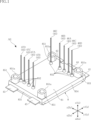
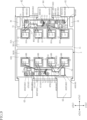
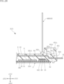
- FIG. 1 is a perspective view showing a semiconductor device according to a first embodiment of the present disclosure
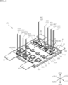
- FIG. FIG. 2 is a perspective view of main parts showing the semiconductor device according to the first embodiment of the present disclosure.
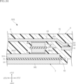
- FIG. 3 is a perspective view of main parts showing the semiconductor device according to the first embodiment of the present disclosure.
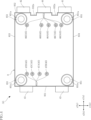
- FIG. 4 is a plan view showing the semiconductor device according to the first embodiment of the present disclosure;
- FIG. 5 is a fragmentary plan view showing the semiconductor device according to the first embodiment of the present disclosure;
- FIG. FIG. 6 is a main part side view showing the semiconductor device according to the first embodiment of the present disclosure.
- FIG. 7 is an enlarged plan view of main parts showing the semiconductor device according to the first embodiment of the present disclosure.
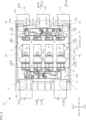
- FIG. 8 is a main part plan view showing the semiconductor device according to the first embodiment of the present disclosure.
- FIG. 9 is a fragmentary plan view showing the semiconductor device according to the first embodiment of the present disclosure.
- FIG. 10 is a side view showing the semiconductor device according to the first embodiment of the present disclosure;
- FIG. 11 is a bottom view showing the semiconductor device according to the first embodiment of the present disclosure;
- FIG. 12 is a cross-sectional view taken along line XII-XII in FIG.
- FIG. 13 is a cross-sectional view along line XIII-XIII in FIG.
- FIG. 14 is an enlarged cross-sectional view of main parts showing the semiconductor device according to the first embodiment of the present disclosure.
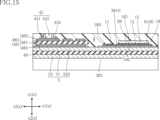
- FIG. 15 is an enlarged cross-sectional view of main parts showing the semiconductor device according to the first embodiment of the present disclosure.
- FIG. 16 is a cross-sectional view taken along line XVI--XVI of FIG.
- FIG. 17 is a cross-sectional view along line XVII-XVII of FIG.
- FIG. 18 is a cross-sectional view along line XVIII-XVIII in FIG. 19 is a cross-sectional view along line XIX-XIX in FIG. 5.
- FIG. FIG. 20 is a cross-sectional view along line XX-XX in FIG.
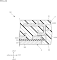
- FIG. 21 is an enlarged cross-sectional view of main parts showing the semiconductor device according to the first embodiment of the present disclosure.
- FIG. 22 is a perspective view showing a second conductive member of the semiconductor device according to the first embodiment of the present disclosure
- FIG. 23 is a perspective view showing a second conductive member of the semiconductor device according to the first embodiment of the present disclosure
- FIG. 24 is a plan view showing a second conductive member of the semiconductor device according to the first embodiment of the present disclosure
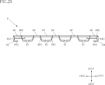
- FIG. 25 is a front view showing a second conductive member of the semiconductor device according to the first embodiment of the present disclosure
- FIG. 26 is a bottom view showing the second conductive member of the semiconductor device according to the first embodiment of the present disclosure
- FIG. 27 is a side view showing the second conductive member of the semiconductor device according to the first embodiment of the present disclosure
- FIG. 28 is an enlarged cross-sectional view of main parts showing a first modification of the semiconductor device according to the first embodiment of the present disclosure.
- FIG. 29 is an enlarged cross-sectional view of main parts showing a second modification of the semiconductor device according to the first embodiment of the present disclosure.
- FIG. 30 is an enlarged cross-sectional view of main parts showing a third modification of the semiconductor device according to the first embodiment of the present disclosure.
- FIG. 31 is an enlarged cross-sectional view of main parts showing a semiconductor device according to a second embodiment of the present disclosure.
- FIG. 32 is an enlarged cross-sectional view of main parts showing a first modification of the semiconductor device according to the second embodiment of the present disclosure.
- FIG. 33 is an enlarged cross-sectional view of main parts showing a semiconductor device according to a third embodiment of the present disclosure.
- FIG. 34 is an enlarged cross-sectional view of main parts showing a first modification of the semiconductor device according to the third embodiment of the present disclosure.
- FIG. 35 is an enlarged cross-sectional view of main parts showing a second modification of the semiconductor device according to the third embodiment of the present disclosure.
- FIG. 36 is an enlarged cross-sectional view of main parts showing a semiconductor device according to a fourth embodiment of the present disclosure.
- a certain entity A is formed on a certain entity B
- a certain entity A is formed on a certain entity B
- include a certain entity A is formed directly on a certain entity B” and "a certain entity A is formed on a certain entity B while another entity is interposed between the entity A and the entity B", unless otherwise specified.
- phrases “an entity A is placed on an entity B” and “an entity A is located on an entity B” include “an entity A is directly located on an entity B” and “an entity A is located on an entity B while another entity is interposed between the entity A and the entity B.”
- “an entity A is located on an entity B” includes “an entity A is adjacent to an entity B and an entity A is located on an entity B” and “an entity A is located on an entity B while another entity is interposed between an entity A and an entity B.”
- “an entity A overlaps an entity B in a certain direction” includes “an entity A that overlaps all of an entity B” and “an entity A that overlaps a part of an entity B”.
- the phrase “an object A is connected to an object B” includes objects A and B fixed in direct contact with each other, and objects A and B fixed to each other with one or more members interposed therebetween.
- First embodiment: 1 to 27 show a semiconductor device according to a first embodiment of the present disclosure.
- the semiconductor device A1 of this embodiment includes a plurality of first semiconductor elements 10A, a plurality of second semiconductor elements 10B, a support substrate 3, a first terminal 41, a second terminal 42, a plurality of third terminals 43, a fourth terminal 44, a plurality of control terminals 45, a control terminal support 48, a first conduction member 5, a second conduction member 6, and a sealing resin 8.
- FIG. 1 is a perspective view showing the semiconductor device A1.
- 2 and 3 are perspective views of essential parts showing the semiconductor device A1.
- FIG. 4 is a plan view showing the semiconductor device A1.
- FIG. 5 is a fragmentary plan view showing the semiconductor device A1.
- FIG. 6 is a main part side view showing the semiconductor device A1.
- FIG. 7 is an enlarged plan view of a main part showing the semiconductor device A1.
- 8 and 9 are plan views of essential parts showing the semiconductor device A1.
- FIG. 10 is a side view showing the semiconductor device A1.
- FIG. 11 is a bottom view showing the semiconductor device A1.
- FIG. 12 is a cross-sectional view taken along line XII-XII in FIG.
- FIG. 13 is a cross-sectional view along line XIII-XIII in FIG.
- FIG. 14 and 15 are enlarged cross-sectional views of essential parts showing the semiconductor device A1.
- FIG. 16 is a cross-sectional view taken along line XVI--XVI of FIG.
- FIG. 17 is a cross-sectional view along line XVII-XVII of FIG.
- FIG. 18 is a cross-sectional view along line XVIII-XVIII in FIG. 19 is a cross-sectional view along line XIX-XIX in FIG. 5.
- FIG. FIG. 20 is a cross-sectional view along line XX-XX in FIG.
- FIG. 21 is an enlarged cross-sectional view of a main portion showing the semiconductor device A1.
- FIG. 22 is a perspective view showing the second conductive member 6 of the semiconductor device A1.
- FIG. 22 is a perspective view showing the second conductive member 6 of the semiconductor device A1.
- FIG. 23 is a perspective view showing the second conductive member 6 of the semiconductor device A1.
- FIG. 24 is a plan view showing the second conductive member 6 of the semiconductor device A1.
- FIG. 25 is a front view showing the second conductive member 6 of the semiconductor device A1.
- FIG. 26 is a bottom view showing the second conductive member 6 of the semiconductor device A1.
- FIG. 27 is a side view showing the second conductive member 6 of the semiconductor device A1.
- the three mutually orthogonal directions are the x-direction, the y-direction, and the z-direction.
- the z direction is the thickness direction of the semiconductor device A1.
- the x direction is the horizontal direction in the plan view (see FIG. 4) of the semiconductor device A1.
- the y direction is the vertical direction in the plan view (see FIG. 4) of the semiconductor device A1.
- "planar view” means when viewed in the z direction.
- the x-direction is an example of the "first direction”
- the y-direction is an example of the "second direction”.
- Each of the plurality of first semiconductor elements 10A and the plurality of second semiconductor elements 10B is an electronic component that serves as the functional core of the semiconductor device A1.
- a constituent material of each first semiconductor element 10A and each second semiconductor element 10B is a semiconductor material mainly including SiC (silicon carbide), for example. This semiconductor material is not limited to SiC, and may be Si (silicon), GaN (gallium nitride), C (diamond), or the like.
- Each first semiconductor element 10A and each second semiconductor element 10B is, for example, a power semiconductor chip having a switching function such as a MOSFET (Metal Oxide Semiconductor Field Effect Transistor).
- MOSFET Metal Oxide Semiconductor Field Effect Transistor
- first semiconductor element 10A and the second semiconductor element 10B are MOSFETs
- other transistors such as an IGBT (Insulated Gate Bipolar Transistor) may be used.
- IGBT Insulated Gate Bipolar Transistor
- Each first semiconductor element 10A and each second semiconductor element 10B are the same element.
- Each first semiconductor element 10A and each second semiconductor element 10B is, for example, an n-channel MOSFET, but may be a p-channel MOSFET.
- the first semiconductor element 10A and the second semiconductor element 10B each have an element main surface 101 and an element rear surface 102, as shown in FIGS.
- the element main surface 101 and the element back surface 102 are separated in the z direction.
- the element main surface 101 faces the z1 direction
- the element back surface 102 faces the z2 direction.
- the semiconductor device A1 includes four first semiconductor elements 10A and four second semiconductor elements 10B, but the number of the first semiconductor elements 10A and the number of the second semiconductor elements 10B are not limited to this configuration, and can be changed as appropriate according to the performance required of the semiconductor device A1.
- four first semiconductor elements 10A and four second semiconductor elements 10B are arranged.
- the number of the first semiconductor elements 10A and the number of the second semiconductor elements 10B may be two or three, or may be five or more.
- the number of first semiconductor elements 10A and the number of second semiconductor elements 10B may be equal or different.
- the number of first semiconductor elements 10A and second semiconductor elements 10B is determined by the current capacity handled by semiconductor device A1.
- the semiconductor device A1 is configured, for example, as a half-bridge switching circuit.
- the plurality of first semiconductor elements 10A form an upper arm circuit of the semiconductor device A1
- the plurality of second semiconductor elements 10B form a lower arm circuit.
- the plurality of first semiconductor elements 10A are connected in parallel
- the plurality of second semiconductor elements 10B are connected in parallel.
- Each first semiconductor element 10A and each second semiconductor element 10B are connected in series to form a bridge layer.
- each of the plurality of first semiconductor elements 10A is mounted on a first conductive portion 32A of the support substrate 3, which will be described later.
- the plurality of first semiconductor elements 10A are arranged, for example, in the y direction and separated from each other.
- Each first semiconductor element 10A is electrically connected to the first conductive portion 32A via the conductive bonding material 19 .
- the element rear surface 102 faces the first conductive portion 32A.
- the plurality of first semiconductor elements 10A may be mounted on a metal member different from a part of the DBC substrate or the like.
- the metal member is an example of the "first conductive portion". This metal member may be supported, for example, by the first conductive portion 32A.
- each of the plurality of second semiconductor elements 10B is mounted on a second conductive portion 32B of the support substrate 3 which will be described later.
- the plurality of second semiconductor elements 10B are arranged, for example, in the y direction and separated from each other.
- Each second semiconductor element 10B is electrically connected to the second conductive portion 32B via the conductive bonding material 19 .
- the element rear surface 102 faces the second conductive portion 32B.
- the plurality of first semiconductor elements 10A and the plurality of second semiconductor elements 10B overlap when viewed in the x direction, but they do not have to overlap.
- the plurality of second semiconductor elements 10B may be mounted on a metal member different from a portion of the DBC substrate or the like.
- the metal member is an example of the "second conductive part”. This metal member may be supported, for example, by the second conductive portion 32B.
- the plurality of first semiconductor elements 10A and the plurality of second semiconductor elements 10B each have a first principal surface electrode 11, a second principal surface electrode 12, a third principal surface electrode 13 and a back surface electrode 15.
- the configurations of the first main surface electrode 11, the second main surface electrode 12, the third main surface electrode 13, and the rear surface electrode 15 described below are common to each first semiconductor element 10A and each second semiconductor element 10B.
- the first principal surface electrode 11 , the second principal surface electrode 12 and the third principal surface electrode 13 are provided on the element principal surface 101 .
- the first principal surface electrode 11, the second principal surface electrode 12 and the third principal surface electrode 13 are insulated by an insulating film (not shown).
- the back surface electrode 15 is provided on the element back surface 102 .
- the first main surface electrode 11 is, for example, a gate electrode, and receives a drive signal (for example, gate voltage) for driving the first semiconductor element 10A (second semiconductor element 10B).
- the second main surface electrode 12 is, for example, a source electrode through which a source current flows.
- the third principal-surface electrode 13 is, for example, a source sense electrode through which a source current flows.
- Back surface electrode 15 is, for example, a drain electrode through which drain current flows.
- the back surface electrode 15 covers the entire area (or substantially the entire area) of the element back surface 102 .
- the back surface electrode 15 is configured by Ag (silver) plating, for example.
- each first semiconductor element 10A switches between a conductive state and a cutoff state in accordance with the drive signal.
- a current flows from the back surface electrode 15 (drain electrode) to the second main surface electrode 12 (source electrode) in the conductive state, and does not flow in the cutoff state. That is, each first semiconductor element 10A (each second semiconductor element 10B) performs a switching operation.
- the semiconductor device A1 uses the switching functions of the plurality of first semiconductor elements 10A and the plurality of second semiconductor elements 10B to convert, for example, a DC voltage input between one fourth terminal 44 and two first and second terminals 41 and 42 into an AC voltage and output the AC voltage from a third terminal 43.
- the semiconductor device A1 includes a thermistor 17 as shown in FIGS. 5, 8, 9, and the like.
- the thermistor 17 is used as a temperature detection sensor.
- a temperature-sensitive diode or the like may be provided, or the thermistor 17 or the like may not be provided.
- the support substrate 3 supports the plurality of first semiconductor elements 10A and the plurality of second semiconductor elements 10B.
- the specific configuration of the support substrate 3 is not limited at all, and is composed of, for example, a DBC (Direct Bonded Copper) substrate or an AMB (Active Metal Brazing) substrate.
- the support substrate 3 includes an insulating layer 31 , a first conductive portion 32A, a second conductive portion 32B and a back metal layer 33 .
- the support substrate 3 of the present embodiment further includes a first metal portion 35 and a second metal portion 36 .
- the dimension of the support substrate 3 in the z direction is, for example, 0.4 mm or more and 3.0 mm or less.
- the insulating layer 31 is, for example, ceramics with excellent thermal conductivity. Such ceramics include, for example, SiN (silicon nitride).
- the insulating layer 31 is not limited to ceramics, and may be an insulating resin sheet or the like.
- the insulating layer 31 has, for example, a rectangular shape in plan view.
- the z-direction dimension of the insulating layer 31 is, for example, 0.05 mm or more and 1.0 mm or less.
- the first conductive portion 32A supports the plurality of first semiconductor elements 10A
- the second conductive portion 32B supports the plurality of second semiconductor elements 10B.
- the first conductive portion 32A and the second conductive portion 32B are formed on the upper surface of the insulating layer 31 (the surface facing the z1 direction).
- a constituent material of the first conductive portion 32A and the second conductive portion 32B includes, for example, Cu (copper).
- the constituent material may contain Al (aluminum) instead of Cu.
- the first conductive portion 32A and the second conductive portion 32B are separated in the x direction.
- the first conductive portion 32A is located on the x1 direction side of the second conductive portion 32B.
- Each of the first conductive portion 32A and the second conductive portion 32B has, for example, a rectangular shape in plan view.
- the first conductive portion 32A and the second conductive portion 32B, together with the first conductive member 5 and the second conductive member 6, configure the path of the main circuit current switched by the plurality of first semiconductor elements 10A and the plurality of second semiconductor elements 10B.
- the first conductive portion 32A has a first main surface 301A.
- the first main surface 301A is a plane facing the z1 direction.
- a plurality of first semiconductor elements 10A are bonded to the first main surface 301A of the first conductive portion 32A via conductive bonding materials 19, respectively.
- the second conductive portion 32B has a second main surface 301B.
- the second main surface 301B is a plane facing the z1 direction.
- a plurality of second semiconductor elements 10B are bonded to the second main surface 301B of the second conductive portion 32B via the conductive bonding material 19 .
- a constituent material of the conductive bonding material 19 is not particularly limited, and may be, for example, solder, a metal paste material, or a sintered metal.
- the z-direction dimension of the first conductive portion 32A and the second conductive portion 32B is, for example, 0.1 mm or more and 1.5 mm or less.
- the first metal portion 35 is formed on the insulating layer 31 in the same manner as the first conductive portion 32A and the second conductive portion 32B.
- the first metal portion 35 is separated from the first conductive portion 32A and the second conductive portion 32B, and is insulated from the first conductive portion 32A and the second conductive portion 32B.
- the first metal part 35 is made of metal.
- Examples of the material of the first metal portion 35 include the same material as the first conductive portion 32A and the second conductive portion 32B.
- the size of the first metal portion 35 in the z direction is not limited at all, and is, for example, the same as that of the first conductive portion 32A and the second conductive portion 32B.
- the arrangement of the first metal part 35 is not limited at all, and in the present embodiment, as shown in FIG.
- the first conductive portion 32A has a recess shaped to accommodate the first metal portion 35 when viewed in the z direction.
- the shape of the first metal portion 35 is not limited at all, and in the illustrated example, it is a rectangular shape with the x direction as the longitudinal direction.
- the second metal part 36 is made of metal.
- Examples of the material of the second metal portion 36 include the same material as the first conductive portion 32A and the second conductive portion 32B.
- the size of the second metal portion 36 in the z direction is not limited at all, and is, for example, the same as that of the first conductive portion 32A and the second conductive portion 32B.
- the arrangement of the second metal part 36 is not limited at all, and in the present embodiment, as shown in FIG.
- the first conductive portion 32A has a recess shaped to accommodate the second metal portion 36 when viewed in the z-direction.
- the shape of the second metal portion 36 is not limited at all, and in the illustrated example, it is a rectangular shape with the x direction as the longitudinal direction.
- the first metal portion 35 and the second metal portion 36 are spaced apart in the y direction with a portion of the first conductive portion 32A interposed therebetween.
- the back metal layer 33 is formed on the lower surface of the insulating layer 31 (the surface facing the z2 direction).
- the constituent material of the back metal layer 33 is the same as the constituent material of the first metal layer 32 .
- the back metal layer 33 has a back surface 302 .
- the back surface 302 is a plane facing the z2 direction.
- the rear surface 302 is exposed from the sealing resin 8, for example, in the example shown in FIG.
- a heat dissipating member for example, a heat sink
- the rear surface 302 may be covered with the sealing resin 8 without being exposed from the sealing resin 8 .
- the back metal layer 33 overlaps both the first conductive portion 32A and the second conductive portion 32B in plan view. Further, the back metal layer 33 overlaps both the first metal portion 35 and the second metal portion 36 in plan view.
- the first terminal 41, the second terminal 42, the plurality of third terminals 43, and the fourth terminal 44 are each made of a plate-like metal plate.
- the constituent material of this metal plate is, for example, Cu or a Cu alloy.
- the semiconductor device A1 has one first terminal 41, one second terminal 42, one fourth terminal 44, and two third terminals 43.
- the number of each terminal is not limited at all.
- a DC voltage to be converted into power is input to the first terminal 41, the second terminal 42 and the fourth terminal 44.
- the fourth terminal 44 is a positive electrode (P terminal), and the first terminal 41 and the second terminal 42 are each a negative electrode (N terminal).
- P terminal positive electrode
- N terminal negative electrode
- Each of the first terminal 41 , the second terminal 42 , the plurality of third terminals 43 , and the fourth terminal 44 includes a portion covered with the sealing resin 8 and a portion exposed from the sealing resin 8 .
- the fourth terminal 44 is conductively joined to the first conductive portion 32A, as shown in FIG.
- the method of conductive bonding is not limited at all, and methods such as ultrasonic bonding, laser bonding, welding, or methods using solder, metal paste, silver sintered bodies, etc., are appropriately adopted.
- the fourth terminal 44 is positioned on the x1 direction side with respect to the plurality of first semiconductor elements 10A and the first conductive portions 32A.
- the fourth terminal 44 is electrically connected to the first conductive portion 32A, and is electrically connected to the back electrode 15 (drain electrode) of each first semiconductor element 10A via the first conductive portion 32A.
- the first terminal 41 and the second terminal 42 are separated from the first conductive portion 32A, as shown in FIG.
- the first terminal 41 and the second terminal 42 are joined to the second conductive member 6, respectively, as shown in FIGS.
- the first terminal 41 and the second terminal 42 may be configured to be electrically connected to the second conduction member 6, and for example, may be configured to be integrally formed with the second conduction member 6 without having a joint portion or the like.
- the first terminals 41 and the second terminals 42 are positioned on the x1 direction side with respect to the plurality of first semiconductor elements 10A and the first conductive portions 32A, respectively, as shown in FIGS.
- the first terminal 41 and the second terminal 42 are each electrically connected to the second conductive member 6 and electrically connected to the second main surface electrode 12 (source electrode) of each second semiconductor element 10B via the second conductive member 6 .
- the first terminal 41, the second terminal 42 and the fourth terminal 44 each protrude from the sealing resin 8 in the x1 direction in the semiconductor device A1.
- the first terminal 41, the second terminal 42 and the fourth terminal 44 are separated from each other.
- the first terminal 41 and the second terminal 42 are positioned opposite to each other with the fourth terminal 44 interposed therebetween in the y direction.
- the first terminal 41 is positioned on the y1 direction side of the fourth terminal 44
- the second terminal 42 is positioned on the y2 direction side of the fourth terminal 44 .
- the first terminal 41, the second terminal 42 and the fourth terminal 44 overlap each other when viewed in the y direction.
- Each of the two third terminals 43 is conductively joined to the second conductive portion 32B as can be understood from FIGS. 8, 9 and 12 .
- the method of conductive bonding is not limited at all, and methods such as ultrasonic bonding, laser bonding, welding, or methods using solder, metal paste, silver sintered bodies, etc., are appropriately employed.
- Each of the two third terminals 43 is positioned on the x2 direction side with respect to the plurality of second semiconductor elements 10B and the second conductive portions 32B, as shown in FIG. 8 and the like.
- Each third terminal 43 is electrically connected to the second conductive portion 32B, and is electrically connected to the back surface electrode 15 (drain electrode) of each second semiconductor element 10B via the second conductive portion 32B.
- the number of third terminals 43 is not limited to two, and may be, for example, one or three or more. For example, if there is one third terminal 43, it is desirable that it is connected to the central portion of the second conductive portion 32B in the y direction.
- the plurality of control terminals 45 are pin-shaped terminals for controlling each first semiconductor element 10A and each second semiconductor element 10B.
- the plurality of control terminals 45 includes a plurality of first control terminals 46A-46E and a plurality of second control terminals 47A-47D.
- a plurality of first control terminals 46A to 46E are used for control of each first semiconductor element 10A.
- a plurality of second control terminals 47A to 47D are used for control of each second semiconductor element 10B.
- a plurality of first control terminals 46A to 46E are arranged at intervals in the y direction. As shown in FIGS. 8, 13 and 20, each of the first control terminals 46A to 46E is supported by the first conductive portion 32A via a control terminal support 48 (first support portion 48A to be described later). Each of the first control terminals 46A-46E is located between the plurality of first semiconductor elements 10A and the first terminal 41, the second terminal 42 and the fourth terminal 44 in the x-direction, as shown in FIGS.
- the first control terminal 46A is a terminal (gate terminal) for driving signal input of the plurality of first semiconductor elements 10A.
- a drive signal for driving the plurality of first semiconductor elements 10A is input to the first control terminal 46A (for example, a gate voltage is applied).
- the first control terminal 46B is a terminal (source sense terminal) for detecting source signals of the plurality of first semiconductor elements 10A.
- a voltage (voltage corresponding to the source current) applied to each second main surface electrode 12 (source electrode) of the plurality of first semiconductor elements 10A is detected from the first control terminal 46B.
- the first control terminal 46C and the first control terminal 46D are terminals that are electrically connected to the thermistor 17.
- the first control terminal 46E is a terminal for drain signal detection (drain sense terminal) of the plurality of first semiconductor elements 10A.
- a voltage (a voltage corresponding to the drain current) applied to each back surface electrode 15 (drain electrode) of the plurality of first semiconductor elements 10A is detected from the first control terminal 46E.
- a plurality of second control terminals 47A to 47D are arranged at intervals in the y direction. As shown in FIGS. 8 and 13, each of the second control terminals 47A to 47D is supported by the second conductive portion 32B via a control terminal support 48 (second support portion 48B to be described later). Each of the second control terminals 47A-47D is positioned between the plurality of second semiconductor elements 10B and the two third terminals 43 in the x-direction, as shown in FIGS.
- the second control terminal 47A is a terminal (gate terminal) for driving signal input of the plurality of second semiconductor elements 10B.
- a drive signal for driving the plurality of second semiconductor elements 10B is input to the second control terminal 47A (for example, a gate voltage is applied).
- the second control terminal 47B is a terminal (source sense terminal) for source signal detection of the plurality of second semiconductor elements 10B.
- a voltage (voltage corresponding to the source current) applied to each second main surface electrode 12 (source electrode) of the plurality of second semiconductor elements 10B is detected from the second control terminal 47B.
- the second control terminal 47C and the second control terminal 47D are terminals electrically connected to the thermistor 17 .
- the plurality of control terminals 45 each include a holder 451 and a metal pin 452.
- the holder 451 is made of a conductive material. As shown in FIGS. 14 and 15, the holder 451 is bonded to the control terminal support 48 (first metal layer 482 described later) via a conductive bonding material 459 .
- the holder 451 includes a tubular portion, an upper flange, and a lower flange. The upper brim part is connected to the upper part of the tubular part, and the lower end brim part is connected to the lower part of the tubular part.
- a metal pin 452 is inserted through at least the upper end collar portion and the cylindrical portion of the holder 451 .
- the holder 451 is covered with the sealing resin 8 (second projecting portion 852 described later).
- the metal pin 452 is a rod-shaped member extending in the z-direction.
- the metal pin 452 is supported by being press-fitted into the holder 451 .
- the metal pin 452 is electrically connected to the control terminal support 48 (first metal layer 482 described later) through at least the holder 451 . 14 and 15 , when the lower end of the metal pin 452 (the end in the z2 direction) is in contact with the conductive bonding material 459 in the insertion hole of the holder 451, the metal pin 452 is electrically connected to the control terminal support 48 via the conductive bonding material 459.
- the control terminal support 48 supports multiple control terminals 45 .
- Control terminal support 48 is interposed between first major surface 301A and second major surface 301B and plurality of control terminals 45 in the z-direction.
- the control terminal support 48 includes a first support 48A and a second support 48B.
- the first support portion 48A is arranged on the first conductive portion 32A and supports the plurality of first control terminals 46A to 46E among the plurality of control terminals 45A.
- the first support portion 48A is joined to the first conductive portion 32A via a joining material 49, as shown in FIG.
- the bonding material 49 may be conductive or insulating, and solder is used, for example.
- the second support portion 48B is arranged on the second conductive portion 32B and supports the plurality of second control terminals 47A to 47D among the plurality of control terminals 45. As shown in FIG.
- the second support portion 48B is joined to the second conductive portion 32B via a joining material 49, as shown in FIG.
- the control terminal support 48 (each of the first support 48A and the second support 48B) is composed of, for example, a DBC (Direct Bonded Copper) substrate.
- the control terminal support 48 has an insulating layer 481, a first metal layer 482 and a second metal layer 483 laminated together.
- the insulating layer 481 is made of ceramics, for example.
- the insulating layer 481 has, for example, a rectangular shape in plan view.
- the first metal layer 482 is formed on the upper surface of the insulating layer 481, as shown in FIGS. Each control terminal 45 is erected on the first metal layer 482 .
- the first metal layer 482 is Cu or Cu alloy, for example.
- the first metal layer 482 includes a first portion 482A, a second portion 482B, a third portion 482C, a fourth portion 482D, a fifth portion 482E and a sixth portion 482F.
- the first portion 482A, the second portion 482B, the third portion 482C, the fourth portion 482D, the fifth portion 482E and the sixth portion 482F are separated from each other and insulated.
- a plurality of wires 71 are joined to the first portion 482A, and the wires 71 are electrically connected to the first main surface electrodes 11 (gate electrodes) of the first semiconductor elements 10A (second semiconductor elements 10B).
- a plurality of wires 73 are connected to the first portion 482A and the sixth portion 482F.
- the sixth portion 482F is electrically connected to the first main surface electrode 11 (gate electrode) of each first semiconductor element 10A (each second semiconductor element 10B) through the wire 73 and the wire 71.
- the first control terminal 46A is joined to the sixth portion 482F of the first support portion 48A
- the second control terminal 47A is joined to the sixth portion 482F of the second support portion 48B.
- a plurality of wires 72 are joined to the second portion 482B, and the wires 72 are electrically connected to the second principal surface electrodes 12 (source electrodes) of the first semiconductor elements 10A (second semiconductor elements 10B).
- the first control terminal 46B is joined to the second portion 482B of the first support portion 48A
- the second control terminal 47B is joined to the second portion 482B of the second support portion 48B.
- the thermistor 17 is joined to the third portion 482C and the fourth portion 482D. As shown in FIG. 8, the first control terminals 46C and 46D are joined to the third portion 482C and the fourth portion 482D of the first support portion 48A, and the second control terminals 47C and 47D are joined to the third portion 482C and the fourth portion 482D of the second support portion 48B.
- the wire 74 is joined to the fifth portion 482E of the first support portion 48A, and is electrically connected to the first conductive portion 32A via the wire 74. As shown in FIG. 8, the first control terminal 46E is joined to the fifth portion 482E of the first support portion 48A. The fifth portion 482E of the second support portion 48B is not electrically connected to other components.
- Each of the wires 71 to 74 described above is, for example, a bonding wire.
- the constituent material of each wire 71-74 includes, for example, Au (gold), Al or Cu.
- the second metal layer 483 is formed on the lower surface of the insulating layer 481, as shown in FIGS.
- the second metal layer 483 of the first support portion 48A is joined to the first conductive portion 32A via the joining material 49, as shown in FIG.
- the second metal layer 483 of the second support portion 48B is bonded to the second conductive portion 32B via the bonding material 49, as shown in FIG.
- the first conductive member 5 and the second conductive member 6 are separated from the first main surface 301A and the second main surface 301B in the z1 direction, and overlap the first main surface 301A and the second main surface 301B in plan view.
- the first conduction member 5 and the second conduction member 6 are each made of a metal plate material.
- the metal is for example Cu or a Cu alloy.
- the first conductive member 5 and the second conductive member 6 are suitably bent metal plate members.
- the first conductive member 5 is connected to the second main surface electrode 12 (source electrode) and the second conductive portion 32B of each first semiconductor element 10A, and conducts the second main surface electrode 12 and the second conductive portion 32B of each first semiconductor element 10A.
- the first conductive member 5 constitutes a path of main circuit current switched by the plurality of first semiconductor elements 10A.
- the first conducting member 5 includes a main portion 51, a plurality of first joint portions 52 and a plurality of second joint portions 53, as shown in FIGS.
- the main portion 51 is a strip-shaped portion located between the plurality of first semiconductor elements 10A and the second conductive portions 32B in the x direction and extending in the y direction in plan view.
- the main portion 51 overlaps both the first conductive portion 32A and the second conductive portion 32B in plan view, is separated from the first main surface 301A and the second main surface 301B in the z direction in the z direction, and is separated from the first main surface 301A and the second main surface 301B in the z1 direction in the plan view. As shown in FIG.
- the main portion 51 is positioned in the z2 direction with respect to a third path portion 66 and a fourth path portion 67 of the second conduction member 6, which will be described later, and is closer to the first main surface 301A and the second main surface 301B than the third path portion 66 and the fourth path portion 67.
- the main portion 51 is arranged parallel to the first main surface 301A and the second main surface 301B, and overlaps both the first conductive portion 32A and the second conductive portion 32B in plan view.
- the main portion 51 extends continuously in the y-direction corresponding to the region where the plurality of first semiconductor elements 10A are arranged.
- a plurality of first openings 514 are formed in the main portion 51, as shown in FIGS. 7, 8, 13, and the like.
- Each of the plurality of first openings 514 is a through hole penetrating in, for example, the z-direction (thickness direction of the main portion 51).
- the plurality of first openings 514 are arranged at intervals in the y1 direction.
- the plurality of first openings 514 are provided corresponding to each of the plurality of first semiconductor elements 10A.
- the main portion 51 is provided with four first openings 514, and the first openings 514 and the plurality (four) of the first semiconductor elements 10A are at the same position in the y direction.
- each first opening 514 overlaps the gap between the first conductive portion 32A and the second conductive portion 32B in plan view.
- the plurality of first openings 514 are formed to facilitate the flow of the resin material between the upper side (z1 direction side) and the lower side (z2 direction side) in the vicinity of the main portion 51 (first conductive member 5) when injecting a fluid resin material to form the sealing resin 8.
- each first joint portion 52 and the plurality of second joint portions 53 are each connected to the main portion 51 via bent portions and arranged corresponding to the plurality of first semiconductor elements 10A.
- each first joint portion 52 is positioned in the x1 direction with respect to the main portion 51 .
- Each second joint portion 53 is positioned in the x2 direction with respect to the main portion 51 .
- each first joint portion 52 and the corresponding second main surface electrode 12 of any one of the first semiconductor elements 10A are joined via a conductive joint material 59 .
- Each second joint portion 53 and the second conductive portion 32B are joined via a conductive joint material 59 .
- a constituent material of the conductive bonding material 59 is not particularly limited, and may be, for example, solder, a metal paste material, or a sintered metal.
- the second conductive member 6 is connected to the second main surface electrode 12 (source electrode) of each second semiconductor element 10B and the first terminal 41 and the second terminal 42, and conducts the second main surface electrode 12 of each second semiconductor element 10B to the first terminal 41 and the second terminal 42.
- the second conductive member 6 constitutes a path of main circuit current switched by the plurality of second semiconductor elements 10B. 7 and FIGS. 21 to 27, the second conducting member 6 includes a plurality of third joints 61, a fourth joint 62, a fifth joint 63, a first path part 64, a second path part 65, a plurality of third path parts 66 and a fourth path part 67.
- the plurality of third bonding portions 61 are portions that are individually bonded to the plurality of second semiconductor elements 10B. Each third bonding portion 61 and the second principal surface electrode 12 of each second semiconductor element 10B are bonded via a conductive bonding material 69 .
- a constituent material of the conductive bonding material 69 is not particularly limited, and may be, for example, solder, a metal paste material, or a sintered metal.
- two third joint portions 61 are joined to the second principal surface electrode 12 of one second semiconductor element 10B. These two third joint portions 61 are separated in the y direction with the central portion of the second principal surface electrode 12 interposed therebetween.
- the fourth joint portion 62 is a portion that is joined to the first terminal 41 .
- the fourth joint portion 62 and the first terminal 41 are joined via a conductive joint material 69 .
- a constituent material of the conductive bonding material 69 is not particularly limited, and may be, for example, solder, a metal paste material, or a sintered metal.
- the fifth joint portion 63 is a portion that is joined to the second terminal 42 .
- the fourth joint portion 62 and the second terminal 42 are joined via a conductive joint material 69 .
- a constituent material of the conductive bonding material 69 is not particularly limited, and may be, for example, solder, a metal paste material, or a sintered metal.
- the first path portion 64 is interposed between the multiple third joint portions 61 and the fourth joint portions 62 .
- the first path portion 64 is connected to the fourth joint portion 62 via a bent portion.
- the first path portion 64 overlaps the first conductive portion 32A and the first metal portion 35 in plan view.
- the first path portion 64 has a shape extending in the x direction as a whole.
- the first path portion 64 includes a first belt-shaped portion 641 , a first connecting portion 642 and a first connecting portion 643 .
- the first band-shaped portion 641 is positioned in the z1 direction with respect to the fourth joint portion 62 and substantially parallel to the first major surface 301A.
- the first band-shaped portion 641 has a shape extending in the x direction as a whole.
- the first strip 641 has a recess 649 .
- the recessed portion 649 is a part of the first band-shaped portion 641 recessed in the y1 direction. In FIG. 5 , the first metal portion 35 appears through the recess 649 .
- the first connecting portion 642 is a portion located in the z2 direction with respect to the first band-shaped portion 641 .
- the shape and size of the first connection portion 642 are not limited at all, and in the illustrated example, it is a rectangular shape with the x direction as the longitudinal direction.
- the first connection portion 642 is connected to the first metal portion 35.
- the first path portion 64 is connected to the support substrate 3 .
- the first connecting portion 642 is bonded to the first metal portion 35 via the conductive bonding material 69 .
- the first connecting portion 642 may be joined to the first metal portion 35 by a method such as ultrasonic joining, laser joining, or welding. Also, in the illustrated example, the first connection portion 642 protrudes from the first metal portion 35 in the y1 direction.
- the first connecting portion 643 connects the end of the first band-shaped portion 641 in the y1 direction and the end of the first connecting portion 642 in the y1 direction.
- the first connecting portion 643 is shaped along the z-direction and has a long rectangular shape with the x-direction as the longitudinal direction.
- the second path portion 65 is interposed between the multiple third joint portions 61 and the fifth joint portions 63 .
- the second path portion 65 is connected to the fifth joint portion 63 via a bent portion.
- the second path portion 65 overlaps the first conductive portion 32A and the second metal portion 36 in plan view.
- the second path portion 65 has a shape extending in the x direction as a whole.
- the second path portion 65 includes a second strip portion 651 , a second connection portion 652 and a second connection portion 653 .
- the second band-shaped portion 651 is positioned in the z1 direction with respect to the fifth joint portion 63 and substantially parallel to the first main surface 301A.
- the second band-shaped portion 651 has a shape extending in the x direction as a whole.
- the second strip 651 has a recess 659 .
- the recessed portion 659 is a part of the second band-shaped portion 651 recessed in the y2 direction. In FIG. 5, the second metal portion 36 appears through the recess 659.
- the second connecting portion 652 is a portion located in the z2 direction with respect to the second band-shaped portion 651 .
- the shape and size of the second connection portion 652 are not limited at all, and in the illustrated example, it has a long rectangular shape with the x direction as the longitudinal direction.
- the second connection portion 652 is connected to the second metal portion 36 .
- the second path portion 65 is connected to the support substrate 3 .
- the second connection portion 652 is bonded to the second metal portion 36 via the conductive bonding material 69 .
- the second connecting portion 652 may be joined to the second metal portion 36 by ultrasonic joining, laser joining, welding, or other techniques. Also, in the illustrated example, the second connection portion 652 protrudes from the second metal portion 36 in the y2 direction.
- the second connecting portion 653 connects the y2 direction side end of the second strip portion 651 and the y2 direction side end of the second connecting portion 652 .
- the second connecting portion 653 is shaped along the z-direction and has a long rectangular shape with the x-direction as the longitudinal direction.
- the configuration of the first path portion 64 is linearly symmetrical about the center line extending in the x direction, for example, and can be appropriately adopted for the second path portion 65 as well.
- the plurality of third path portions 66 are individually connected to the plurality of third joint portions 61 .
- Each third path portion 66 has a shape extending in the x direction and is arranged apart from each other in the y direction.
- the number of the plurality of third path portions 66 is not limited at all, and five third path portions 66 are arranged in the illustrated example.
- Each third path portion 66 is arranged so as to be positioned between the plurality of third joint portions 61 in the y direction or positioned outside the plurality of third joint portions 61 in the y direction.
- the third path portion 66 is positioned in the z1 direction with respect to the third joint portion 61 .
- the third path portion 66 and the third joint portion 61 are connected via a bent portion.
- Concave portions 669 are formed in the two third path portions 66 positioned on both outer sides in the y direction.
- the recess 669 is recessed from the inside toward the outside in the y direction.
- two recesses 669 are formed in each third path portion 66 .
- the first conductive portion 32A and the second conductive portion 32B appear through these recesses 669. As shown in FIG.
- the fourth path portion 67 is connected to the ends of the plurality of third path portions 66 in the x1 direction.
- the fourth path portion 67 has a shape elongated in the y direction.
- the fourth path portion 67 is connected to the ends of the first strip portion 641 of the first path portion 64 and the second strip portion 651 of the second path portion 65 in the x2 direction.
- the first path portion 64 is connected to the y1 direction side end of the fourth path portion 67 .
- the second path portion 65 is connected to the y2 direction side end of the fourth path portion 67 .
- the sealing resin 8 covers the plurality of first semiconductor elements 10A, the plurality of second semiconductor elements 10B, the support substrate 3 (excluding the back surface 302), the first terminals 41, the second terminals 42, the plurality of third terminals 43, and the fourth terminals 44, the plurality of control terminals 45, the control terminal support 48, the first conductive member 5, the second conductive member 6, and the wires 71 to 74, respectively.
- Sealing resin 8 is made of, for example, black epoxy resin.
- the sealing resin 8 is formed by molding, for example.
- the sealing resin 8 has, for example, an x-direction dimension of about 35 mm to 60 mm, a y-direction dimension of about 35 mm to 50 mm, and a z-direction dimension of about 4 mm to 15 mm. These dimensions are the largest part sizes along each direction.
- the sealing resin 8 has a resin main surface 81, a resin back surface 82 and a plurality of resin side surfaces 831-834.
- the resin main surface 81 and the resin back surface 82 are separated in the z-direction as shown in FIGS.
- the resin main surface 81 faces the z1 direction
- the resin back surface 82 faces the z2 direction.
- a plurality of control terminals 45 protrude from the resin main surface 81 .
- the resin back surface 82 has a frame shape surrounding the back surface 302 of the support substrate 3 (the lower surface of the back surface metal layer 33) in plan view.
- the back surface 302 of the support substrate 3 is exposed from the resin back surface 82 and is flush with the resin back surface 82, for example.
- Each of the plurality of resin side surfaces 831 to 834 is connected to both the resin main surface 81 and the resin back surface 82 and sandwiched between them in the z direction.
- the resin side surface 831 and the resin side surface 832 are separated in the x direction.
- the resin side surface 831 faces the x2 direction, and the resin side surface 832 faces the x1 direction.
- Two third terminals 43 protrude from the resin side surface 831
- the first terminal 41 , the second terminal 42 and the fourth terminal 44 protrude from the resin side surface 832 .
- the resin side surface 833 and the resin side surface 834 are separated in the y direction.
- the resin side surface 833 faces the y2 direction
- the resin side surface 834 faces the y1 direction.
- the resin side surface 832 is formed with a plurality of recesses 832a.
- Each recess 832a is a portion recessed in the x direction in plan view.
- the plurality of recesses 832a include those formed between the first terminal 41 and the fourth terminal 44 and those formed between the second terminal 42 and the fourth terminal 44 in plan view.
- the plurality of recesses 832a are provided to increase the creeping distance along the resin side surface 832 between the first terminal 41 and the fourth terminal 44 and the creeping distance along the resin side surface 832 between the second terminal 42 and the fourth terminal 44.
- the sealing resin 8 has a plurality of first projecting portions 851, a plurality of second projecting portions 852, and resin voids 86, as shown in FIGS.
- Each of the plurality of first protrusions 851 protrudes from the resin main surface 81 in the z direction.
- the plurality of first protrusions 851 are arranged near the four corners of the sealing resin 8 in plan view.
- a first protruding end face 851a is formed at the tip of each first protruding portion 851 (the end in the z1 direction).
- Each first projecting end surface 851a of the plurality of first projecting portions 851 is parallel (or substantially parallel) to the resin main surface 81 and on the same plane (xy plane).
- Each first projecting portion 851 has, for example, a bottomed hollow truncated cone shape.
- the plurality of first protrusions 851 are used as spacers when the semiconductor device A1 is mounted on a control circuit board or the like of the device that uses the power source generated by the semiconductor device A1.
- Each of the plurality of first protrusions 851 has a recess 851b and an inner wall surface 851c formed in the recess 851b.
- the shape of each first projecting portion 851 may be columnar, and is preferably columnar. It is preferable that the concave portion 851b has a columnar shape, and the inner wall surface 851c has a single perfect circle shape in a plan view.
- the semiconductor device A1 may be mechanically fixed to a control circuit board or the like by a method such as screwing.
- the inner wall surfaces 851c of the recesses 851b of the plurality of first projections 851 can be formed with internal threads.
- An insert nut may be embedded in the concave portion 851 b of the plurality of first protrusions 851 .
- the plurality of second protrusions 852 protrude from the resin main surface 81 in the z-direction, as shown in FIG. 13 and the like.
- the plurality of second projecting portions 852 overlap the plurality of control terminals 45 in plan view.
- Each metal pin 452 of the plurality of control terminals 45 protrudes from each second protrusion 852 .
- Each second protrusion 852 has a truncated cone shape.
- the second protrusion 852 covers the holder 451 and part of the metal pin 452 at each control terminal 45 .
- the second conduction member 6 is connected to the support substrate 3.
- the second conduction member 6 electrically connects the plurality of second semiconductor elements 10B and the first terminals 41 .
- the first terminal 41 is positioned on the x1 direction side opposite to the plurality of second semiconductor elements 10B across the first conductive portion 32A. Therefore, it is assumed that heat is generated when a large current flows through the second conductive member 6 . Since the second conductive member 6 is connected to the support substrate 3, the heat generated in the second conductive member 6 can be transferred to the support substrate 3 and radiated to the outside of the semiconductor device A1. Therefore, according to the semiconductor device A1, it is possible to increase the current and promote heat dissipation.
- the second conducting member 6 has a first path portion 64 . At least about half of the main circuit current of the plurality of second semiconductor elements 10B flows through the first path portion 64 . By connecting such a first path portion 64 to the support substrate 3, the heat generated by the energization can be released to the support substrate 3 more efficiently.
- the second conduction member 6 has a second path portion 65, and the second path portion 65 is connected to the support substrate 3 (second metal portion 36). This allows heat to escape from both the first path portion 64 and the second path portion 65 to the support substrate 3 . Therefore, the heat dissipation efficiency of the semiconductor device A1 can be further improved.
- first path portion 64 connected to the first terminal 41 and the second path portion 65 connected to the second terminal 42 are connected to the support substrate 3, heat generated from external devices and devices connected to the semiconductor device A1 can be released to the support substrate 3. Thereby, heat from the outside can be suppressed from reaching, for example, the plurality of second semiconductor elements 10B.
- a first connection portion 642 of the first path portion 64 is connected to the first metal portion 35 of the support substrate 3 .
- the first metal portion 35 is insulated from the first conductive portion 32A and the second conductive portion 32B. Thereby, even if the first path portion 64 is conductively joined to the first metal portion 35, it is possible to avoid forming an unintended current path.
- Conductive joining is generally a joining method with high heat transfer efficiency, and is preferable for improving heat dissipation efficiency.
- the first connecting portion 642 shares the position in the x direction with the concave portion 649 .
- the area where the concave portion 649 is provided has a locally reduced energizing area. It is preferable to connect the first connection portion 642 located near such a portion where heat generation is likely to occur to the support substrate 3 in order to improve heat radiation efficiency.
- the concave portion 649 is used to secure a space for arranging a jig for holding it in place in the manufacturing process of the semiconductor device A1, for example.
- FIG. 28 shows a first modification of the semiconductor device A1.
- the first terminal 41 is integrally formed with the second conductive member 6 . That is, the first terminal 41 and the second conductive member 6 are formed, for example, by cutting and bending the same metal plate material.
- the second conducting member 6 may be configured to be electrically connected to the first terminal 41, and these may be separate parts that are electrically connected to each other via a joint portion, or may be configured as an integral part.
- the second conductive member 6 and the second terminal 42 may be integrally formed.
- FIG. 29 shows a second modification of the semiconductor device A1.
- the semiconductor device A12 of this modified example differs from the example described above in the configuration of the first path portion 64 .
- the first path portion 64 of this modified example has a first strip portion 641 and a first connection portion 642 .
- the first connecting portion 642 of this modified example is a portion protruding from the first belt-shaped portion 641 in the z2 direction.
- the end surface of the first connection portion 642 in the z2 direction is joined to the first metal portion 35 via a conductive joining material 69, for example.
- the first connecting portion 642 may be joined by solid-phase diffusion joining, for example, without the conductive joining material 69 interposed therebetween.
- first connecting portion 642 has a block shape protruding from the first belt-like portion 641, it is possible to further promote heat dissipation to the first metal portion 35 (support substrate 3).
- FIG. 30 shows a third modification of the semiconductor device A1.
- the semiconductor device A13 of this modified example differs from the example described above in the configuration of the first path portion 64 .
- the first path portion 64 of this modified example has two first belt-shaped portions 641 , a first connecting portion 642 and two first connecting portions 643 .
- the two first strips 641 are separated from each other in the x direction.
- the first connecting portion 642 is positioned between the two first strip portions 641 in the x-direction.
- the first connecting portion 642 is positioned in the z2 direction with respect to the two first band-shaped portions 641 .
- the first connecting portion 642 is joined to the first metal portion 35 by a conductive joining material 69, for example.
- the two first connecting portions 643 are individually connected to both ends of the first connecting portion 642 in the x direction and the two first belt-shaped portions 641 .
- the shape of the first connecting portion 643 is not limited at all, and in the illustrated example, the first connecting portion 642 has a shape inclined with respect to the z-direction. That is, the two first connecting portions 643 are each inclined such that the distance in the x direction increases toward the z1 direction.
- the first connection portion 642 is a portion through which the main circuit current flows. When heat is generated in the first connection portion 642 , the heat can be quickly released to the first metal portion 35 .
- FIG. 31 shows a semiconductor device according to a second embodiment of the present disclosure.
- the semiconductor device A2 of this embodiment differs from the above-described embodiments in that an intermediate metal body 681 is provided.
- the intermediate metal body 681 is an object made of metal, and has a block shape, for example.
- the intermediate metal body 681 is joined to the first belt-shaped portion 641 and the first metal portion 35 .
- the method of joining the intermediate metal body 681 to the first band-shaped portion 641 and the first metal portion 35 is not limited at all, and in the illustrated example, they are joined by ultrasonic welding, for example.
- the configuration in which the second conduction member 6 (the first path portion 64) is connected to the support substrate 3 may be a configuration in which another member such as the intermediate metal body 681 is interposed.
- FIG. 32 shows a first modification of the semiconductor device A2.
- the support substrate 3 does not have the first metal portion 35 .
- the intermediate metal body 681 is connected to the first strip portion 641 and the insulating layer 31 .
- the intermediate metal body 681 and the first belt-like portion 641 of the first path portion 64 are joined by a conductive joining material 69, for example.
- a bonding metal layer 39 is formed on the insulating layer 31, for example.
- the bonding metal layer 39 is a metal plating layer or the like, and is a layer thinner than the first conductive portion 32A, for example.
- the intermediate metal body 681 is connected to the insulating layer 31 (support substrate 3) by bonding the intermediate metal body 681 and the bonding metal layer 39 with a conductive bonding material 69, for example.
- FIG. 33 shows a semiconductor device according to a third embodiment of the present disclosure.
- the semiconductor device A3 of this embodiment differs from the above-described embodiments in that an intermediate insulator 682 is provided.
- the intermediate insulator 682 is a member used to connect the first path portion 64 to the support substrate 3 (first metal portion 35).
- the intermediate insulator 682 may be configured to insulate the first path portion 64 and the first metal portion 35, and may be entirely or partially made of an insulator.
- the intermediate insulator 682 includes an insulating substrate 6820 and two bonding metal layers 6821 .
- Such an intermediate insulator 682 may have a configuration in which a block-shaped object made of silicon nitride (SiN) is used as the insulating base material 6820, and bonding metal layers 6821 are formed on both sides of the insulating base material 6820 in the z direction by plating or the like.
- the size and shape of the first conductive portion 32A are such that they overlap the intermediate insulator 682 in plan view.
- the intermediate insulator 682 is joined to the first path portion 64 (the first band-shaped portion 641) and the first conductive portion 32A of the support substrate 3 by a conductive joining material 69, for example.
- the intermediate insulator 682 it is possible to connect the first path portion 64 (the second conducting member 6) to the first conducting portion 32A.
- the first conductive portion 32A is a larger member than the first metal portion 35, the portion where the first path portion 64 is connected, that is, the joint portion of the intermediate metal body 681 can be selected with a higher degree of freedom.
- FIG. 34 shows a first modification of the semiconductor device A3.
- the semiconductor device A31 of this modified example differs from the example described above in the configuration of the intermediate insulator 682 .
- the intermediate insulator 682 of this modified example is composed of, for example, a DBC substrate.
- the insulating base material 6820 is thinner than the insulating base material 6820 of the semiconductor device A3.
- the bonding metal layer 6821 is thicker than the bonding metal layer 6821 of the semiconductor device A3.
- the specific configuration of the intermediate insulator 682 is not limited at all.
- FIG. 35 shows a second modification of the semiconductor device A3.
- the configuration of the first path portion 64 is similar to that of the first path portion 64 of the semiconductor device A13 described above.
- the intermediate insulator 682 of this modified example is a bonding material containing, for example, an insulating resin or the like.
- the first connection portion 642 is joined to the first conductive portion 32A by an intermediate insulator 682 .
- FIG. 36 shows a semiconductor device according to a fourth embodiment of the present disclosure.
- the semiconductor device A4 of this embodiment differs from the embodiment described above in the configuration of the first metal portion 35 .
- the first metal part 35 of this embodiment has a protrusion 351 .
- the protrusion 351 is a part of the first metal portion 35 protruding in the z1 direction.
- the projection 351 is joined to the first path portion 64, for example, by joining using the conductive joining material 69 or by the other joining method described above. Thereby, the first path portion 64 is connected to the support substrate 3 .
- the specific joining form between the second conductive member 6 and the support substrate 3 is not limited at all.
- the semiconductor device according to the present disclosure is not limited to the above-described embodiments.
- the specific configuration of each part of the semiconductor device according to the present disclosure can be changed in various ways.
- Appendix 1 a support substrate having a first conductive portion having a first main surface facing one side in the thickness direction and positioned on one side in a first direction perpendicular to the thickness direction, and a second conductive portion having a second main surface facing one side in the thickness direction and positioned on the other side in the first direction; a plurality of first semiconductor elements mounted on the first conductive portion and each having a switching function; a plurality of second semiconductor elements mounted on the second conductive portion and each having a switching function; a first terminal projecting to one side in the first direction with respect to the first conductive portion; a first conductive member that electrically connects the plurality of first semiconductor elements and the second conductive portion; a second conductive member that electrically connects the plurality of second semiconductor elements and the first terminal; a sealing resin covering a plurality of the first semiconductor elements, a plurality of the second semiconductor elements, the first conductive member, the second conductive member, a portion of the support substrate, and a portion of the first terminal;
- the first conductive portion includes a plurality of first joint portions joined to the plurality of first semiconductor elements and a second joint portion joined to the second conductive member;
- the second conductive member has a plurality of third joints joined to the plurality of second semiconductor elements, a fourth joint joined to the first terminal, and a first path portion interposed between the plurality of third joints and the fourth joints,
- the second conductive member has a fifth joint portion joined to the second terminal, and a second path portion interposed between the plurality of third joint portions and the fifth joint portions,
- the semiconductor device according to appendix 2 wherein the second path portion is connected to the support substrate.
- the first conductive members are arranged in the second direction, the second conductive member includes a plurality of third path portions that are individually connected to the plurality of third joint portions and each extend in the first direction; and a fourth path portion that is connected to one end of the plurality of third path portions in the first direction and extends in the second direction;
- the semiconductor device according to appendix 3 wherein the first path portion extends from the fourth path portion to one side in the first direction.
- Appendix 5 The semiconductor device according to appendix 4, wherein the first path portion is connected to one end of the fourth path portion in the second direction.
- the support substrate has a first metal portion separated from the first conductive portion and the second conductive portion and made of metal, 7.
- the support substrate has a second metal part separated from the first conductive part, the second conductive part and the first metal part and made of metal, 8.
- the semiconductor device according to any one of appendices 6 to 13, wherein the support substrate has a metal layer positioned on the other side in the thickness direction with respect to the insulating layer.
- the first path portion has a first belt-shaped portion extending in the first direction and a first connection portion located on the other side in the thickness direction with respect to the first belt-shaped portion, 15.
- the semiconductor device according to any one of appendices 3 to 14, wherein the first connecting portion is connected to the supporting substrate.
- Appendix 16. 16 The semiconductor device according to appendix 15, wherein the first path portion has a first connecting portion that connects one side end of the first strip portion in the second direction and one side end of the first connecting portion in the second direction.
- Appendix 17. 16 The semiconductor device according to appendix 15, wherein the first path portion includes two first band-shaped portions located on both sides of the first connecting portion in the first direction, and two first connecting portions connecting both ends of the first connecting portion in the first direction and the two first band-shaped portions.
Landscapes
- Engineering & Computer Science (AREA)
- Microelectronics & Electronic Packaging (AREA)
- Power Engineering (AREA)
- Physics & Mathematics (AREA)
- Condensed Matter Physics & Semiconductors (AREA)
- General Physics & Mathematics (AREA)
- Computer Hardware Design (AREA)
- Cooling Or The Like Of Semiconductors Or Solid State Devices (AREA)
Abstract
Ce dispositif à semi-conducteur comprend un substrat support, une pluralité de premiers éléments semi-conducteurs, une pluralité de seconds éléments semi-conducteurs, une première borne, un premier élément conducteur et un second élément conducteur. Le substrat support comprend une première portion conductrice et une seconde portion conductrice. La pluralité de premiers éléments semi-conducteurs sont montés dans la première portion conductrice, et ont chacun une fonction de commutation. La pluralité de seconds éléments semi-conducteurs sont montés dans la seconde portion conductrice, et ont chacun une fonction de commutation. La première borne se projette en saillie sur un côté dans la première direction par rapport à la première portion conductrice. Le premier élément conducteur fournit une continuité électrique entre la pluralité de premiers éléments semi-conducteurs et la seconde portion conductrice. Le second élément conducteur fournit une continuité électrique entre la pluralité de seconds éléments semi-conducteurs et la première borne. Le second élément conducteur est connecté au substrat support.
Applications Claiming Priority (2)
| Application Number | Priority Date | Filing Date | Title |
|---|---|---|---|
| JP2022006874 | 2022-01-20 | ||
| JP2022-006874 | 2022-01-20 |
Publications (1)
| Publication Number | Publication Date |
|---|---|
| WO2023140050A1 true WO2023140050A1 (fr) | 2023-07-27 |
Family
ID=87348226
Family Applications (1)
| Application Number | Title | Priority Date | Filing Date |
|---|---|---|---|
| PCT/JP2022/047695 WO2023140050A1 (fr) | 2022-01-20 | 2022-12-23 | Dispositif à semi-conducteur |
Country Status (1)
| Country | Link |
|---|---|
| WO (1) | WO2023140050A1 (fr) |
Citations (4)
| Publication number | Priority date | Publication date | Assignee | Title |
|---|---|---|---|---|
| JP2005039135A (ja) * | 2003-07-18 | 2005-02-10 | Fuji Electric Holdings Co Ltd | 半導体装置 |
| JP2011222707A (ja) * | 2010-04-08 | 2011-11-04 | Mitsubishi Electric Corp | 電力用半導体装置 |
| JP2015069982A (ja) * | 2013-09-26 | 2015-04-13 | 株式会社日立製作所 | パワーモジュール |
| JP2021190505A (ja) * | 2020-05-27 | 2021-12-13 | ローム株式会社 | 半導体装置 |
-
2022
- 2022-12-23 WO PCT/JP2022/047695 patent/WO2023140050A1/fr unknown
Patent Citations (4)
| Publication number | Priority date | Publication date | Assignee | Title |
|---|---|---|---|---|
| JP2005039135A (ja) * | 2003-07-18 | 2005-02-10 | Fuji Electric Holdings Co Ltd | 半導体装置 |
| JP2011222707A (ja) * | 2010-04-08 | 2011-11-04 | Mitsubishi Electric Corp | 電力用半導体装置 |
| JP2015069982A (ja) * | 2013-09-26 | 2015-04-13 | 株式会社日立製作所 | パワーモジュール |
| JP2021190505A (ja) * | 2020-05-27 | 2021-12-13 | ローム株式会社 | 半導体装置 |
Similar Documents
| Publication | Publication Date | Title |
|---|---|---|
| JP2001156219A (ja) | 半導体装置 | |
| CN108735692B (zh) | 半导体装置 | |
| JP5678884B2 (ja) | 電力変換装置 | |
| JP2001308237A (ja) | 両面冷却型半導体カ−ドモジュ−ル及びそれを用いた冷媒間接冷却型半導体装置 | |
| WO2022080055A1 (fr) | Module semi-conducteur | |
| JP2014154611A (ja) | 半導体装置及びその製造方法 | |
| JP3599057B2 (ja) | 半導体装置 | |
| WO2022080063A1 (fr) | Module semi-conducteur | |
| JP2001036002A (ja) | 半導体装置 | |
| WO2022080122A1 (fr) | Module semi-conducteur | |
| JP6248803B2 (ja) | パワー半導体モジュール | |
| JP2004221381A (ja) | 半導体装置 | |
| WO2023140050A1 (fr) | Dispositif à semi-conducteur | |
| WO2022080072A1 (fr) | Module semi-conducteur | |
| WO2022080114A1 (fr) | Module à semi-conducteur | |
| WO2020241239A1 (fr) | Dispositif à semi-conducteur | |
| WO2024024372A1 (fr) | Dispositif à semi-conducteur, unité de conversion de puissance électrique et procédé de fabrication de dispositif à semi-conducteur | |
| WO2022264834A1 (fr) | Dispositif à semi-conducteurs | |
| WO2023017707A1 (fr) | Dispositif à semi-conducteurs | |
| JP2022053401A (ja) | 半導体モジュール | |
| WO2023214500A1 (fr) | Dispositif à semi-conducteur | |
| WO2023017708A1 (fr) | Dispositif à semi-conducteurs | |
| WO2024075514A1 (fr) | Structure de jonction et dispositif à semi-conducteur | |
| WO2023189840A1 (fr) | Dispositif à semi-conducteur | |
| WO2022270306A1 (fr) | Dispositif semi-conducteur |
Legal Events
| Date | Code | Title | Description |
|---|---|---|---|
| 121 | Ep: the epo has been informed by wipo that ep was designated in this application |
Ref document number: 22922200 Country of ref document: EP Kind code of ref document: A1 |