WO2023189840A1 - Dispositif à semi-conducteur - Google Patents
Dispositif à semi-conducteur Download PDFInfo
- Publication number
- WO2023189840A1 WO2023189840A1 PCT/JP2023/010950 JP2023010950W WO2023189840A1 WO 2023189840 A1 WO2023189840 A1 WO 2023189840A1 JP 2023010950 W JP2023010950 W JP 2023010950W WO 2023189840 A1 WO2023189840 A1 WO 2023189840A1
- Authority
- WO
- WIPO (PCT)
- Prior art keywords
- terminal
- semiconductor device
- conductive
- path
- conductive member
- Prior art date
Links
- 239000004065 semiconductor Substances 0.000 title claims abstract description 288
- 229920005989 resin Polymers 0.000 claims abstract description 63
- 239000011347 resin Substances 0.000 claims abstract description 63
- 239000000758 substrate Substances 0.000 claims abstract description 38
- 238000007789 sealing Methods 0.000 claims abstract description 21
- 229910052751 metal Inorganic materials 0.000 description 60
- 239000002184 metal Substances 0.000 description 60
- 239000000463 material Substances 0.000 description 47
- 239000010949 copper Substances 0.000 description 22
- RYGMFSIKBFXOCR-UHFFFAOYSA-N Copper Chemical compound [Cu] RYGMFSIKBFXOCR-UHFFFAOYSA-N 0.000 description 12
- 229910052802 copper Inorganic materials 0.000 description 12
- 230000004048 modification Effects 0.000 description 10
- 238000012986 modification Methods 0.000 description 10
- 239000000470 constituent Substances 0.000 description 9
- 238000000034 method Methods 0.000 description 7
- 239000000919 ceramic Substances 0.000 description 6
- 238000004519 manufacturing process Methods 0.000 description 6
- 229910000679 solder Inorganic materials 0.000 description 6
- 238000003860 storage Methods 0.000 description 6
- 239000004020 conductor Substances 0.000 description 4
- BQCADISMDOOEFD-UHFFFAOYSA-N Silver Chemical compound [Ag] BQCADISMDOOEFD-UHFFFAOYSA-N 0.000 description 3
- 229910045601 alloy Inorganic materials 0.000 description 3
- 239000000956 alloy Substances 0.000 description 3
- 230000005540 biological transmission Effects 0.000 description 3
- 238000001514 detection method Methods 0.000 description 3
- 238000012545 processing Methods 0.000 description 3
- 238000004904 shortening Methods 0.000 description 3
- HBMJWWWQQXIZIP-UHFFFAOYSA-N silicon carbide Chemical compound [Si+]#[C-] HBMJWWWQQXIZIP-UHFFFAOYSA-N 0.000 description 3
- 229910010271 silicon carbide Inorganic materials 0.000 description 3
- 229910052709 silver Inorganic materials 0.000 description 3
- 239000004332 silver Substances 0.000 description 3
- 229910002601 GaN Inorganic materials 0.000 description 2
- JMASRVWKEDWRBT-UHFFFAOYSA-N Gallium nitride Chemical compound [Ga]#N JMASRVWKEDWRBT-UHFFFAOYSA-N 0.000 description 2
- 229910052581 Si3N4 Inorganic materials 0.000 description 2
- 229910052782 aluminium Inorganic materials 0.000 description 2
- XAGFODPZIPBFFR-UHFFFAOYSA-N aluminium Chemical compound [Al] XAGFODPZIPBFFR-UHFFFAOYSA-N 0.000 description 2
- 230000008901 benefit Effects 0.000 description 2
- 238000005336 cracking Methods 0.000 description 2
- 238000005520 cutting process Methods 0.000 description 2
- 230000005669 field effect Effects 0.000 description 2
- 239000010931 gold Substances 0.000 description 2
- 238000005304 joining Methods 0.000 description 2
- 229910044991 metal oxide Inorganic materials 0.000 description 2
- 150000004706 metal oxides Chemical class 0.000 description 2
- 229910052710 silicon Inorganic materials 0.000 description 2
- 239000010703 silicon Substances 0.000 description 2
- HQVNEWCFYHHQES-UHFFFAOYSA-N silicon nitride Chemical compound N12[Si]34N5[Si]62N3[Si]51N64 HQVNEWCFYHHQES-UHFFFAOYSA-N 0.000 description 2
- 238000003466 welding Methods 0.000 description 2
- 238000005452 bending Methods 0.000 description 1
- 238000005219 brazing Methods 0.000 description 1
- 230000008859 change Effects 0.000 description 1
- 238000006243 chemical reaction Methods 0.000 description 1
- 230000000994 depressogenic effect Effects 0.000 description 1
- 238000013461 design Methods 0.000 description 1
- 238000010586 diagram Methods 0.000 description 1
- 229910003460 diamond Inorganic materials 0.000 description 1
- 239000010432 diamond Substances 0.000 description 1
- 239000003822 epoxy resin Substances 0.000 description 1
- 239000012530 fluid Substances 0.000 description 1
- PCHJSUWPFVWCPO-UHFFFAOYSA-N gold Chemical compound [Au] PCHJSUWPFVWCPO-UHFFFAOYSA-N 0.000 description 1
- 229910052737 gold Inorganic materials 0.000 description 1
- 238000003780 insertion Methods 0.000 description 1
- 230000037431 insertion Effects 0.000 description 1
- 239000012212 insulator Substances 0.000 description 1
- 238000000465 moulding Methods 0.000 description 1
- 230000000149 penetrating effect Effects 0.000 description 1
- 238000007747 plating Methods 0.000 description 1
- 229920000647 polyepoxide Polymers 0.000 description 1
- 125000006850 spacer group Chemical group 0.000 description 1
Images


Classifications
-
- H—ELECTRICITY
- H01—ELECTRIC ELEMENTS
- H01L—SEMICONDUCTOR DEVICES NOT COVERED BY CLASS H10
- H01L25/00—Assemblies consisting of a plurality of individual semiconductor or other solid state devices ; Multistep manufacturing processes thereof
- H01L25/03—Assemblies consisting of a plurality of individual semiconductor or other solid state devices ; Multistep manufacturing processes thereof all the devices being of a type provided for in the same subgroup of groups H01L27/00 - H01L33/00, or in a single subclass of H10K, H10N, e.g. assemblies of rectifier diodes
- H01L25/04—Assemblies consisting of a plurality of individual semiconductor or other solid state devices ; Multistep manufacturing processes thereof all the devices being of a type provided for in the same subgroup of groups H01L27/00 - H01L33/00, or in a single subclass of H10K, H10N, e.g. assemblies of rectifier diodes the devices not having separate containers
- H01L25/07—Assemblies consisting of a plurality of individual semiconductor or other solid state devices ; Multistep manufacturing processes thereof all the devices being of a type provided for in the same subgroup of groups H01L27/00 - H01L33/00, or in a single subclass of H10K, H10N, e.g. assemblies of rectifier diodes the devices not having separate containers the devices being of a type provided for in group H01L29/00
-
- H—ELECTRICITY
- H01—ELECTRIC ELEMENTS
- H01L—SEMICONDUCTOR DEVICES NOT COVERED BY CLASS H10
- H01L25/00—Assemblies consisting of a plurality of individual semiconductor or other solid state devices ; Multistep manufacturing processes thereof
- H01L25/18—Assemblies consisting of a plurality of individual semiconductor or other solid state devices ; Multistep manufacturing processes thereof the devices being of types provided for in two or more different subgroups of the same main group of groups H01L27/00 - H01L33/00, or in a single subclass of H10K, H10N
Definitions
- the present disclosure relates to a semiconductor device.
- Patent Document 1 discloses a conventional semiconductor device (power module).
- the semiconductor device described in Patent Document 1 includes a semiconductor element and a support substrate (ceramic substrate).
- the semiconductor element is, for example, an IGBT made of Si (silicon).
- the support substrate supports the semiconductor element.
- the support substrate includes an insulating base material and conductor layers laminated on both sides of the base material.
- the base material is made of ceramic, for example.
- Each conductor layer is made of, for example, Cu (copper), and a semiconductor element is bonded to one conductor layer.
- the semiconductor element is covered with, for example, a sealing resin.
- An object of the present disclosure is to provide a semiconductor device that is improved over the conventional semiconductor device. Particularly, in view of the above-mentioned circumstances, an object of the present disclosure is to provide a semiconductor device that can further simplify the structure of members forming conductive paths. Another object of the present disclosure is to provide a semiconductor device capable of suppressing current concentration in a conduction path within a power module. Another object of the present disclosure is to provide a semiconductor device that can suppress shortening of product life even when deformation such as curvature occurs in a component.
- a semiconductor device includes a first conductive portion having a first main surface facing one side in the thickness direction and located on one side in a first direction perpendicular to the thickness direction. , and a second conductive part having a second main surface facing one side in the thickness direction and located on the other side in the first direction; a plurality of first semiconductor elements having a switching function, a plurality of second semiconductor elements mounted on the second conductive part and each having a switching function, and one side of the first direction with respect to the first conductive part; a first terminal protruding to the side; a first conductive member that connects the plurality of first semiconductor elements to the second conductive portion; and a second conductive member that connects the plurality of second semiconductor elements and the first terminal to each other.
- a seal that covers a conductive member, the plurality of first semiconductor elements, the plurality of second semiconductor elements, the first conductive member and the second conductive member, and a portion of each of the support substrate and the first terminal.
- a stopper resin is provided. The first terminal and the second conductive member are integrally formed.
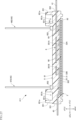
- FIG. 1 is a perspective view showing a semiconductor device according to a first embodiment of the present disclosure.
- FIG. 2 is a perspective view of main parts showing a semiconductor device according to a first embodiment of the present disclosure.
- FIG. 3 is a perspective view of a main part of a semiconductor device according to a first embodiment of the present disclosure.
- FIG. 4 is a plan view showing a semiconductor device according to the first embodiment of the present disclosure.
- FIG. 5 is a plan view of main parts showing the semiconductor device according to the first embodiment of the present disclosure.
- FIG. 6 is a side view of main parts showing a semiconductor device according to the first embodiment of the present disclosure.
- FIG. 7 is an enlarged plan view of a main part of the semiconductor device according to the first embodiment of the present disclosure.
- FIG. 1 is a perspective view showing a semiconductor device according to a first embodiment of the present disclosure.
- FIG. 2 is a perspective view of main parts showing a semiconductor device according to a first embodiment of the present disclosure.
- FIG. 3
- FIG. 8 is a plan view of main parts showing a semiconductor device according to the first embodiment of the present disclosure.
- FIG. 9 is a plan view of main parts showing a semiconductor device according to a first embodiment of the present disclosure.
- FIG. 10 is a side view showing the semiconductor device according to the first embodiment of the present disclosure.
- FIG. 11 is a bottom view of the semiconductor device according to the first embodiment of the present disclosure.
- FIG. 12 is a cross-sectional view taken along line XII-XII in FIG.
- FIG. 13 is a cross-sectional view taken along line XIII-XIII in FIG.
- FIG. 14 is an enlarged cross-sectional view of a main part of the semiconductor device according to the first embodiment of the present disclosure.
- FIG. 14 is an enlarged cross-sectional view of a main part of the semiconductor device according to the first embodiment of the present disclosure.
- FIG. 15 is an enlarged cross-sectional view of a main part of a semiconductor device according to a first embodiment of the present disclosure.
- FIG. 16 is a cross-sectional view taken along line XVI-XVI in FIG.
- FIG. 17 is a cross-sectional view taken along line XVII-XVII in FIG.
- FIG. 18 is a cross-sectional view taken along line XVIII-XVIII in FIG.
- FIG. 19 is a cross-sectional view taken along line XIX-XIX in FIG.
- FIG. 20 is a sectional view taken along line XX-XX in FIG. 5.
- FIG. 21 is a perspective view showing the second conductive member of the semiconductor device according to the first embodiment of the present disclosure.
- FIG. 22 is a plan view showing the second conductive member of the semiconductor device according to the first embodiment of the present disclosure.
- FIG. 23 is a front view showing the second conductive member of the semiconductor device according to the first embodiment of the present disclosure.
- FIG. 24 is an enlarged front view of main parts showing the second conductive member of the semiconductor device according to the first embodiment of the present disclosure.
- FIG. 25 is a side view showing the second conductive member of the semiconductor device according to the first embodiment of the present disclosure.
- FIG. 26 is a cross-sectional view showing a first modification of the semiconductor device according to the first embodiment of the present disclosure.
- FIG. 27 is a cross-sectional view showing a first modification of the semiconductor device according to the first embodiment of the present disclosure.
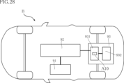
- FIG. 28 is a schematic diagram of a vehicle equipped with the semiconductor device of the present disclosure.
- a thing A is formed on a thing B and "a thing A is formed on a thing B” mean “a thing A is formed on a thing B” unless otherwise specified.
- "something A is placed on something B” and “something A is placed on something B” mean "something A is placed on something B” unless otherwise specified.
- a certain surface A faces (one side or the other side of) the direction B is not limited to the case where the angle of the surface A with respect to the direction B is 90 degrees; Including cases where it is tilted to the opposite direction.
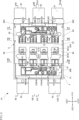
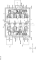
- the semiconductor device A1 of this embodiment includes a plurality of first semiconductor elements 10A, a plurality of second semiconductor elements 10B, a support substrate 3, a first terminal 41, a second terminal 42, a plurality of third terminals 43, and a fourth terminal 44. , a plurality of control terminals 45 , a control terminal support 48 , a first conduction member 5 , a second conduction member 6 , and a sealing resin 8 .
- FIG. 1 is a perspective view showing a semiconductor device A1.
- 2 and 3 are perspective views of essential parts of the semiconductor device A1.
- FIG. 4 is a plan view showing the semiconductor device A1.
- FIG. 5 is a plan view of essential parts of the semiconductor device A1.
- FIG. 6 is a side view of essential parts of the semiconductor device A1.
- FIG. 7 is an enlarged plan view of the main parts of the semiconductor device A1.
- 8 and 9 are principal part plan views showing the semiconductor device A1.
- FIG. 10 is a side view showing the semiconductor device A1.
- FIG. 11 is a bottom view showing the semiconductor device A1.
- FIG. 12 is a cross-sectional view taken along line XII-XII in FIG.
- FIG. 13 is a cross-sectional view taken along line XIII-XIII in FIG.
- FIG. 14 and 15 are enlarged cross-sectional views of essential parts of the semiconductor device A1.
- FIG. 16 is a cross-sectional view taken along line XVI-XVI in FIG.
- FIG. 17 is a cross-sectional view taken along line XVII-XVII in FIG.
- FIG. 18 is a cross-sectional view taken along line XVIII-XVIII in FIG.
- FIG. 19 is a cross-sectional view taken along line XIX-XIX in FIG.
- FIG. 20 is a sectional view taken along line XX-XX in FIG. 5.
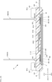
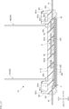
- FIG. 21 is a perspective view showing the second conductive member 6 of the semiconductor device A1.
- FIG. 22 is a plan view showing the second conductive member 6 of the semiconductor device A1.
- FIG. 21 is a perspective view showing the second conductive member 6 of the semiconductor device A1.
- FIG. 22 is a plan view showing the second conductive member 6 of the semiconductor device A1.
- FIG. 21 is a perspective view
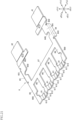
- FIG. 23 is a front view showing the second conductive member 6 of the semiconductor device A1.
- FIG. 24 is an enlarged front view of the main part showing the second conductive member of the semiconductor device A1.
- FIG. 25 is a side view showing the second conductive member 6 of the semiconductor device A1.
- the z direction is an example of the thickness direction of the present disclosure
- the x direction is an example of the first direction of the present disclosure
- the y direction is an example of the second direction of the present disclosure.
- one side in the x direction is referred to as the x1 side in the x direction
- the other side in the x direction is referred to as the x2 side in the x direction.
- one side in the y direction is referred to as the y1 side in the y direction
- the other side in the y direction is referred to as the y2 side in the y direction.
- one side in the z direction is referred to as a z1 side in the z direction
- the other side in the z direction is referred to as a z2 side in the z direction.
- the plurality of first semiconductor elements 10A and the plurality of second semiconductor elements 10B are each electronic components that serve as the functional center of the semiconductor device A1.
- the constituent material of each first semiconductor element 10A and each second semiconductor element 10B is, for example, a semiconductor material mainly composed of SiC (silicon carbide). This semiconductor material is not limited to SiC, and may be Si (silicon), GaN (gallium nitride), C (diamond), or the like.
- Each of the first semiconductor elements 10A and each of the second semiconductor elements 10B is a power semiconductor chip having a switching function, such as a MOSFET (Metal Oxide Semiconductor Field Effect Transistor).
- MOSFET Metal Oxide Semiconductor Field Effect Transistor
- first semiconductor element 10A and the second semiconductor element 10B are MOSFETs, but the present invention is not limited to this, and other transistors such as IGBTs (Insulated Gate Bipolar Transistors) can be used. There may be.
- Each first semiconductor element 10A and each second semiconductor element 10B are the same element.
- Each first semiconductor element 10A and each second semiconductor element 10B is, for example, an n-channel MOSFET, but may be a p-channel MOSFET.
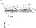
- the first semiconductor element 10A and the second semiconductor element 10B each have an element main surface 101 and an element back surface 102, as shown in FIGS. 14 and 15.
- the element main surface 101 and the element back surface 102 are separated in the z direction.
- the element main surface 101 faces the z1 side in the z direction
- the element back surface 102 faces the z2 side in the z direction.
- the semiconductor device A1 includes four first semiconductor elements 10A and four second semiconductor elements 10B, but the number of first semiconductor elements 10A and the number of second semiconductor elements 10B are different from each other. It is not limited to the configuration and may be changed as appropriate depending on the performance required of the semiconductor device A1. In the examples of FIGS. 8 and 9, four first semiconductor elements 10A and four second semiconductor elements 10B are arranged. The number of the first semiconductor elements 10A and the second semiconductor elements 10B may be two or three, or five or more each. The number of first semiconductor elements 10A and the number of second semiconductor elements 10B may be equal or different. The number of first semiconductor elements 10A and second semiconductor elements 10B is determined by the current capacity handled by semiconductor device A1.
- the semiconductor device A1 is configured, for example, as a half-bridge switching circuit.
- the plurality of first semiconductor elements 10A constitute an upper arm circuit of the semiconductor device A1
- the plurality of second semiconductor elements 10B constitute a lower arm circuit.
- the plurality of first semiconductor elements 10A are connected in parallel with each other
- the plurality of second semiconductor elements 10B are connected in parallel with each other.
- Each first semiconductor element 10A and each second semiconductor element 10B are connected in series and constitute a bridge layer.
- the plurality of first semiconductor elements 10A are each mounted on a first conductive portion 32A of the support substrate 3, which will be described later, as shown in FIGS. 8, 9, and 19.
- the plurality of first semiconductor elements 10A are arranged, for example, in the y direction and separated from each other.
- Each first semiconductor element 10A is conductively bonded to the first conductive portion 32A via a conductive bonding material 19.
- the element back surface 102 faces the first conductive part 32A.
- the plurality of first semiconductor elements 10A may be mounted on a metal member different from a part of the DBC substrate or the like. In this case, the metal member corresponds to the first conductive part in the present disclosure. This metal member may be supported by, for example, the first conductive portion 32A.
- the plurality of second semiconductor elements 10B are each mounted on a second conductive portion 32B of the support substrate 3, which will be described later, as shown in FIGS. 8, 9, and 18.
- the plurality of second semiconductor elements 10B are arranged, for example, in the y direction and separated from each other.
- Each second semiconductor element 10B is conductively bonded to the second conductive portion 32B via a conductive bonding material 19.
- the element back surface 102 faces the second conductive part 32B.
- the plurality of first semiconductor elements 10A and the plurality of second semiconductor elements 10B overlap, but they do not need to overlap.
- the plurality of second semiconductor elements 10B may be mounted on a metal member different from a part of the DBC substrate or the like.
- the metal member corresponds to the second conductive part in the present disclosure. This metal member may be supported, for example, by the second conductive portion 32B.
- the plurality of first semiconductor elements 10A and the plurality of second semiconductor elements 10B each have a first main surface electrode 11, a second main surface electrode 12, a third main surface electrode 13, and a back electrode 15.
- the configurations of the first main surface electrode 11, second main surface electrode 12, third main surface electrode 13, and back surface electrode 15 described below are common to each first semiconductor element 10A and each second semiconductor element 10B.
- the first main surface electrode 11, the second main surface electrode 12, and the third main surface electrode 13 are provided on the element main surface 101.
- the first main surface electrode 11, the second main surface electrode 12, and the third main surface electrode 13 are insulated by an insulating film (not shown).
- the back electrode 15 is provided on the back surface 102 of the element.
- the first principal surface electrode 11 is, for example, a gate electrode, and a drive signal (for example, gate voltage) for driving the first semiconductor element 10A (second semiconductor element 10B) is input.
- the second main surface electrode 12 is, for example, a source electrode, through which a source current flows.
- the second main surface electrode 12 of this embodiment has a gate finger 121.
- the gate finger 121 is made of, for example, a linear insulator extending in the x direction, and divides the second main surface electrode 12 into two in the y direction.
- the third main surface electrode 13 is, for example, a source sense electrode, through which a source current flows.
- the back electrode 15 is, for example, a drain electrode, through which a drain current flows.
- the back electrode 15 covers substantially the entire area of the back surface 102 of the element.
- the back electrode 15 is made of, for example, Ag (silver) plating.
- each first semiconductor element 10A (each second semiconductor element 10B) changes between a conductive state and a disconnected state according to this drive signal. The state changes. In a conductive state, a current flows from the back electrode 15 (drain electrode) to the second main surface electrode 12 (source electrode), and in a cutoff state, this current does not flow. That is, each first semiconductor element 10A (each second semiconductor element 10B) performs a switching operation.
- the semiconductor device A1 receives input between one fourth terminal 44 and two first terminals 41 and second terminals 42 due to the switching functions of the plurality of first semiconductor elements 10A and the plurality of second semiconductor elements 10B. For example, the DC voltage is converted into an AC voltage, and the AC voltage is output from the third terminal 43.
- the semiconductor device A1 includes a thermistor 17, as shown in FIGS. 5, 8, 9, etc.
- the thermistor 17 is used as a temperature detection sensor. Note that, in addition to the thermistor 17, the configuration may include, for example, a temperature-sensitive diode, or the configuration may not include the thermistor 17 or the like.
- the support substrate 3 supports the plurality of first semiconductor elements 10A and the plurality of second semiconductor elements 10B.
- the specific structure of the support substrate 3 is not limited at all, and may be formed of, for example, a DBC (Direct Bonded Copper) substrate or an AMB (Active Metal Brazing) substrate.
- Support substrate 3 includes an insulating layer 31, a first metal layer 32, and a back metal layer 33.
- the first metal layer 32 includes a first conductive part 32A and a second conductive part 32B.
- the dimension of the support substrate 3 in the z direction is, for example, 0.4 mm or more and 3.0 mm or less.
- the insulating layer 31 is made of, for example, ceramics with excellent thermal conductivity. Such ceramics include, for example, SiN (silicon nitride).
- the insulating layer 31 is not limited to ceramics, and may be an insulating resin sheet or the like.
- the insulating layer 31 has, for example, a rectangular shape in plan view.
- the dimension of the insulating layer 31 in the z direction is, for example, 0.05 mm or more and 1.0 mm or less.
- the first conductive part 32A supports the plurality of first semiconductor elements 10A
- the second conductive part 32B supports the plurality of second semiconductor elements 10B.
- the first conductive part 32A and the second conductive part 32B are formed on the upper surface of the insulating layer 31 (the surface facing the z1 side in the z direction).
- the constituent material of the first conductive part 32A and the second conductive part 32B includes, for example, Cu (copper).
- the constituent material may include, for example, Al (aluminum) other than Cu (copper).
- the first conductive part 32A and the second conductive part 32B are separated in the x direction.
- the first conductive part 32A is located on the x1 side of the second conductive part 32B in the x direction.
- the first conductive portion 32A and the second conductive portion 32B each have, for example, a rectangular shape in plan view.
- the first conductive part 32A and the second conductive part 32B, together with the first conductive member 5 and the second conductive member 6, are paths for the main circuit current switched by the plurality of first semiconductor elements 10A and the plurality of second semiconductor elements 10B. Configure.
- the first conductive part 32A has a first main surface 301A.
- the first main surface 301A is a plane facing the z1 side in the z direction.
- a plurality of first semiconductor elements 10A are each bonded to the first main surface 301A of the first conductive portion 32A via a conductive bonding material 19.
- the second conductive portion 32B has a second main surface 301B.
- the second main surface 301B is a plane facing the z1 side in the z direction.
- a plurality of second semiconductor elements 10B are bonded to the second main surface 301B of the second conductive portion 32B via a conductive bonding material 19.
- the constituent material of the conductive bonding material 19 is not particularly limited, and may be, for example, solder, metal paste material, or sintered metal.
- the dimensions of the first conductive part 32A and the second conductive part 32B in the z direction are, for example, 0.1 mm or more and 1.5 mm or less.
- the back metal layer 33 is formed on the lower surface of the insulating layer 31 (the surface facing the z2 side in the z direction).
- the constituent material of the back metal layer 33 is the same as that of the first metal layer 32.
- Back metal layer 33 has a back surface 302.
- the back surface 302 is a plane facing the z2 side in the z direction. In the example shown in FIG. 11, the back surface 302 is exposed from the sealing resin 8, for example.
- a heat dissipating member for example, a heat sink, etc. (not shown) can be attached to the back surface 302.
- the back surface 302 may not be exposed from the sealing resin 8 and may be covered with the sealing resin 8.
- the back metal layer 33 overlaps both the first conductive part 32A and the second conductive part 32B in plan view.
- the first terminal 41, the second terminal 42, the plurality of third terminals 43, and the fourth terminal 44 are each made of a plate-shaped metal plate.
- This metal plate includes, for example, Cu (copper) or a Cu (copper) alloy. In the examples shown in FIGS. 1 to 5, FIG. 8, FIG. 9, and FIG. However, the number of each terminal is not limited at all.
- a DC voltage to be subjected to power conversion is input to the first terminal 41, the second terminal 42, and the fourth terminal 44.
- the fourth terminal 44 is a positive electrode (P terminal), and the first terminal 41 and the second terminal 42 are each negative electrodes (N terminal).
- P terminal positive electrode
- N terminal negative electrodes
- the first terminal 41 , the second terminal 42 , the plurality of third terminals 43 , and the fourth terminal 44 each include a portion covered with the sealing resin 8 and a portion exposed from the sealing resin 8 .
- the fourth terminal 44 is electrically connected to the first conductive portion 32A.
- the method of conductive bonding is not limited at all, and methods such as ultrasonic bonding, laser bonding, welding, or methods using solder, metal paste, silver sintered body, etc. are appropriately employed.
- the fourth terminal 44 is located on the x1 side in the x direction with respect to the plurality of first semiconductor elements 10A and the first conductive portion 32A, as shown in FIGS. 8, 9, and the like.
- the fourth terminal 44 is electrically connected to the first conductive portion 32A and, via the first conductive portion 32A, to the back electrode 15 (drain electrode) of each first semiconductor element 10A.
- the first terminal 41 and the second terminal 42 are electrically connected to the second conductive member 6.
- the first terminal 41 and the second conductive member 6 are integrally formed.
- the first terminal 41 and the second conductive member 6 are integrally formed, for example, by cutting and bending a single metal plate material, and are joined together. Refers to a configuration that does not include any bonding materials, etc.
- the second terminal 42 and the second conductive member 6 are integrally formed. Note that the first terminal 41 and the second terminal 42 may have a structure as long as they are electrically connected to the second conductive member 6, and unlike this embodiment, they may have a structure that has a joint portion that joins them to each other.
- the first terminal 41 and the second terminal 42 are respectively located on the x1 side in the x direction with respect to the plurality of first semiconductor elements 10A and the first conductive portion 32A, as shown in FIGS. 5, 8, and the like.
- the first terminal 41 and the second terminal 42 are each electrically connected to the second conductive member 6 and connected to the second main surface electrode 12 (source electrode) of each second semiconductor element 10B via the second conductive member 6. Conduct.
- the first terminal 41, the second terminal 42, and the fourth terminal 44 each protrude from the sealing resin 8 toward the x1 side in the x direction in the semiconductor device A1.
- the first terminal 41, the second terminal 42, and the fourth terminal 44 are spaced apart from each other.
- the first terminal 41 and the second terminal 42 are located on opposite sides of the fourth terminal 44 in the y direction.
- the first terminal 41 is located on the y1 side of the fourth terminal 44 in the y direction
- the second terminal 42 is located on the y2 side of the fourth terminal 44 in the y direction.
- the first terminal 41, the second terminal 42, and the fourth terminal 44 overlap each other when viewed in the y direction.
- the two third terminals 43 are each electrically connected to the second conductive portion 32B.
- the method of conductive bonding is not limited at all, and methods such as ultrasonic bonding, laser bonding, welding, or methods using solder, metal paste, silver sintered body, etc. are appropriately employed.
- the two third terminals 43 are each located on the x2 side in the x direction with respect to the plurality of second semiconductor elements 10B and the second conductive portion 32B.
- Each third terminal 43 is electrically connected to the second conductive portion 32B and, via the second conductive portion 32B, to the back electrode 15 (drain electrode) of each second semiconductor element 10B.
- third terminals 43 is not limited to two, and may be one, for example, or three or more. For example, when there is only one third terminal 43, it is desirable that it is connected to the central portion of the second conductive portion 32B in the y direction.
- Each of the plurality of control terminals 45 is a pin-shaped terminal for controlling each first semiconductor element 10A and each second semiconductor element 10B.
- the plurality of control terminals 45 include a plurality of first control terminals 46A-46E and a plurality of second control terminals 47A-47D.
- the plurality of first control terminals 46A to 46E are used for controlling each first semiconductor element 10A.
- the plurality of second control terminals 47A to 47D are used for controlling each second semiconductor element 10B.
- the plurality of first control terminals 46A to 46E are arranged at intervals in the y direction. As shown in FIGS. 8, 13, and 20, each of the first control terminals 46A to 46E is supported by the first conductive portion 32A via a control terminal support 48 (a first support portion 48A to be described later). Ru. As shown in FIGS. 5 and 8, each of the first control terminals 46A to 46E is connected between the plurality of first semiconductor elements 10A and the first terminal 41, the second terminal 42, and the fourth terminal 44 in the x direction. Located in
- the first control terminal 46A is a terminal (gate terminal) for inputting a drive signal for the plurality of first semiconductor elements 10A.
- a drive signal for driving the plurality of first semiconductor elements 10A is input to the first control terminal 46A (for example, a gate voltage is applied).
- the first control terminal 46B is a source signal detection terminal (source sense terminal) of the plurality of first semiconductor elements 10A.
- the voltage (voltage corresponding to the source current) applied to each second main surface electrode 12 (source electrode) of the plurality of first semiconductor elements 10A is detected from the first control terminal 46B.
- the first control terminal 46C and the first control terminal 46D are terminals that are electrically connected to the thermistor 17.
- the first control terminal 46E is a drain signal detection terminal (drain sense terminal) of the plurality of first semiconductor elements 10A.
- the voltage (voltage corresponding to the drain current) applied to each back electrode 15 (drain electrode) of the plurality of first semiconductor elements 10A is detected from the first control terminal 46E.
- the plurality of second control terminals 47A to 47D are arranged at intervals in the y direction. As shown in FIGS. 8 and 13, each of the second control terminals 47A to 47D is supported by the second conductive portion 32B via a control terminal support 48 (second support portion 48B to be described later). Each of the second control terminals 47A to 47D is located between the plurality of second semiconductor elements 10B and the two third terminals 43 in the x direction, as shown in FIGS. 5 and 8.
- the second control terminal 47A is a terminal (gate terminal) for inputting drive signals for the plurality of second semiconductor elements 10B.
- a drive signal for driving the plurality of second semiconductor elements 10B is input to the second control terminal 47A (for example, a gate voltage is applied).
- the second control terminal 47B is a terminal (source sense terminal) for detecting source signals of the plurality of second semiconductor elements 10B.
- the voltage (voltage corresponding to the source current) applied to each second main surface electrode 12 (source electrode) of the plurality of second semiconductor elements 10B is detected from the second control terminal 47B.
- the second control terminal 47C and the second control terminal 47D are terminals that are electrically connected to the thermistor 17.
- Each of the plurality of control terminals 45 (the plurality of first control terminals 46A to 46E and the plurality of second control terminals 47A to 47D) includes a holder 451 and a metal pin 452.
- the holder 451 is made of a conductive material. As shown in FIGS. 14 and 15, the holder 451 is bonded to the control terminal support 48 (first metal layer 482, which will be described later) via a conductive bonding material 459.
- the holder 451 includes a cylindrical portion, an upper end flange, and a lower end flange. The upper end flange is connected above the cylindrical part, and the lower end flange is connected below the cylindrical part.
- a metal pin 452 is inserted through at least the upper end flange and the cylindrical portion of the holder 451 .
- the holder 451 is covered with a sealing resin 8 (a second protrusion 852 to be described later).
- the metal pin 452 is a rod-shaped member extending in the z direction.
- the metal pin 452 is supported by being press-fitted into the holder 451.
- the metal pin 452 is electrically connected to the control terminal support 48 (first metal layer 482 described below) through at least the holder 451.
- the control terminal support 48 first metal layer 482 described below
- the metal pin 452 is electrically connected to the control terminal support 48 via a conductive bonding material 459.
- the control terminal support 48 supports the plurality of control terminals 45.
- the control terminal support body 48 is interposed between the first main surface 301A and the second main surface 301B and the plurality of control terminals 45 in the z direction.
- the control terminal support 48 includes a first support portion 48A and a second support portion 48B.
- the first support portion 48A is disposed on the first conductive portion 32A and supports a plurality of first control terminals 46A to 46E among the plurality of control terminals 45.
- the first support portion 48A is bonded to the first conductive portion 32A via a bonding material 49, as shown in FIG.
- the bonding material 49 may be conductive or insulating, and for example, solder is used.
- the second support portion 48B is disposed on the second conductive portion 32B and supports a plurality of second control terminals 47A to 47D among the plurality of control terminals 45.
- the second support portion 48B is bonded to the second conductive portion 32B via a bonding material 49, as shown in FIG.
- the control terminal support body 48 (each of the first support part 48A and the second support part 48B) is composed of, for example, a DBC (Direct Bonded Copper) board.
- the control terminal support 48 includes an insulating layer 481, a first metal layer 482, and a second metal layer 483 that are stacked on each other.
- the insulating layer 481 is made of ceramics, for example.
- the insulating layer 481 has, for example, a rectangular shape in plan view.
- the first metal layer 482 is formed on the upper surface of the insulating layer 481, as shown in FIGS. 14, 15, etc. Each control terminal 45 is erected on the first metal layer 482.
- the first metal layer 482 includes, for example, Cu (copper) or a Cu (copper) alloy. As shown in FIG. 8 and the like, the first metal layer 482 includes a first portion 482A, a second portion 482B, a third portion 482C, a fourth portion 482D, a fifth portion 482E, and a sixth portion 482F.
- the first portion 482A, the second portion 482B, the third portion 482C, the fourth portion 482D, the fifth portion 482E, and the sixth portion 482F are spaced apart and insulated from each other.
- the first portion 482A is connected to a plurality of wires 71 and is electrically connected to the first main surface electrode 11 (gate electrode) of each first semiconductor element 10A (each second semiconductor element 10B) via each wire 71.
- a plurality of wires 73 are connected to the first portion 482A and the sixth portion 482F.
- the sixth portion 482F is electrically connected to the first main surface electrode 11 (gate electrode) of each first semiconductor element 10A (each second semiconductor element 10B) via the wire 73 and the wire 71.
- the first control terminal 46A is connected to the sixth portion 482F of the first support portion 48A
- the second control terminal 47A is connected to the sixth portion 482F of the second support portion 48B. It is joined.
- the second portion 482B has a plurality of wires 72 joined and is electrically connected to the third main surface electrode 13 (source sense electrode) of each first semiconductor element 10A (each second semiconductor element 10B) via each wire 72.
- the first control terminal 46B is connected to the second portion 482B of the first support portion 48A
- the second control terminal 47B is connected to the second portion 482B of the second support portion 48B. It is joined.
- the thermistor 17 is joined to the third portion 482C and the fourth portion 482D.
- first control terminals 46C and 46D are connected to the third portion 482C and fourth portion 482D of the first support portion 48A
- the third portion 482C and the fourth portion 482D of the second support portion 48B are Second control terminals 47C and 47D are connected to the fourth portion 482D.
- a wire 74 is joined to the fifth portion 482E of the first support portion 48A, and the fifth portion 482E is electrically connected to the first conductive portion 32A via the wire 74. As shown in FIG. 8, the first control terminal 46E is joined to the fifth portion 482E of the first support portion 48A. The fifth portion 482E of the second support portion 48B is not electrically connected to other components.
- Each of the wires 71 to 74 described above is, for example, a bonding wire.
- the constituent material of each wire 71 to 74 includes, for example, one of Au (gold), Al (aluminum), or Cu (copper).
- the second metal layer 483 is formed on the lower surface of the insulating layer 481, as shown in FIGS. 14, 15, etc.
- the second metal layer 483 of the first support portion 48A is bonded to the first conductive portion 32A via a bonding material 49, as shown in FIG.
- the second metal layer 483 of the second support portion 48B is bonded to the second conductive portion 32B via a bonding material 49, as shown in FIG.
- the first conductive member 5 and the second conductive member 6 are spaced apart from the first main surface 301A and the second main surface 301B toward the z1 side in the z direction, and are separated from the first main surface 301A and the second main surface 301B in a plan view. overlaps with In this embodiment, the first conductive member 5 and the second conductive member 6 are each made of a metal plate.
- the metal includes, for example, Cu (copper) or a Cu (copper) alloy.
- the first conductive member 5 and the second conductive member 6 are appropriately bent metal plates.
- the first conductive member 5 is connected to the second main surface electrode 12 (source electrode) of each first semiconductor element 10A and the second conductive part 32B, and is connected to the second main surface electrode 12 (source electrode) of each first semiconductor element 10A and the second conductive part 32B. 2 conductive portion 32B.
- the first conductive member 5 constitutes a path for main circuit current switched by the plurality of first semiconductor elements 10A.
- the first conductive member 5 includes a main portion 51, a plurality of first joints 52, and a plurality of second joints 53, as shown in FIGS. 7 and 8.
- the main portion 51 is a band-shaped portion that is located between the plurality of first semiconductor elements 10A and the second conductive portion 32B in the x direction and extends in the y direction in a plan view.
- the main portion 51 overlaps both the first conductive portion 32A and the second conductive portion 32B in a plan view, and is spaced from the first main surface 301A and the second main surface 301B in the z direction toward the z1 side in the z direction.
- the main portion 51 is located on the z2 side in the z direction with respect to a third path portion 66 and a fourth path portion 67 of the second conductive member 6, which will be described later, and is located on the z2 side in the z direction. It is located closer to the first main surface 301A and the second main surface 301B than the fourth path portion 67 is.
- the main portion 51 is arranged parallel (or substantially parallel) to the first main surface 301A and the second main surface 301B.
- the main portion 51 extends continuously in the y direction corresponding to the region where the plurality of first semiconductor elements 10A are arranged.
- a plurality of first openings 514 are formed in the main portion 51.
- Each of the plurality of first openings 514 is, for example, a through hole penetrating in the z direction (thickness direction of the main portion 51).
- the plurality of first openings 514 are arranged at intervals in the y direction.
- the plurality of first openings 514 are provided corresponding to each of the plurality of first semiconductor elements 10A.
- the main portion 51 is provided with four first openings 514, and these first openings 514 and the plurality of (four) first semiconductor elements 10A are at the same position in the y direction.
- each first opening 514 overlaps the gap between the first conductive part 32A and the second conductive part 32B in plan view.
- the plurality of first openings 514 are arranged so that the upper side (z1 side in the z direction) and the It is formed to facilitate the flow of the resin material between the lower side (z2 side in the z direction).
- each first joint portion 52 and the plurality of second bonding portions 53 are each connected to the main portion 51 and are arranged corresponding to the plurality of first semiconductor elements 10A.
- each first joint portion 52 is located on the x1 side in the x direction with respect to the main portion 51.
- Each second joint portion 53 is located on the x2 side of the main portion 51 in the x direction.
- each first bonding portion 52 and the corresponding second main surface electrode 12 of one of the first semiconductor elements 10A are bonded via a conductive bonding material 59.
- Each second joint portion 53 and the second conductive portion 32B are joined via a conductive joining material 59.
- the constituent material of the conductive bonding material 59 is not particularly limited, and may be, for example, solder, metal paste material, or sintered metal.
- the first joint portion 52 has two portions spaced apart in the y direction. These two parts are joined to the second main surface electrode 12 on both sides in the y direction, with the gate fingers 121 of the second main surface electrode 12 of the first semiconductor element 10A interposed therebetween.
- the second conductive member 6 connects the second main surface electrode 12 (source electrode) of each second semiconductor element 10B to the first terminal 41 and the second terminal 42.
- the second conductive member 6 is integrally formed with the first terminal 41 and the second terminal 42.
- the second conductive member 6 constitutes a path for main circuit current switched by the plurality of second semiconductor elements 10B. As shown in FIG. 7 and FIG. 21 to FIG. A path section 67 is included. Further, in the illustrated example, the second conductive member 6 includes a first step portion 602 and a second step portion 603.
- the plurality of third bonding parts 61 are parts that are individually bonded to the plurality of second semiconductor elements 10B.
- Each third bonding portion 61 and the second main surface electrode 12 of each second semiconductor element 10B are bonded via a conductive bonding material 69.
- the constituent material of the conductive bonding material 69 is not particularly limited, and may be, for example, solder, metal paste material, or sintered metal.
- the third joint portion 61 has two flat portions 611 and two first inclined portions 612.
- the two flat parts 611 are lined up in the y direction.
- the two flat parts 611 are spaced apart from each other in the y direction.
- the shape of the flat portion 611 is not limited at all, and in the illustrated example, it is rectangular.
- the two flat parts are joined to the second main surface electrode 12 on both sides in the y direction, with the gate finger 121 of the second main surface electrode 12 of the second semiconductor element 10B interposed therebetween.
- the two first inclined parts 612 are connected to the outside of the two flat parts 611 in the y direction. That is, the first inclined portion 612 located on the y1 side in the y direction is connected to the y1 side in the y direction with respect to the flat portion 611 located on the y1 side in the y direction. Further, the first inclined portion 612 located on the y2 side in the y direction is connected to the y2 side in the y direction with respect to the flat portion 611 located on the y2 side in the y direction.
- the first inclined portion 612 is inclined so that the farther it is from the flat portion 611 in the y direction, the closer it is to the z1 side in the z direction.
- the first path portion 64 is interposed between the plurality of third joint portions 61 and the first terminal 41.
- the first path section 64 is connected to the first terminal 41 via the first step section 602.
- the first path portion 64 overlaps the first conductive portion 32A in plan view.
- the first path portion 64 has a shape that extends in the x direction as a whole.
- the first path portion 64 includes a first strip portion 641 and a first extension portion 643.
- the first strip portion 641 is located on the x2 side in the x direction with respect to the first terminal 41, and is substantially parallel to the first main surface 301A.
- the first strip portion 641 has a shape that extends in the x direction as a whole.
- the first strip 641 has a recess 649 .
- the recessed portion 649 is a portion where a portion of the first strip portion 641 is recessed toward the y1 side in the y direction. In FIG. 5, the first metal part 35 is exposed through the recess 649.
- the first extending portion 643 extends from the side end of the first strip portion 641 on the y1 side in the y direction to the z2 side in the z direction.
- the first extending portion 643 is spaced apart from the first conductive portion 32A.
- the first extending portion 643 has a shape along the z direction, and has an elongated rectangular shape whose longitudinal direction is the x direction. Note that the first path portion 64 may be configured without the first extending portion 643.
- the second path portion 65 is interposed between the plurality of third joint portions 61 and the second terminal 42.
- the second path section 65 is connected to the second terminal 42 via the second step section 603.
- the second path portion 65 overlaps the first conductive portion 32A in plan view.
- the second path portion 65 has a shape that extends in the x direction as a whole.
- the second path portion 65 includes a second strip portion 651 and a second extension portion 653.
- the second strip portion 651 is located on the x2 side in the x direction with respect to the second terminal 42, and is substantially parallel to the first main surface 301A.
- the second strip portion 651 has a shape that extends in the x direction as a whole.
- the second strip portion 651 has a recess 659 .
- the recessed portion 659 is a portion of the second strip portion 651 that is recessed toward the y2 side in the y direction. In FIG. 5, the second metal portion 36 is exposed through the recess 659.
- the second extending portion 653 extends from the side end of the second strip portion 651 on the y2 side in the y direction to the z2 side in the z direction.
- the second extending portion 653 is spaced apart from the first conductive portion 32A.
- the second extending portion 653 has a shape along the z direction, and has an elongated rectangular shape whose longitudinal direction is the x direction. Note that the second path portion 65 may be configured without the second extension portion 653.
- the configuration regarding the first path section 64 is, for example, in a line-symmetrical relationship with respect to a center line extending in the x direction,
- the second path section 65 can also be appropriately adopted.
- the plurality of third path portions 66 are individually connected to the plurality of third joint portions 61.
- Each of the third path sections 66 has a shape extending in the x direction, and is arranged to be spaced apart from each other in the y direction.
- the number of the plurality of third path sections 66 is not limited at all, and in the illustrated example, five third path sections 66 are arranged.
- Each third path section 66 is arranged to be located between the plurality of second semiconductor elements 10B in the y direction or to be located outside of the plurality of second semiconductor elements 10B in the y direction. .
- Concave portions 669 are formed in the two third path portions 66 located on both outer sides in the y direction.
- the recess 669 is recessed from the inside to the outside in the y direction.
- one recess 669 is formed in each of the two third path sections 66.
- the second conductive portion 32B is exposed through these recesses 669.
- one third joint portion 61 is arranged between two third path portions 66 adjacent to each other in the y direction.
- the first inclined part 612 located on the y1 side in the y direction is the third route part located on the y1 side in the y direction among the two third route parts 66 adjacent in the y direction. It is connected to 66.
- the first inclined portion 612 located on the y2 side in the y direction is the third path portion 612 located on the y2 side in the y direction among the two third path portions 66 adjacent in the y direction. It is connected to 66.
- the fourth path portion 67 is connected to the end of the plurality of third path portions 66 on the x1 side in the x direction.
- the fourth path portion 67 has a shape that extends long in the y direction.
- the fourth path portion 67 is connected to the ends of the first band portion 641 of the first path portion 64 and the second band portion 651 of the second path portion 65 on the x2 side in the x direction.
- the first path portion 64 is connected to the end of the fourth path portion 67 on the y1 side in the y direction.
- the second path portion 65 is connected to the end of the fourth path portion 67 on the y2 side in the y direction.
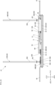
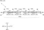
- the positions of the flat portions 611 of the plurality of third bonding portions 61 in the z direction are set in accordance with the curvature of the support substrate 3. More specifically, as shown in FIG. 23, the positions of the plurality of third path sections 66 in the z direction are the same (or substantially the same). Further, the positions of the plurality of third path portions 66 and the fourth path portions 67 in the z direction are the same (or substantially the same). The distance Gz in the z direction between the flat portions 611 of the plurality of third joints 61 and the fifth joints 63 is set in accordance with the curvature of the support substrate 3.
- the distance Gz1, the distance Gz2, the distance Gz3, and the distance Gz4 are set in order from the distance Gz of the third joint 61 located on the y2 side in the y direction.
- the curved imaginary line in the figure shows the curved shape of the curved second main surface 301B of the support substrate 3 in an exaggerated manner for convenience of understanding.
- the second main surface 301B is curved such that the center portion in the y direction is located on the z2 side in the z direction, and both end portions in the y direction are located on the z1 side in the z direction.
- distance Gz1 is smaller than distance Gz2.
- the distance Gz4 is smaller than the distance Gz3.
- the distance Gz1 and the distance Gz4 are, for example, substantially the same, and the distance Gz2 and the distance Gz3 are substantially the same.
- the difference between the distance Gz1 and the distance Gz2 is, for example, about 40 ⁇ m.
- the difference between the distances Gz3 and Gz4 is, for example, about 40 ⁇ m.
- the thickness of the conductive bonding material 69 is, for example, 60 ⁇ m or more and 120 ⁇ m or less. Note that the magnitude relationship between the distances Gz1 to Gz4 is appropriately set depending on the direction and amount of curvature of the support substrate 3 (second main surface 301B).
- the thickness t2 of the first inclined portion 612 is thinner than the thickness t1 of the flat portion 611. Further, the thickness t2 of the first inclined portion 612 is thinner than the thickness t0 of the third path portion 66. Further, the thickness t1 of the flat portion 611 and the thickness t0 of the third path portion 66 are the same (or substantially the same).
- an intermediate portion that will become the flat portion 611 and the first inclined portion 612 is formed in a metal plate material by cutting or the like.
- one third joint portion 61 is formed by two intermediate portions.
- a gap 619 is provided between these two intermediate portions.
- the gap 619 is a portion where the gate finger 121 of the second main surface electrode 12 of the second semiconductor element 10B is positioned. Therefore, the size of the gap 619 is set to be approximately the same as or slightly larger than the y-direction dimension of the gate finger 121, for example.
- the portions that will become the two flat portions 611 are sandwiched between, for example, a mold, and moved toward the z2 side in the z direction with respect to the third path portion 66 and the fourth path portion 67.
- a portion of each of the two intermediate portions has an inclined shape, forming two first inclined portions 612.
- the portion that becomes the first inclined portion 612 is subjected to tensile processing. Therefore, the thickness t2 is thinner than the thickness t1 and the thickness t0.
- the dimension of the gap 619 in the y direction hardly changes before and after moving the mold toward the z2 side in the z direction.
- the magnitudes of the distances Gz1 to Gz4 described above can be adjusted, for example, by the amount by which the mold is moved.
- the sealing resin 8 includes a plurality of first semiconductor elements 10A, a plurality of second semiconductor elements 10B, a support substrate 3 (excluding the back surface 302), a first terminal 41, a second terminal 42, and a plurality of third terminals. 43, a portion of each of the fourth terminals 44, a portion of each of the plurality of control terminals 45, the control terminal support 48, the first conduction member 5, the second conduction member 6, and the plurality of wires 71 to 43.
- the wires 74 and 74 are respectively covered.
- the sealing resin 8 is made of, for example, black epoxy resin.
- the sealing resin 8 is formed by, for example, molding.
- the sealing resin 8 has, for example, a dimension in the x direction of about 35 mm to 60 mm, a dimension in the y direction, for example, about 35 mm to 50 mm, and a dimension in the z direction, for example, about 4 mm to 15 mm. These dimensions are the largest along each direction.
- the sealing resin 8 has a resin main surface 81, a resin back surface 82, and a plurality of resin side surfaces 831 to 834.
- the resin main surface 81 and the resin back surface 82 are separated in the z direction, as shown in FIGS. 10, 12, and 18.
- the main resin surface 81 faces the z1 side in the z direction
- the resin back surface 82 faces the z2 side in the z direction.
- a plurality of control terminals 45 protrude from the main resin surface 81.
- the resin back surface 82 has a frame shape that surrounds the back surface 302 of the support substrate 3 (the lower surface of the back metal layer 33) in plan view.
- the back surface 302 of the support substrate 3 is exposed from the resin back surface 82, and is flush with the resin back surface 82, for example.
- Each of the plurality of resin side surfaces 831 to 834 is connected to both the resin main surface 81 and the resin back surface 82, and is sandwiched between them in the z direction. As shown in FIG. 4 and the like, the resin side surface 831 and the resin side surface 832 are separated from each other in the x direction.
- the resin side surface 831 faces the x2 side in the x direction
- the resin side surface 832 faces the x1 side in the x direction.
- Two third terminals 43 protrude from the resin side surface 831, and a first terminal 41, a second terminal 42, and a fourth terminal 44 protrude from the resin side surface 832.
- the resin side surface 833 and the resin side surface 834 are separated from each other in the y direction.
- the resin side surface 833 faces the y2 side in the y direction
- the resin side surface 834 faces the y1 side in the y direction.
- a plurality of recesses 832a are formed in the resin side surface 832.
- Each recessed portion 832a is a portion depressed in the x direction in plan view.
- the plurality of recesses 832a include those formed between the first terminal 41 and the fourth terminal 44 and those formed between the second terminal 42 and the fourth terminal 44 in plan view.
- the plurality of recesses 832a are provided to increase the creepage distance along the resin side surface 832 between the first terminal 41 and the fourth terminal 44, and the creepage distance along the resin side surface 832 between the second terminal 42 and the fourth terminal 44. It is provided.
- the sealing resin 8 has a plurality of first protrusions 851, a plurality of second protrusions 852, and a resin cavity 86, as shown in FIGS. 12 and 13.
- Each of the plurality of first protrusions 851 protrudes from the main resin surface 81 in the z direction.
- the plurality of first protrusions 851 are arranged near the four corners of the sealing resin 8 in plan view.
- a first protrusion end surface 851a is formed at the tip of each first protrusion 851 (end on the z1 side in the z direction).
- Each first protruding end surface 851a of the plurality of first protrusions 851 is substantially parallel to the main resin surface 81 and on the same plane (xy plane).
- Each first protrusion 851 is, for example, shaped like a hollow truncated cone with a bottom.
- the plurality of first protrusions 851 are used as spacers when the semiconductor device A1 is mounted on a control circuit board or the like of a device that uses a power source generated by the semiconductor device A1.
- Each of the plurality of first protrusions 851 has a recess 851b and an inner wall surface 851c formed in the recess 851b.
- the shape of each first protrusion 851 may be columnar, and is preferably columnar.
- the recess 851b has a cylindrical shape
- the inner wall surface 851c has a single perfect circular shape when viewed from above.
- the semiconductor device A1 may be mechanically fixed to a control circuit board or the like by a method such as screwing.
- a female thread can be formed on the inner wall surface 851c of the recess 851b in the plurality of first protrusions 851.
- Insert nuts may be embedded in the recesses 851b of the plurality of first protrusions 851.
- the plurality of second protrusions 852 protrude from the main resin surface 81 in the z direction, as shown in FIG. 13 and the like.
- the plurality of second protrusions 852 overlap the plurality of control terminals 45 in plan view.
- Each metal pin 452 of the plurality of control terminals 45 protrudes from each second protrusion 852 .
- Each second protrusion 852 has a truncated cone shape.
- the second protrusion 852 covers the holder 451 and a portion of the metal pin 452 at each control terminal 45 .
- the first terminal 41 and the second conductive member 6 are integrally formed. Thereby, compared to a configuration in which the first terminal 41 and the second conductive member 6 are joined, it is possible to reduce the number of joining steps in the manufacturing process of the semiconductor device A1. Moreover, it is possible to avoid cracking, peeling, etc. from occurring at the bonded portion when the semiconductor device A1 is used. Therefore, it is possible to simplify the manufacturing process of the semiconductor device A1 or improve its reliability during use.
- the second terminal 42 and the second conductive member 6 are integrally formed. Thereby, compared to a configuration in which the second terminal 42 and the second conductive member 6 are joined, it is possible to reduce the number of joining steps in the manufacturing process of the semiconductor device A1. Moreover, it is possible to avoid cracking, peeling, etc. from occurring at the bonded portion when the semiconductor device A1 is used. Therefore, it is possible to simplify the manufacturing process of the semiconductor device A1 or improve its reliability during use.
- the second conductive member 6 has a first stepped portion 602 connected to the first terminal 41. Thereby, the rigidity of the connecting portion between the second conductive member 6 and the first terminal 41 can be increased.
- the second conductive member 6 has a second stepped portion 603 connected to the second terminal 42. Thereby, the rigidity of the connecting portion between the second conductive member 6 and the second terminal 42 can be increased.
- the third joint part 61 has two flat parts 611 and two first slope parts 612.
- the two first inclined parts 612 are connected to the outside of the two flat parts 611 in the y direction. Therefore, the current flowing through the second main surface electrode 12 flows from the second main surface electrode 12 to both sides in the y direction via the flat part 611 and the first slope part 612. Thereby, it is possible to suppress the current flowing through the second main surface electrode 12 from concentrating in one place.
- the two flat parts 611 are separated in the y direction. This allows current to flow reliably through both the two flat parts 611 and the two first slope parts 612, which is preferable for suppressing current concentration.
- the gate finger 121 of the second main surface electrode 12 can be placed between them.
- One third joint portion 61 is arranged between two third path portions 66 adjacent in the y direction. Thereby, it is possible to distribute the current flowing through the second main surface electrode 12 of one second semiconductor element 10B to the two third path sections 66.
- the positions of the flat portions 611 of the plurality of third bonding portions 61 in the z direction are set in accordance with the curvature of the support substrate 3 (second main surface 301B). Thereby, it is possible to make the distances in the z direction between the flat portions 611 of the plurality of third bonding portions 61 and the second main surface electrodes 12 of the plurality of second semiconductor elements 10B more uniform.
- the thickness of the conductive bonding material 69 that joins the second principal surface electrode 12 of one of the second semiconductor elements 10B and the flat portion 611 of the third bonding portion 61 becomes unduly thin, and the conductive It is possible to suppress the occurrence of cracks and peeling in the bonding material 69, and it is possible to suppress shortening of the product life.
- the distance Gz in the z direction between the flat portions 611 of the plurality of third joint portions 61 and the third path portion 66 is set in accordance with the curvature of the support substrate 3 (second main surface 301B).
- the third path portion 66, the fourth path portion 67, etc. are formed into a flat shape, for example, regardless of the curvature of the support substrate 3, and when the plurality of third joint portions 61 are formed, the third path portion 66, the fourth path portion 67, etc. , the curvature of the support substrate 3 may be considered.
- the thickness t2 of the first inclined portion 612 is thinner than the thickness t1 of the flat portion 611.
- Such a configuration can be formed by the above-mentioned tensile processing using a mold. In this case, there is an advantage that the size of the gap 619 can be easily controlled to a desired size.
- 26 and 27 show a modification of the present disclosure.
- the same or similar elements as in the above embodiment are given the same reference numerals as in the above embodiment.
- the configurations of each part in each modification and each embodiment can be combined with each other as appropriate within a range that does not cause technical contradiction.
- 26 and 27 show a first modification of the semiconductor device A1.
- the second conductive member 6 does not have the above-described first step portion 602 and second step portion 603.
- the position of the first terminal 41 in the z-direction is the same (or substantially the same) as the position of the first strip portion 641 of the first path portion 64 in the z-direction. That is, the first terminal 41 and the first strip portion 641 are connected to form an integral flat plate.
- the position of the second terminal 42 in the z-direction is the same (or substantially the same) as the position of the second strip portion 651 of the second path portion 65 in the z-direction. That is, the second terminal 42 and the second strip portion 651 are connected to form an integral flat plate.
- the specific shape of the connecting portion between the second conductive member 6, the first terminal 41, and the second terminal 42 is not limited at all.
- Vehicle B is, for example, an electric vehicle (EV).
- EV electric vehicle
- vehicle B includes an on-vehicle charger 91, a storage battery 92, and a drive system 93.
- Electric power is wirelessly supplied to the on-vehicle charger 91 from a power supply facility (not shown) installed outdoors.
- the means for supplying power from the power supply facility to the on-vehicle charger 91 may be wired.
- the on-vehicle charger 91 includes a step-up DC-DC converter.
- the voltage of the power supplied to the on-vehicle charger 91 is boosted by the converter and then supplied to the storage battery 92 .
- the boosted voltage is, for example, 600V.
- the drive system 93 drives the vehicle B.
- Drive system 93 includes an inverter 931 and a drive source 932.
- Semiconductor device A10 constitutes a part of inverter 931.
- the power stored in the storage battery 92 is supplied to the inverter 931.
- the power supplied from the storage battery 92 to the inverter 931 is DC power.
- a step-up DC-DC converter may be further provided between the storage battery 92 and the inverter 931.
- Inverter 931 converts DC power into AC power.
- the inverter 931 including the semiconductor device A10 is electrically connected to a drive source 932.
- Drive source 932 includes an AC motor and a transmission.
- the AC motor rotates and the rotation is transmitted to the transmission.
- the transmission rotates the drive shaft of vehicle B after appropriately reducing the number of rotations transmitted from the AC motor.
- vehicle B is driven.
- the semiconductor device A10 in the inverter 931 is necessary to output AC power whose frequency is appropriately changed in order to correspond to the required rotational speed of the AC motor.
- the semiconductor device according to the present disclosure is not limited to the embodiments described above.
- the specific configuration of each part of the semiconductor device according to the present disclosure can be changed in design in various ways.
- the present disclosure includes the embodiments described in the appendix below.
- a first conductive portion having a first main surface facing one side in the thickness direction and located on one side in a first direction perpendicular to the thickness direction; and a second main surface facing one side in the thickness direction.
- a support substrate having a second conductive portion having a surface and located on the other side in the first direction; a plurality of first semiconductor elements mounted on the first conductive part and each having a switching function; a plurality of second semiconductor elements mounted on the second conductive part and each having a switching function; a first terminal protruding toward one side in the first direction with respect to the first conductive part; a first conductive member that connects the plurality of first semiconductor elements and the second conductive part; a second conductive member that connects the plurality of second semiconductor elements and the first terminal; a sealing resin that covers the plurality of first semiconductor elements, the plurality of second semiconductor elements, the first conductive member and the second conductive member, and a portion of each of the support substrate and the first terminal; Equipped with In the semiconductor device, the first terminal
- Appendix 2 a second terminal protruding to one side in the first direction with respect to the first conductive part and located on the other side in a second direction perpendicular to the thickness direction and the first direction with respect to the first terminal; More prepared, The semiconductor device according to appendix 1, wherein the second terminal and the second conductive member are integrally formed. Appendix 3.
- the first conductive member has a plurality of first joint parts joined to the plurality of first semiconductor elements, and a second joint part joined to the second conductive part
- the second conductive member includes a plurality of third joint parts joined to the plurality of second semiconductor elements, a first path part interposed between the plurality of third joint parts and the first terminal, and a first path part interposed between the plurality of third joint parts and the first terminal;
- the semiconductor device according to supplementary note 2 comprising a plurality of third joint portions and a second path portion interposed between the second terminals.
- Appendix 4 The semiconductor device according to appendix 3, wherein the second conductive member has a first stepped portion interposed between the first terminal and the first path portion. Appendix 5.
- Appendix 6. The semiconductor device according to appendix 3, wherein the first terminal and the first path portion are at the same position in the thickness direction.
- Appendix 7. The semiconductor device according to appendix 6, wherein the second terminal and the second path portion are at the same position in the thickness direction.
- Appendix 8. Supplementary Notes 3 to 7, wherein the first path portion has a first strip portion extending in the first direction and a first extending portion extending from the first strip portion to the other side in the thickness direction.
- the second path portion includes a second strip portion extending in the first direction and a second extending portion extending from the second strip portion to the other side in the thickness direction.
- semiconductor devices Appendix 10.
- the second conductive member includes a plurality of third path portions each extending in the first direction, one side end in the first direction of the plurality of third path portions, the first path portion, and the second path. 10.
- the semiconductor device according to any one of appendices 3 to 9, further comprising a fourth path portion connected to the fourth path portion and extending in the second direction.
- the third bonding portion includes two flat portions each connected to the second semiconductor element and arranged in the second direction, and two flat portions connected to the outside in the second direction with respect to the two flat portions. 1.
- the semiconductor device according to appendix 10 comprising: 1 inclined portion. Appendix 12. The semiconductor device according to attachment 11, wherein the first inclined portion extends from the third path portion in the second direction when viewed in the thickness direction. Appendix 13. The semiconductor device according to appendix 12, wherein the first sloped portion has a thickness that is equal to or less than the thickness of the flat portion. Appendix 14. 14. The semiconductor device according to appendix 13, wherein the first inclined portion has a thickness that is less than or equal to the third path portion. Appendix 15. 15. The semiconductor device according to appendix 14, wherein the thickness of the flat portion and the thickness of the third path portion are the same. Appendix 16.
- the first bonding portion has two flat portions, each of which is bonded to the first semiconductor element and arranged in the second direction, At least one of the positions of the flat parts of the plurality of first joint parts in the thickness direction and the positions of the flat parts of the plurality of third joint parts in the thickness direction are determined by the curvature of the support substrate.
- a driving source A semiconductor device according to any one of Supplementary Notes 1 to 17, The vehicle, wherein the semiconductor device is electrically connected to the drive source.
Landscapes
- Engineering & Computer Science (AREA)
- Microelectronics & Electronic Packaging (AREA)
- Power Engineering (AREA)
- Physics & Mathematics (AREA)
- Condensed Matter Physics & Semiconductors (AREA)
- General Physics & Mathematics (AREA)
- Computer Hardware Design (AREA)
- Cooling Or The Like Of Semiconductors Or Solid State Devices (AREA)
Abstract
Ce dispositif à semi-conducteur comprend : un substrat de support qui comporte une première partie conductrice et une seconde partie conductrice ; une pluralité de premiers éléments semi-conducteurs qui possèdent chacun une fonction de commutation et qui sont montés sur la première partie conductrice ; une pluralité de seconds éléments semi-conducteurs qui possèdent chacun une fonction de commutation et qui sont montés sur la seconde partie conductrice ; une première borne qui fait saillie vers le côté x1 de la direction x par rapport à la première partie conductrice ; un premier élément conducteur qui connecte électriquement la pluralité de premiers éléments semi-conducteurs et la seconde partie conductrice ; un second élément conducteur qui connecte électriquement la pluralité de seconds éléments semi-conducteurs et la première borne ; et une résine de scellement qui recouvre la pluralité de premiers éléments semi-conducteurs, la pluralité de seconds éléments semi-conducteurs, le premier élément conducteur, le second élément conducteur, au moins une partie du substrat de support, et au moins une partie de la première borne. La première borne et le second élément conducteur sont formés de manière intégrée.
Applications Claiming Priority (2)
| Application Number | Priority Date | Filing Date | Title |
|---|---|---|---|
| JP2022-055492 | 2022-03-30 | ||
| JP2022055492 | 2022-03-30 |
Publications (1)
| Publication Number | Publication Date |
|---|---|
| WO2023189840A1 true WO2023189840A1 (fr) | 2023-10-05 |
Family
ID=88201264
Family Applications (1)
| Application Number | Title | Priority Date | Filing Date |
|---|---|---|---|
| PCT/JP2023/010950 WO2023189840A1 (fr) | 2022-03-30 | 2023-03-20 | Dispositif à semi-conducteur |
Country Status (1)
| Country | Link |
|---|---|
| WO (1) | WO2023189840A1 (fr) |
Citations (2)
| Publication number | Priority date | Publication date | Assignee | Title |
|---|---|---|---|---|
| WO2019098368A1 (fr) * | 2017-11-20 | 2019-05-23 | ローム株式会社 | Dispositif à semi-conducteur |
| WO2022030244A1 (fr) * | 2020-08-05 | 2022-02-10 | ローム株式会社 | Dispositif à semi-conducteurs |
-
2023
- 2023-03-20 WO PCT/JP2023/010950 patent/WO2023189840A1/fr unknown
Patent Citations (2)
| Publication number | Priority date | Publication date | Assignee | Title |
|---|---|---|---|---|
| WO2019098368A1 (fr) * | 2017-11-20 | 2019-05-23 | ローム株式会社 | Dispositif à semi-conducteur |
| WO2022030244A1 (fr) * | 2020-08-05 | 2022-02-10 | ローム株式会社 | Dispositif à semi-conducteurs |
Similar Documents
| Publication | Publication Date | Title |
|---|---|---|
| JP7267930B2 (ja) | 半導体装置 | |
| CN110137160B (zh) | 半导体器件 | |
| JP2006134990A (ja) | 半導体装置 | |
| WO2022080055A1 (fr) | Module semi-conducteur | |
| WO2020241346A1 (fr) | Dispositif à semi-conducteur | |
| JP7354475B1 (ja) | 半導体モジュール | |
| WO2022080063A1 (fr) | Module semi-conducteur | |
| US9698076B1 (en) | Metal slugs for double-sided cooling of power module | |
| WO2023189840A1 (fr) | Dispositif à semi-conducteur | |
| WO2023190180A1 (fr) | Dispositif à semi-conducteur | |
| WO2020245880A1 (fr) | Module semi-conducteur et dispositif de conversion de puissance | |
| WO2022080072A1 (fr) | Module semi-conducteur | |
| CN111354710A (zh) | 半导体装置及其制造方法 | |
| WO2022080114A1 (fr) | Module à semi-conducteur | |
| US20220301998A1 (en) | Power semiconductor module and method for producing a power semiconductor module | |
| WO2023190334A1 (fr) | Dispositif à semi-conducteur | |
| JP2004031485A (ja) | 半導体装置 | |
| WO2024057860A1 (fr) | Dispositif à semi-conducteur | |
| CN111354709B (zh) | 半导体装置及其制造方法 | |
| WO2024024372A1 (fr) | Dispositif à semi-conducteur, unité de conversion de puissance électrique et procédé de fabrication de dispositif à semi-conducteur | |
| WO2024024378A1 (fr) | Dispositif à semi-conducteur | |
| WO2023214500A1 (fr) | Dispositif à semi-conducteur | |
| WO2023140050A1 (fr) | Dispositif à semi-conducteur | |
| WO2024075514A1 (fr) | Structure de jonction et dispositif à semi-conducteur | |
| WO2021153447A1 (fr) | Dispositif à semi-conducteur |
Legal Events
| Date | Code | Title | Description |
|---|---|---|---|
| 121 | Ep: the epo has been informed by wipo that ep was designated in this application |
Ref document number: 23779856 Country of ref document: EP Kind code of ref document: A1 |