WO2024024378A1 - Dispositif à semi-conducteur - Google Patents
Dispositif à semi-conducteur Download PDFInfo
- Publication number
- WO2024024378A1 WO2024024378A1 PCT/JP2023/023922 JP2023023922W WO2024024378A1 WO 2024024378 A1 WO2024024378 A1 WO 2024024378A1 JP 2023023922 W JP2023023922 W JP 2023023922W WO 2024024378 A1 WO2024024378 A1 WO 2024024378A1
- Authority
- WO
- WIPO (PCT)
- Prior art keywords
- semiconductor device
- holder
- convex portions
- thickness direction
- terminal
- Prior art date
Links
- 239000004065 semiconductor Substances 0.000 title claims abstract description 289
- 229910052751 metal Inorganic materials 0.000 claims abstract description 107
- 239000002184 metal Substances 0.000 claims abstract description 107
- 239000000758 substrate Substances 0.000 claims abstract description 50
- 239000000463 material Substances 0.000 claims description 48
- 230000002093 peripheral effect Effects 0.000 claims description 31
- 239000004020 conductor Substances 0.000 claims description 23
- 238000007789 sealing Methods 0.000 claims description 9
- 238000012986 modification Methods 0.000 description 25
- 230000004048 modification Effects 0.000 description 25
- 239000010949 copper Substances 0.000 description 24
- 238000001514 detection method Methods 0.000 description 21
- 239000000470 constituent Substances 0.000 description 16
- RYGMFSIKBFXOCR-UHFFFAOYSA-N Copper Chemical compound [Cu] RYGMFSIKBFXOCR-UHFFFAOYSA-N 0.000 description 13
- 238000004891 communication Methods 0.000 description 13
- 229910052802 copper Inorganic materials 0.000 description 13
- 238000000034 method Methods 0.000 description 12
- 229910052782 aluminium Inorganic materials 0.000 description 10
- XAGFODPZIPBFFR-UHFFFAOYSA-N aluminium Chemical compound [Al] XAGFODPZIPBFFR-UHFFFAOYSA-N 0.000 description 10
- PXHVJJICTQNCMI-UHFFFAOYSA-N Nickel Chemical compound [Ni] PXHVJJICTQNCMI-UHFFFAOYSA-N 0.000 description 7
- BQCADISMDOOEFD-UHFFFAOYSA-N Silver Chemical compound [Ag] BQCADISMDOOEFD-UHFFFAOYSA-N 0.000 description 5
- 239000000919 ceramic Substances 0.000 description 5
- 229910052709 silver Inorganic materials 0.000 description 5
- 239000004332 silver Substances 0.000 description 5
- 229910000679 solder Inorganic materials 0.000 description 5
- 238000004049 embossing Methods 0.000 description 4
- 229910052759 nickel Inorganic materials 0.000 description 3
- 230000000149 penetrating effect Effects 0.000 description 3
- HBMJWWWQQXIZIP-UHFFFAOYSA-N silicon carbide Chemical compound [Si+]#[C-] HBMJWWWQQXIZIP-UHFFFAOYSA-N 0.000 description 3
- 229910010271 silicon carbide Inorganic materials 0.000 description 3
- 238000003466 welding Methods 0.000 description 3
- 229910002601 GaN Inorganic materials 0.000 description 2
- JMASRVWKEDWRBT-UHFFFAOYSA-N Gallium nitride Chemical compound [Ga]#N JMASRVWKEDWRBT-UHFFFAOYSA-N 0.000 description 2
- 239000004734 Polyphenylene sulfide Substances 0.000 description 2
- 229910052581 Si3N4 Inorganic materials 0.000 description 2
- 238000006243 chemical reaction Methods 0.000 description 2
- 230000005669 field effect Effects 0.000 description 2
- 230000014759 maintenance of location Effects 0.000 description 2
- 229910044991 metal oxide Inorganic materials 0.000 description 2
- 150000004706 metal oxides Chemical class 0.000 description 2
- 229920000069 polyphenylene sulfide Polymers 0.000 description 2
- 238000003825 pressing Methods 0.000 description 2
- 229910052710 silicon Inorganic materials 0.000 description 2
- 239000010703 silicon Substances 0.000 description 2
- HQVNEWCFYHHQES-UHFFFAOYSA-N silicon nitride Chemical compound N12[Si]34N5[Si]62N3[Si]51N64 HQVNEWCFYHHQES-UHFFFAOYSA-N 0.000 description 2
- 229920003002 synthetic resin Polymers 0.000 description 2
- 239000000057 synthetic resin Substances 0.000 description 2
- 229910045601 alloy Inorganic materials 0.000 description 1
- 239000000956 alloy Substances 0.000 description 1
- 238000005219 brazing Methods 0.000 description 1
- 210000000078 claw Anatomy 0.000 description 1
- 229910003460 diamond Inorganic materials 0.000 description 1
- 239000010432 diamond Substances 0.000 description 1
- 238000010292 electrical insulation Methods 0.000 description 1
- 239000003822 epoxy resin Substances 0.000 description 1
- 239000011810 insulating material Substances 0.000 description 1
- 239000007769 metal material Substances 0.000 description 1
- 238000007747 plating Methods 0.000 description 1
- 229920000647 polyepoxide Polymers 0.000 description 1
- 229920001296 polysiloxane Polymers 0.000 description 1
- 229920005989 resin Polymers 0.000 description 1
- 239000011347 resin Substances 0.000 description 1
- 229920002050 silicone resin Polymers 0.000 description 1
Images


Classifications
-
- H—ELECTRICITY
- H01—ELECTRIC ELEMENTS
- H01L—SEMICONDUCTOR DEVICES NOT COVERED BY CLASS H10
- H01L23/00—Details of semiconductor or other solid state devices
- H01L23/02—Containers; Seals
- H01L23/04—Containers; Seals characterised by the shape of the container or parts, e.g. caps, walls
-
- H—ELECTRICITY
- H01—ELECTRIC ELEMENTS
- H01L—SEMICONDUCTOR DEVICES NOT COVERED BY CLASS H10
- H01L25/00—Assemblies consisting of a plurality of individual semiconductor or other solid state devices ; Multistep manufacturing processes thereof
- H01L25/03—Assemblies consisting of a plurality of individual semiconductor or other solid state devices ; Multistep manufacturing processes thereof all the devices being of a type provided for in the same subgroup of groups H01L27/00 - H01L33/00, or in a single subclass of H10K, H10N, e.g. assemblies of rectifier diodes
- H01L25/04—Assemblies consisting of a plurality of individual semiconductor or other solid state devices ; Multistep manufacturing processes thereof all the devices being of a type provided for in the same subgroup of groups H01L27/00 - H01L33/00, or in a single subclass of H10K, H10N, e.g. assemblies of rectifier diodes the devices not having separate containers
- H01L25/07—Assemblies consisting of a plurality of individual semiconductor or other solid state devices ; Multistep manufacturing processes thereof all the devices being of a type provided for in the same subgroup of groups H01L27/00 - H01L33/00, or in a single subclass of H10K, H10N, e.g. assemblies of rectifier diodes the devices not having separate containers the devices being of a type provided for in group H01L29/00
-
- H—ELECTRICITY
- H01—ELECTRIC ELEMENTS
- H01L—SEMICONDUCTOR DEVICES NOT COVERED BY CLASS H10
- H01L25/00—Assemblies consisting of a plurality of individual semiconductor or other solid state devices ; Multistep manufacturing processes thereof
- H01L25/18—Assemblies consisting of a plurality of individual semiconductor or other solid state devices ; Multistep manufacturing processes thereof the devices being of types provided for in two or more different subgroups of the same main group of groups H01L27/00 - H01L33/00, or in a single subclass of H10K, H10N
Abstract
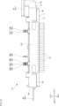
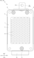
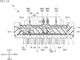
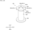
La présente invention concerne un dispositif à semi-conducteur qui comprend un substrat de support et au moins une borne. Le substrat de support a une surface principale dirigée vers un côté dans la direction de l'épaisseur. La ou les bornes sont disposées sur la surface principale, et comprennent un support électroconducteur, et une broche métallique qui est ajustée par pression dans la surface circonférentielle interne du support, la broche métallique faisant saillie plus loin vers un côté dans la direction de l'épaisseur que le support. Au moins une saillie qui fait saillie radialement vers l'intérieur est disposée sur la surface circonférentielle interne du support. La ou les saillies viennent en butée contre la surface circonférentielle externe de la broche métallique.
Applications Claiming Priority (2)
| Application Number | Priority Date | Filing Date | Title |
|---|---|---|---|
| JP2022118714 | 2022-07-26 | ||
| JP2022-118714 | 2022-07-26 |
Publications (1)
| Publication Number | Publication Date |
|---|---|
| WO2024024378A1 true WO2024024378A1 (fr) | 2024-02-01 |
Family
ID=89706064
Family Applications (1)
| Application Number | Title | Priority Date | Filing Date |
|---|---|---|---|
| PCT/JP2023/023922 WO2024024378A1 (fr) | 2022-07-26 | 2023-06-28 | Dispositif à semi-conducteur |
Country Status (1)
| Country | Link |
|---|---|
| WO (1) | WO2024024378A1 (fr) |
Citations (4)
| Publication number | Priority date | Publication date | Assignee | Title |
|---|---|---|---|---|
| US20090194884A1 (en) * | 2008-01-23 | 2009-08-06 | Infineon Technologies Ag | Power semiconductor module including a contact element |
| JP2010129670A (ja) * | 2008-11-26 | 2010-06-10 | Mitsubishi Electric Corp | 電力用半導体モジュール |
| WO2014069406A1 (fr) * | 2012-10-29 | 2014-05-08 | 富士電機株式会社 | Dispositif semi-conducteur |
| JP2021190221A (ja) * | 2020-05-27 | 2021-12-13 | 富士電機株式会社 | 半導体装置 |
-
2023
- 2023-06-28 WO PCT/JP2023/023922 patent/WO2024024378A1/fr unknown
Patent Citations (4)
| Publication number | Priority date | Publication date | Assignee | Title |
|---|---|---|---|---|
| US20090194884A1 (en) * | 2008-01-23 | 2009-08-06 | Infineon Technologies Ag | Power semiconductor module including a contact element |
| JP2010129670A (ja) * | 2008-11-26 | 2010-06-10 | Mitsubishi Electric Corp | 電力用半導体モジュール |
| WO2014069406A1 (fr) * | 2012-10-29 | 2014-05-08 | 富士電機株式会社 | Dispositif semi-conducteur |
| JP2021190221A (ja) * | 2020-05-27 | 2021-12-13 | 富士電機株式会社 | 半導体装置 |
Similar Documents
| Publication | Publication Date | Title |
|---|---|---|
| US8680666B2 (en) | Bond wireless power module with double-sided single device cooling and immersion bath cooling | |
| KR100566046B1 (ko) | 파워 반도체장치 | |
| US8749977B2 (en) | Power semiconductor module and its attachment structure | |
| CN110137160B (zh) | 半导体器件 | |
| CN108735692B (zh) | 半导体装置 | |
| US20120235293A1 (en) | Semiconductor device including a base plate | |
| US20110292611A1 (en) | Semiconductor-device cooling structure and power converter | |
| CN114175234A (zh) | 半导体装置及电子装置 | |
| JP2000323593A (ja) | 半導体装置 | |
| CN116259594A (zh) | 半导体装置及半导体装置的制造方法 | |
| JP2001036002A (ja) | 半導体装置 | |
| WO2024024378A1 (fr) | Dispositif à semi-conducteur | |
| WO2022080072A1 (fr) | Module semi-conducteur | |
| WO2024029274A1 (fr) | Dispositif à semi-conducteur | |
| JP7392319B2 (ja) | 半導体装置 | |
| WO2024024372A1 (fr) | Dispositif à semi-conducteur, unité de conversion de puissance électrique et procédé de fabrication de dispositif à semi-conducteur | |
| WO2023190180A1 (fr) | Dispositif à semi-conducteur | |
| WO2023214500A1 (fr) | Dispositif à semi-conducteur | |
| WO2023189840A1 (fr) | Dispositif à semi-conducteur | |
| WO2023140050A1 (fr) | Dispositif à semi-conducteur | |
| WO2023017708A1 (fr) | Dispositif à semi-conducteurs | |
| WO2024057860A1 (fr) | Dispositif à semi-conducteur | |
| WO2023243464A1 (fr) | Dispositif à semi-conducteur, module à semi-conducteur et structure de montage de module à semi-conducteur | |
| WO2022264834A1 (fr) | Dispositif à semi-conducteurs | |
| WO2024070581A1 (fr) | Unité de conversion de puissance électrique |
Legal Events
| Date | Code | Title | Description |
|---|---|---|---|
| 121 | Ep: the epo has been informed by wipo that ep was designated in this application |
Ref document number: 23846111 Country of ref document: EP Kind code of ref document: A1 |