WO2024075589A1 - Dispositif à semi-conducteur - Google Patents
Dispositif à semi-conducteur Download PDFInfo
- Publication number
- WO2024075589A1 WO2024075589A1 PCT/JP2023/034861 JP2023034861W WO2024075589A1 WO 2024075589 A1 WO2024075589 A1 WO 2024075589A1 JP 2023034861 W JP2023034861 W JP 2023034861W WO 2024075589 A1 WO2024075589 A1 WO 2024075589A1
- Authority
- WO
- WIPO (PCT)
- Prior art keywords
- conductive member
- metal layer
- insulating spacer
- semiconductor device
- connection members
- Prior art date
Links
- 239000004065 semiconductor Substances 0.000 title claims abstract description 220
- 125000006850 spacer group Chemical group 0.000 claims abstract description 146
- 229910052751 metal Inorganic materials 0.000 claims abstract description 138
- 239000002184 metal Substances 0.000 claims abstract description 138
- 229920005989 resin Polymers 0.000 claims abstract description 72
- 239000011347 resin Substances 0.000 claims abstract description 72
- 238000007789 sealing Methods 0.000 claims abstract description 59
- 230000003068 static effect Effects 0.000 claims description 29
- 230000009477 glass transition Effects 0.000 claims description 16
- 238000001514 detection method Methods 0.000 description 54
- 239000010949 copper Substances 0.000 description 43
- 239000000463 material Substances 0.000 description 28
- RYGMFSIKBFXOCR-UHFFFAOYSA-N Copper Chemical compound [Cu] RYGMFSIKBFXOCR-UHFFFAOYSA-N 0.000 description 23
- 229910052802 copper Inorganic materials 0.000 description 23
- 239000000203 mixture Substances 0.000 description 13
- 230000017525 heat dissipation Effects 0.000 description 9
- 230000004048 modification Effects 0.000 description 9
- 238000012986 modification Methods 0.000 description 9
- 239000010931 gold Substances 0.000 description 8
- 238000000034 method Methods 0.000 description 7
- 239000000758 substrate Substances 0.000 description 6
- 239000004020 conductor Substances 0.000 description 5
- 230000005669 field effect Effects 0.000 description 5
- 238000004519 manufacturing process Methods 0.000 description 5
- 229910000679 solder Inorganic materials 0.000 description 5
- 150000001875 compounds Chemical class 0.000 description 4
- 239000003822 epoxy resin Substances 0.000 description 4
- PCHJSUWPFVWCPO-UHFFFAOYSA-N gold Chemical compound [Au] PCHJSUWPFVWCPO-UHFFFAOYSA-N 0.000 description 4
- 229910052737 gold Inorganic materials 0.000 description 4
- 229920000647 polyepoxide Polymers 0.000 description 4
- 230000015572 biosynthetic process Effects 0.000 description 3
- 239000011162 core material Substances 0.000 description 3
- 239000011810 insulating material Substances 0.000 description 3
- 239000007769 metal material Substances 0.000 description 3
- 229920002050 silicone resin Polymers 0.000 description 3
- 238000005304 joining Methods 0.000 description 2
- HBMJWWWQQXIZIP-UHFFFAOYSA-N silicon carbide Chemical compound [Si+]#[C-] HBMJWWWQQXIZIP-UHFFFAOYSA-N 0.000 description 2
- 229910052709 silver Inorganic materials 0.000 description 2
- 239000004332 silver Substances 0.000 description 2
- 238000003466 welding Methods 0.000 description 2
- PIGFYZPCRLYGLF-UHFFFAOYSA-N Aluminum nitride Chemical compound [Al]#N PIGFYZPCRLYGLF-UHFFFAOYSA-N 0.000 description 1
- 229910000881 Cu alloy Inorganic materials 0.000 description 1
- 229910045601 alloy Inorganic materials 0.000 description 1
- 239000000956 alloy Substances 0.000 description 1
- 229910052782 aluminium Inorganic materials 0.000 description 1
- XAGFODPZIPBFFR-UHFFFAOYSA-N aluminium Chemical compound [Al] XAGFODPZIPBFFR-UHFFFAOYSA-N 0.000 description 1
- 238000005219 brazing Methods 0.000 description 1
- 239000000919 ceramic Substances 0.000 description 1
- 238000006243 chemical reaction Methods 0.000 description 1
- 238000010292 electrical insulation Methods 0.000 description 1
- 230000002349 favourable effect Effects 0.000 description 1
- 238000010438 heat treatment Methods 0.000 description 1
- 230000006872 improvement Effects 0.000 description 1
- 230000008595 infiltration Effects 0.000 description 1
- 238000001764 infiltration Methods 0.000 description 1
- 230000002452 interceptive effect Effects 0.000 description 1
- 230000001678 irradiating effect Effects 0.000 description 1
- 239000007788 liquid Substances 0.000 description 1
- 238000000465 moulding Methods 0.000 description 1
- 230000008569 process Effects 0.000 description 1
Images


Classifications
-
- H—ELECTRICITY
- H01—ELECTRIC ELEMENTS
- H01L—SEMICONDUCTOR DEVICES NOT COVERED BY CLASS H10
- H01L23/00—Details of semiconductor or other solid state devices
- H01L23/48—Arrangements for conducting electric current to or from the solid state body in operation, e.g. leads, terminal arrangements ; Selection of materials therefor
-
- H—ELECTRICITY
- H01—ELECTRIC ELEMENTS
- H01L—SEMICONDUCTOR DEVICES NOT COVERED BY CLASS H10
- H01L25/00—Assemblies consisting of a plurality of individual semiconductor or other solid state devices ; Multistep manufacturing processes thereof
- H01L25/03—Assemblies consisting of a plurality of individual semiconductor or other solid state devices ; Multistep manufacturing processes thereof all the devices being of a type provided for in the same subgroup of groups H01L27/00 - H01L33/00, or in a single subclass of H10K, H10N, e.g. assemblies of rectifier diodes
- H01L25/04—Assemblies consisting of a plurality of individual semiconductor or other solid state devices ; Multistep manufacturing processes thereof all the devices being of a type provided for in the same subgroup of groups H01L27/00 - H01L33/00, or in a single subclass of H10K, H10N, e.g. assemblies of rectifier diodes the devices not having separate containers
- H01L25/07—Assemblies consisting of a plurality of individual semiconductor or other solid state devices ; Multistep manufacturing processes thereof all the devices being of a type provided for in the same subgroup of groups H01L27/00 - H01L33/00, or in a single subclass of H10K, H10N, e.g. assemblies of rectifier diodes the devices not having separate containers the devices being of a type provided for in group H01L29/00
-
- H—ELECTRICITY
- H01—ELECTRIC ELEMENTS
- H01L—SEMICONDUCTOR DEVICES NOT COVERED BY CLASS H10
- H01L25/00—Assemblies consisting of a plurality of individual semiconductor or other solid state devices ; Multistep manufacturing processes thereof
- H01L25/18—Assemblies consisting of a plurality of individual semiconductor or other solid state devices ; Multistep manufacturing processes thereof the devices being of types provided for in two or more different subgroups of the same main group of groups H01L27/00 - H01L33/00, or in a single subclass of H10K, H10N
Definitions
- This disclosure relates to a semiconductor device.
- Patent Document 1 discloses an example of a conventional semiconductor device.
- the semiconductor device disclosed in this document comprises multiple semiconductor elements, multiple conductive members, and multiple wires.
- the semiconductor elements and the conductive members are electrically connected by wires.
- the conductive material When bonding a wire to a conductive material, the conductive material may bend, making it difficult to achieve a stable conductive connection.
- One of the objectives of this disclosure is to provide a semiconductor device that is an improvement over conventional semiconductor devices.
- one of the objectives of this disclosure is to provide a semiconductor device that is capable of more stable conductive connection.
- a semiconductor device provided by one aspect of the present disclosure includes a metal layer, a semiconductor element, a conductive member, a connection member, an insulating spacer, and a sealing resin.
- the semiconductor element is mounted on the metal layer.
- the conductive member is spaced from the metal layer in the thickness direction of the metal layer.
- the snow statue member electrically connects the semiconductor element and the conductive member.
- the sealing resin covers at least a portion of each of the metal layer, the semiconductor element, the conductive member, and the connection member.
- the insulating spacer is interposed between the metal layer and the conductive member.
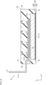
- FIG. 1 is a plan view showing a semiconductor device according to a first embodiment of the present disclosure.
- FIG. 2 is a bottom view showing the semiconductor device according to the first embodiment of the present disclosure.
- FIG. 3 is a side view showing the semiconductor device according to the first embodiment of the present disclosure.
- FIG. 4 is a cross-sectional view taken along line IV-IV in FIG.
- FIG. 5 is a cross-sectional view taken along line VV in FIG.
- FIG. 6 is a cross-sectional view taken along line VI-VI in FIG.
- FIG. 7 is a cross-sectional view taken along line VII-VII in FIG.
- FIG. 8 is a cross-sectional view taken along line VIII-VIII in FIG.
- FIG. 9 is a cross-sectional view taken along line IX-IX of FIG.
- FIG. 10 is a cross-sectional view taken along line XX in FIG.
- FIG. 11 is a cross-sectional view taken along line XI-XI of FIG.
- FIG. 12 is a cross-sectional view showing a first modified example of the semiconductor device according to the first embodiment of the present disclosure.
- FIG. 13 is a cross-sectional view showing a second modification of the semiconductor device according to the first embodiment of the present disclosure.
- FIG. 14 is a cross-sectional view showing a third modified example of the semiconductor device according to the first embodiment of the present disclosure.
- FIG. 15 is a plan view showing a semiconductor device according to the second embodiment of the present disclosure.
- FIG. 16 is a cross-sectional view taken along line XVI-XVI in FIG.
- FIG. 17 is a cross-sectional view taken along line XVII-XVII in FIG.
- an object A is formed on an object B" and “an object A is formed on an object B” include “an object A is formed directly on an object B” and “an object A is formed on an object B with another object interposed between the object A and the object B” unless otherwise specified.
- an object A is disposed on an object B” and “an object A is disposed on an object B” include “an object A is disposed directly on an object B” and “an object A is disposed on an object B with another object interposed between the object A and the object B" unless otherwise specified.
- an object A is located on an object B includes “an object A is located on an object B in contact with an object B” and “an object A is located on an object B with another object interposed between the object A and the object B” unless otherwise specified.
- an object A overlaps an object B when viewed in a certain direction includes “an object A overlaps the entire object B” and “an object A overlaps a part of an object B.”
- a surface A faces in direction B is not limited to the case where the angle of surface A with respect to direction B is 90°, but also includes the case where surface A is tilted with respect to direction B.
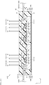
- First embodiment: 1 to 11 show a semiconductor device according to the first embodiment of the present disclosure.
- the semiconductor device A10 of this embodiment includes a conductive member 11, a conductive member 12, a first conductive member 13, a plurality of first connection members 14, a plurality of second connection members 15, a plurality of first semiconductor elements 21, a plurality of second semiconductor elements 22, and a sealing resin 50.
- the semiconductor device A10 includes a second conductive member 171, a third conductive member 172, a fourth conductive member 181, a fifth conductive member 182, a plurality of dummy terminals 19, a plurality of third connection members 41, a plurality of fifth connection members 42, a plurality of fourth connection members 43, and a plurality of sixth connection members 44.
- the semiconductor device A10 includes a first insulating spacer 61, a second insulating spacer 62, and a third insulating spacer 63.
- the semiconductor device A10 converts a DC power supply voltage applied to a first terminal 112 and a third terminal 132 (described later) into AC power by a plurality of first semiconductor elements 21 and a plurality of second semiconductor elements 22.
- the converted AC power is input to a power supply target such as a motor from a second terminal 122 described later.
- the semiconductor device A10 constitutes a part of a power conversion circuit such as an inverter. Note that the use and specific configuration of the semiconductor device according to the present invention are not limited in any way.
- FIG. 1 is a plan view of the semiconductor device A10.
- FIG. 2 is a bottom view of the semiconductor device A10.
- FIG. 3 is a side view of the semiconductor device A10.
- FIG. 4 is a cross-sectional view taken along line IV-IV in FIG. 1.
- FIG. 5 is a cross-sectional view taken along line V-V in FIG. 1.
- FIG. 6 is a cross-sectional view taken along line VI-VI in FIG. 1.
- FIG. 7 is a cross-sectional view taken along line VII-VII in FIG. 1.
- FIG. 8 is a cross-sectional view taken along line VIII-VIII in FIG. 1.
- FIG. 9 is a cross-sectional view taken along line IX-IX in FIG. 1.
- FIG. 10 is a cross-sectional view taken along line X-X in FIG. 1.
- FIG. 11 is a cross-sectional view taken along line XI-XI in FIG. 1.
- the z direction is, for example, an example of the thickness
- the conductive member 11 includes a first metal layer 111, a first terminal 112, and a first dunnage material 113.
- the first metal layer 111 is a conductive material, and includes, for example, Cu (copper).
- the first metal layer 111 is located on one side in the x-direction of the semiconductor device A10.
- the first metal layer 111 has a first main surface 111A.
- the first main surface 111A faces one side in the z-direction. In the illustrated example, the first main surface 111A is a flat surface.
- the first terminal 112 protrudes to one side in the x direction and has a portion exposed from the sealing resin 50.
- the first terminal 112 protrudes to one side in the x direction from the sealing resin 50 and has a portion exposed.
- the first terminal 112 is located on one side in the x direction of the first metal layer 111.
- the first terminal 112 is located on the other side in the y direction of the first metal layer 111.
- a portion of the first terminal 112 on the other side in the x direction overlaps with a portion of the first metal layer 111 on the other side in the y direction in the z direction.
- the first terminal 112 is located on one side in the z direction with respect to the first main surface 111A and is separated from the first metal layer 111.
- the first terminal 112 has a first mounting hole 112A. The first mounting hole 112A penetrates the first terminal 112 in the z direction.
- the first dunnage material 113 is interposed between the first metal layer 111 and the first terminal 112.
- the composition of the first dunnage material 113 includes Cu (copper).
- the first dunnage material 113 is conductively joined to the first main surface 111A of the first metal layer 111 and the first terminal 112. There are no limitations on the method of conductive joining, and a method using a conductive bonding material such as solder, a method such as welding, etc. may be appropriately adopted.
- the first metal layer 111 is supported by a support member 10A.
- the support member 10A is located on the opposite side of the first metal layer 111 from the first main surface 111A.
- the support member 10A is composed of a DBC (Direct Bonded Copper) substrate, an AMB (Active Metal Brazing) substrate, or the like.
- the support member 10A includes an insulating layer 101, a support layer 102, and a heat dissipation layer 103.
- the support member 10A is covered with a sealing resin 50 except for a portion of the heat dissipation layer 103.
- the insulating layer 101 includes a portion located between the support layer 102 and the heat dissipation layer 103 in the z direction.
- the insulating layer 101 may be a material with high thermal conductivity.
- the insulating layer 101 may be, for example, a ceramic including an aluminum nitride (AlN) sintered body. The thickness of the insulating layer 101 is thinner than the thickness of the first metal layer 111.
- the support layer 102 is located between the insulating layer 101 and the first metal layer 111 in the z direction.
- the composition of the support layer 102 includes copper (Cu).
- Cu copper
- the outer periphery of the support layer 102 is located inside the outer periphery of the insulating layer 101.
- the support layer 102 is bonded to the first metal layer 111.
- the support layer 102 and the first metal layer 111 are bonded, for example, via solder.
- the heat dissipation layer 103 is located on the opposite side of the insulating layer 101 from the support layer 102 in the z direction. A part of the heat dissipation layer 103 is exposed from the sealing resin 50.
- a heat sink (not shown) is joined to the heat dissipation layer 103.
- the composition of the heat dissipation layer 103 includes copper. When viewed in the z direction, the outer periphery of the heat dissipation layer 103 is located inside the outer periphery of the insulating layer 101.
- the conductive member 12 includes a second metal layer 121, a second terminal 122, and a second dunnage material 123.
- the second metal layer 121 is a conductive material, and includes, for example, Cu (copper).
- the second metal layer 121 is located on the other side of the semiconductor device A10 in the x direction.
- the second metal layer 121 has a second main surface 121A.
- the second main surface 121A faces one side in the z direction. In the illustrated example, the second main surface 121A is a flat surface.
- the second terminal 122 protrudes to the other side in the x direction and has a portion exposed from the sealing resin 50.
- the second terminal 122 protrudes to the other side in the x direction from the sealing resin 50 and has an exposed portion.
- the second terminal 122 is located on the other side in the x direction of the second metal layer 121.
- a portion of one side of the first terminal 112 in the x direction overlaps in the z direction with a portion of the other side in the x direction of the second metal layer 121.
- the center position of the second terminal 122 in the y direction approximately coincides with the center position of the second metal layer 121 in the y direction.
- the second terminal 122 is located on one side in the z direction with respect to the second main surface 121A and is separated from the second metal layer 121. A portion of one side of the second terminal 122 in the x direction overlaps with the center of the second main surface 121A in the y direction when viewed in the z direction.
- the composition of the second terminal 122 includes Cu (copper).
- the second terminal 122 has a second mounting hole 122A. The second mounting hole 122A penetrates the second terminal 122 in the z direction.
- the second dunnage material 123 is interposed between the second metal layer 121 and the second terminal 122, as shown in FIG. 1 and FIG. 4 to FIG. 6.
- the composition of the second dunnage material 123 includes Cu (copper).
- the second dunnage material 123 is conductively joined to the second main surface 121A of the second metal layer 121 and the second terminal 122. There are no limitations on the method of conductive joining, and a method using a conductive joining material such as solder, a method such as welding, etc. may be appropriately adopted.
- the second metal layer 121 is supported by a support member 10B.
- the support member 10B is located on the opposite side of the second metal layer 121 from the second main surface 121A.
- First semiconductor element 21 As shown in FIG. 1 and FIG. 4 to FIG. 7, the first semiconductor elements 21 are bonded to the first main surface 111A of the first metal layer 111.
- the first semiconductor elements 21 are all identical elements.
- Each of the first semiconductor elements 21 may be, for example, a field effect transistor including a metal-oxide-semiconductor field-effect transistor (MOSFET) or a metal-insulator-semiconductor field-effect transistor (MISFET), or a bipolar transistor such as an insulated gate bipolar transistor (IGBT).
- MOSFET metal-oxide-semiconductor field-effect transistor
- MISFET metal-insulator-semiconductor field-effect transistor
- IGBT insulated gate bipolar transistor
- each of the first semiconductor elements 21 may be a diode.
- the first semiconductor elements 21 are n-channel type MOSFETs having a vertical structure.
- the first semiconductor elements 21 include a compound semiconductor substrate.
- the composition of the compound semiconductor substrate includes
- Each of the first semiconductor elements 21 has a first drain electrode 211, a first source electrode 212, and a first gate electrode 213.
- the first drain electrode 211 is located on the other side in the z direction of the first semiconductor element 21.
- the first drain electrode 211 faces the first main surface 111A of the first metal layer 111.
- the first drain electrode 211 is configured to allow a current corresponding to the power before being converted by the first semiconductor element 21 to flow through it.
- the first drain electrode 211 is conductively bonded to the first main surface 111A via a conductive bonding layer 29.
- Each of the first drain electrodes 211 of the multiple first semiconductor elements 21 is conductive to the conductive member 11.
- the conductive bonding layer 29 can be, for example, either solder or a sintered metal including silver or the like.
- the first source electrode 212 is located on one side of the first semiconductor element 21 in the z direction.
- the first source electrode 212 is located on the opposite side of the first drain electrode 211 in the z direction.
- the first source electrode 212 is configured to allow a current corresponding to the power converted by the first semiconductor element 21 to flow through it.
- the first gate electrode 213 is located on one side of the first semiconductor element 21 in the z direction.
- the first gate electrode 213 is located on the same side of the first semiconductor element 21 as the first source electrode 212 in the z direction.
- the first gate electrode 213 is configured to receive a gate voltage for driving the first semiconductor element 21. As shown in FIG. 3, the area of the first gate electrode 213 is smaller than the area of the first source electrode 212 when viewed in the z direction.
- Second semiconductor element 22 The second semiconductor elements 22 are bonded to the second main surface 121A of the second metal layer 121 as shown in FIG. 1 and FIG. 4 to FIG. 6.
- the second semiconductor elements 22 are the same elements as the first semiconductor elements 21.
- Each of the second semiconductor elements 22 may be an n-channel type MOSFET having a vertical structure.
- Each of the second semiconductor elements 22 may be either a field effect transistor including a metal-insulator-semiconductor field-effect transistor (MISFET) or a bipolar transistor such as an insulated gate bipolar transistor (IGBT).
- MISFET metal-insulator-semiconductor field-effect transistor
- IGBT insulated gate bipolar transistor
- Each of the second semiconductor elements 22 may be a diode.
- the second semiconductor elements 22 are n-channel type MOSFETs having a vertical structure.
- the second semiconductor elements 22 include a compound semiconductor substrate.
- the composition of the compound semiconductor substrate includes silicon carbide (SiC).
- Each of the multiple second semiconductor elements 22 has a second drain electrode 221, a second source electrode 222, and a second gate electrode 223.
- the second drain electrode 221 is located on one side in the z direction in the second semiconductor element 22.
- the second gate electrode 223 faces the second main surface 121A of the second metal layer 121 in the second semiconductor element 22.
- the second drain electrode 221 is configured so that a current corresponding to the power before being converted by the second semiconductor element 22 flows through it.
- the second drain electrode 221 is conductively bonded to the second main surface 121A via the conductive bonding layer 29.
- Each of the second drain electrodes 221 of the multiple second semiconductor elements 22 is electrically connected to the conductive member 12.
- the second source electrode 222 is located on one side of the second semiconductor element 22 in the z direction.
- the second source electrode 222 is located on the opposite side of the second drain electrode 221 in the z direction of the second semiconductor element 22.
- the second source electrode 222 is configured to allow a current corresponding to the power converted by the second semiconductor element 22 to flow through it.
- the second gate electrode 223 is located on one side of the second semiconductor element 22 in the z direction.
- the second source electrode 222 is located on the same side of the second semiconductor element 22 as the second source electrode 222 in the z direction.
- the second gate electrode 223 is configured to receive a gate voltage for driving the second semiconductor element 22. When viewed in the z direction, the area of the second gate electrode 223 is smaller than the area of the second source electrode 222.
- First conductive member 13 1, 2, and 4 to 7, the first conductive member 13 includes an extension 131 and a third terminal 132.
- the first conductive member 13 is a conductive material and includes, for example, Cu (copper).
- the third terminal 132 has a portion protruding from the sealing resin 50 to one side in the x direction.
- the third terminal 132 has a portion protruding from the sealing resin 50 to one side in the x direction and exposed.
- the third terminal 132 is located on one side in the y direction with respect to the first terminal 112.
- the third terminal 132 is located on one side in the x direction of the first metal layer 111.
- the third terminal 132 is located on one side in the z direction with respect to the first main surface 111A and is separated from the first metal layer 111.
- a portion of the other side in the x direction of the third terminal 132 overlaps a portion of the one side in the x direction of the first main surface 111A when viewed in the z direction.
- the composition of the third terminal 132 includes Cu (copper).
- the third terminal 132 has a third mounting hole 132A.
- the third mounting hole 132A penetrates the third terminal 132 in the z direction.
- the extension portion 131 extends from the third terminal 132 to the other side in the x-direction.
- the extension portion 131 is covered with the sealing resin 50.
- the extension portion 131 includes a first portion 1311, a second portion 1312, and a third portion 1313.
- the distance z1 of the first portion 1311 from the first main surface 111A in the z direction is smaller than the distance z0 from the first main surface 111A to the third terminal 132 in the z direction.
- the magnitude of the distance z1 is, for example, 0.1 mm or more.
- the first portion 1311 is located between the multiple first semiconductor elements 21 and the multiple second semiconductor elements 22 in the x direction.
- the distance z1 is larger than the distance z2 from the first main surface 111A in the z direction to one side end of the first semiconductor element 21 in the z direction.
- the distance z2 is about 0.5 mm
- the distance z1 is about 0.8 mm to 1.2 mm.
- the shape of the first portion 1311 is not limited in any way, and in this embodiment, it is a shape that extends in the y direction.
- the first portion 1311 is, for example, a flat band shape.
- the first portion 1311 overlaps with the first main surface 111A (first metal layer 111) when viewed in the z direction.
- the other end edge of the first portion 1311 in the x direction is located on one side in the x direction of the other end edge of the first main surface 111A in the x direction.
- the second portion 1312 is connected to the third terminal 132.
- the second portion 1312 extends from the third terminal 132 along the x direction to the other side in the x direction.
- the shape of the second portion 1312 is not limited in any way, and may be, for example, a flat band.
- the distance in the z direction from the first main surface 111A to the second portion 1312 is the same as (or approximately the same as) the distance z0.
- the second portion 1312 is located on one side in the y direction (the right side in FIG. 1) with respect to the multiple first semiconductor elements 21.
- the other edge in the x direction of the second portion 1312 is located on the other side in the x direction of the one edge in the x direction of the first semiconductor element 21.
- the third portion 1313 is interposed between the first portion 1311 and the second portion 1312.
- the extension portion 131 has a bent shape when viewed in the y direction.
- the third portion 1313 is part of one side edge of the first portion 1311 in the x direction, and is connected to a portion closer to one side end in the y direction.
- the third portion 1313 is connected to a portion of the second portion 1312 on the other side in the x direction.
- First connecting member 14 As shown in FIG. 1, FIG. 5, and FIG. 7, the first connection members 14 individually conduct the first semiconductor elements 21 and the conductive member 12. More specifically, the first connection members 14 are connected to the first source electrode 212 of the first semiconductor element 21 and the second main surface 121A of the second metal layer 121.
- the specific configuration of the first connection members 14 is not limited, and may be, for example, a wire or ribbon containing a metal material.
- the metal material may include, for example, Cu (copper), Al (aluminum), or an alloy thereof.
- the first connection members 14 in this example are wires containing Cu (copper).
- the number of the first connection members 14 is not limited, and in the illustrated example, two first connection members 14 are connected to the first source electrode 212 of one first semiconductor element 21 and the first main surface 111A of the first metal layer 111.
- the first connecting member 14 straddles the first portion 1311 to one side in the z direction. That is, the first connecting member 14 has a portion that is separated from the first portion 1311 to one side in the z direction. In the illustrated example, the first connecting member 14 has a curved shape that straddles the first portion 1311 to one side in the z direction.
- Second connecting member 15 As shown in FIGS. 1, 4, 6 and 7, the second connection members 15 individually conduct the second semiconductor elements 22 and the first conductive member 13. More specifically, the second connection members 15 are connected to the second source electrode 222 of the second semiconductor element 22 and the first portion 1311 of the extension portion 131 of the first conductive member 13.
- the specific configuration of the second connection members 15 is not limited in any way, and may be, for example, a wire and ribbon containing a metal material, or a plate material.
- the second connection members 15 may be separate from the first conductive member 13, or may be integrated with the first conductive member 13. In this embodiment, the second connection members 15 are separate from the first conductive member 13 and are, for example, wires containing Cu (copper).
- the number of second connection members 15 is not limited in any way, and in the example shown, two second connection members 15 are connected to the second source electrode 222 of one second semiconductor element 22 and the second main surface 121A of the second metal layer 121.
- the multiple first connection members 14 and the multiple second connection members 15 are aligned in the y direction.
- two first connection members 14 and two second connection members 15 are aligned alternately in the y direction.
- the second conductive member 171 includes a first gate terminal 1711, a first gate wiring portion 1712, and a step portion 1713.
- the second conductive member 171 is a so-called lead member, and contains, for example, Cu (copper) in its composition.
- the first gate terminal 1711 is located outside the sealing resin 50, and functions as a gate terminal capable of supplying a gate voltage to the multiple first semiconductor elements 21 of the semiconductor device A10.
- the first gate wiring portion 1712 is located on one side in the x direction with respect to the multiple first semiconductor elements 21.
- the first gate wiring portion 1712 is separated from the first main surface 111A of the first metal layer 111 on one side in the z direction.
- the first gate wiring portion 1712 has a shape extending in the y direction. The distance from the first main surface 111A to the first gate wiring portion 1712 in the z direction is smaller than the distance from the first main surface 111A to the first gate terminal 1711 in the z direction.
- the first gate wiring portion 1712 is individually conductively connected to each of the first gate electrodes 213 of the multiple first semiconductor elements 21 by multiple third connection members 41.
- the third connection members 41 may be wires containing, for example, Au (gold), Cu (copper), or the like.
- the step portion 1713 is located between the first gate terminal 1711 and the first gate wiring portion 1712. By having the step portion 1713, the second conductive member 171 may have a bent shape when viewed in the x-direction.
- the fourth conductive member 181 includes a first detection terminal 1811, a first detection wiring portion 1812, and a step portion 1813, as shown in Figures 1 to 6 and 8.
- the fourth conductive member 181 is a so-called lead member, and contains, for example, Cu (copper) in its composition.
- the first detection terminal 1811 is located outside the sealing resin 50, and functions as a detection terminal capable of detecting the operating state of the multiple first semiconductor elements 21 of the semiconductor device A10.
- the first detection wiring portion 1812 is located on one side in the x direction with respect to the first gate wiring portion 1712.
- the first detection wiring portion 1812 is separated from the first main surface 111A of the first metal layer 111 on one side in the z direction.
- the first detection wiring portion 1812 has a shape extending in the y direction. The distance from the first main surface 111A to the first detection wiring portion 1812 in the z direction is smaller than the distance from the first main surface 111A to the first detection terminal 1811 in the z direction.
- the first detection wiring portion 1812 is individually conductively connected to each of the first source electrodes 212 of the first semiconductor elements 21 by a plurality of fifth connection members 42.
- the fifth connection members 42 may be wires containing, for example, Au (gold), Cu (copper), or the like.
- the step portion 1813 is located between the first detection terminal 1811 and the first detection wiring portion 1812. By having the step portion 1813, the fourth conductive member 181 may have a bent shape when viewed in the x direction.
- the third conductive member 172 includes a second gate terminal 1721, a second gate wiring portion 1722, and a step portion 1723.
- the third conductive member 172 is a so-called lead member, and contains, for example, Cu (copper) in its composition.
- the second gate terminal 1721 is located outside the sealing resin 50, and functions as a gate terminal capable of supplying a gate voltage to the plurality of second semiconductor elements 22 of the semiconductor device A10.
- the second gate wiring portion 1722 is located on the other side in the x direction with respect to the plurality of second semiconductor elements 22.
- the second gate wiring portion 1722 is spaced apart from the first main surface 111A of the first metal layer 111 on one side in the z direction.
- the second gate wiring portion 1722 has a shape extending in the y direction. The distance from the first main surface 111A to the second gate wiring portion 1722 in the z direction is smaller than the distance from the first main surface 111A to the second gate terminal 1721 in the z direction.
- the second gate wiring portion 1722 is individually conductively connected to each of the second gate electrodes 223 of the second semiconductor elements 22 by a plurality of fourth connection members 43.
- the fourth connection members 43 may be wires containing, for example, Au (gold), Cu (copper), or the like.
- the step portion 1723 is located between the second gate terminal 1721 and the second gate wiring portion 1722. By having the step portion 1723, the third conductive member 172 may have a bent shape when viewed in the x-direction.
- the fifth conductive member 182 includes a second detection terminal 1821, a second detection wiring portion 1822, and a step portion 1823, as shown in Figures 1 to 6 and 11.
- the fifth conductive member 182 is a so-called lead member, and contains, for example, Cu (copper) in its composition.
- the second detection terminal 1821 is located outside the sealing resin 50, and functions as a detection terminal capable of detecting the operating state of the multiple second semiconductor elements 22 of the semiconductor device A10.
- the second detection wiring portion 1822 is located on the other side in the x direction relative to the second gate wiring portion 1722.
- the second detection wiring portion 1822 is separated from the first main surface 111A of the first metal layer 111 to one side in the z direction.
- the second detection wiring portion 1822 has a shape extending in the y direction. The distance from the first main surface 111A to the second detection wiring portion 1822 in the z direction is smaller than the distance from the first main surface 111A to the second detection terminal 1821 in the z direction.
- the second detection wiring portion 1822 is individually conductively connected to the second source electrodes 222 of the second semiconductor elements 22 by a plurality of sixth connection members 44.
- the sixth connection members 44 may be wires containing, for example, Au (gold), Cu (copper), or the like.
- the step portion 1823 is located between the second detection terminal 1821 and the second detection wiring portion 1822. By having the step portion 1823, the fifth conductive member 182 may have a bent shape when viewed in the x direction.
- the semiconductor device A10 further includes four dummy terminals 19, as shown in FIGS. 1 to 7. Two of the four dummy terminals 19 are located on both sides of the first gate terminal 1711 and the first detection terminal 1811 in the x direction. The remaining two dummy terminals 19 are located on both sides of the second gate terminal 1721 and the second detection terminal 1821 in the x direction.
- the dummy terminals 19 may be metal leads.
- the dummy terminals 19 may be made of a material containing copper or a copper alloy. A portion of each of the multiple dummy terminals 19 is covered with a sealing resin. The portions of the multiple dummy terminals 19 that stand up in the z direction are exposed from the sealing resin 50.
- the sealing resin 50 covers the first metal layer 111, the second metal layer 121, the first connection members 14, the second connection members 15, the first semiconductor elements 21, and the second semiconductor elements 22. Furthermore, the sealing resin 50 covers a part of each of the first terminal 112, the second terminal 122, and the third terminal 132, the extension portion 131, the first gate wiring portion 1712, the first detection wiring portion 1812, the second gate wiring portion 1722, and the second detection wiring portion 1822.
- the sealing resin 50 has electrical insulation properties.
- the sealing resin 50 may be a material containing, for example, a black epoxy resin.
- the sealing resin 50 has a top surface 51, a bottom surface 52, a first side surface 53, a second side surface 54, a third side surface 56, and a fourth side surface 56.
- the top surface 51 faces one side in the z direction.
- the bottom surface 52 faces the other side in the z direction.
- the first side 53 is a surface facing one side in the x-direction. A portion of the first terminal 112 and a portion of the third terminal 132 protrude from the first side 53.
- the second side 54 is a surface facing the other side in the x-direction. A portion of the second terminal 122 protrudes from the second side 54.
- the third side surface 55 faces one side in the y direction.
- the fourth side surface 56 faces the other side in the y direction.
- the first gate terminal 1711, the first detection terminal 1811, the second gate terminal 1721, the second detection terminal 1821 and the multiple dummy terminals 19 protrude from the fourth side surface 56.
- First insulating spacer 61 As shown in FIG. 1 and FIG. 4 to FIG. 7, the first insulating spacer 61 is interposed between the first portion 1311 of the extension portion 131, which is a part of the first conductive member 13, and the first metal layer 111.
- the first insulating spacer 61 is an insulating material, and includes, for example, epoxy resin, silicone resin, etc.
- the first insulating spacer 61 may have a configuration in which an insulating layer is provided on the surface of a conductive core material.
- the static friction coefficient between the first insulating spacer 61 and the first metal layer 111 and the static friction coefficient between the first insulating spacer 61 and the first conductive member 13 are preferably larger than the static friction coefficient between the first metal layer 111 and the first conductive member 13.
- the glass transition point of the first insulating spacer 61 is preferably higher than the glass transition point of the sealing resin 50.
- the shape of the first insulating spacer 61 is not limited in any way, and in the illustrated example, it is a strip extending in the y direction.
- the size of the first insulating spacer 61 in the z direction is, for example, 100 ⁇ m or more and 5000 ⁇ m or less.
- the first insulating spacer 61 is in contact with the first main surface 111A of the first metal layer 111.
- the first insulating spacer 61 is in contact with the first portion 1311. Note that a configuration may be adopted in which a portion of the sealing resin 50 has entered between the first insulating spacer 61 and the first portion 1311.
- the portion of the multiple second connection members 15 connected to the first portion 1311 overlaps the first insulating spacer 61 when viewed in the z direction.
- Second insulating spacer 62 As shown in FIG. 1, FIG. 4 to FIG. 6, FIG. 8 and FIG. 9, the second insulating spacer 62 is interposed between the first metal layer 111 and the second conductive member 171. The second insulating spacer 62 is interposed between the first metal layer 111 and the fourth conductive member 181.
- the second insulating spacer 62 is an insulating material, and includes, for example, epoxy resin, silicone resin, etc.
- the second insulating spacer 62 may have a configuration in which an insulating layer is provided on the surface of a conductive core material.
- the static friction coefficient between the second insulating spacer 62 and the first metal layer 111, the static friction coefficient between the second insulating spacer 62 and the second conductive member 171, and the static friction coefficient between the second insulating spacer 62 and the fourth conductive member 181 are preferably larger than the static friction coefficient between the first metal layer 111 and the second conductive member 171, and the static friction coefficient between the first metal layer 111 and the fourth conductive member 181.
- the glass transition point of the second insulating spacer 62 is preferably higher than the glass transition point of the sealing resin 50.
- the shape of the second insulating spacer 62 is not limited in any way, and in the illustrated example, it is a strip extending in the y direction.
- the size of the second insulating spacer 62 in the z direction is, for example, 100 ⁇ m or more and 5000 ⁇ m or less.
- the second insulating spacer 62 is in contact with the first main surface 111A of the first metal layer 111.
- the second insulating spacer 62 is in contact with the second conductive member 171 and the fourth conductive member 181.
- a configuration may be adopted in which a portion of the sealing resin 50 penetrates between the second insulating spacer 62 and the second conductive member 171 and the fourth conductive member 181.
- the portions of the multiple third connection members 41 and the multiple fifth connection members 42 that are connected to the second conductive member 171 or the fourth conductive member 181 overlap the second insulating spacer 62 when viewed in the z direction.
- Third insulating spacer 63 As shown in FIG. 1, FIG. 4 to FIG. 6, FIG. 10 and FIG. 11, the third insulating spacer 63 is interposed between the second metal layer 121 and the third conductive member 172. The third insulating spacer 63 is interposed between the second metal layer 121 and the fifth conductive member 182.
- the third insulating spacer 63 is an insulating material, and includes, for example, epoxy resin, silicone resin, etc.
- the third insulating spacer 63 may have a configuration in which an insulating layer is provided on the surface of a conductive core material.
- the static friction coefficient between the third insulating spacer 63 and the second metal layer 121, the static friction coefficient between the third insulating spacer 63 and the third conductive member 172, and the static friction coefficient between the third insulating spacer 63 and the fifth conductive member 182 are preferably larger than the static friction coefficient between the second metal layer 121 and the third conductive member 172, and the static friction coefficient between the second metal layer 121 and the fifth conductive member 182.
- the glass transition point of the third insulating spacer 63 is preferably higher than the glass transition point of the sealing resin 50.
- the shape of the third insulating spacer 63 is not limited, and in the illustrated example, it is a strip extending in the y direction.
- the size of the second insulating spacer 62 in the z direction is, for example, 100 ⁇ m or more and 5000 ⁇ m or less.
- the third insulating spacer 63 is in contact with the second main surface 121A of the second metal layer 121.
- the third insulating spacer 63 is in contact with the third conductive member 172 and the fifth conductive member 182. Note that a configuration may be adopted in which a part of the sealing resin 50 penetrates between the third insulating spacer 63 and the third conductive member 172 and the fifth conductive member 182.
- the parts of the multiple fourth connection members 43 and the multiple sixth connection members 44 that are connected to the third conductive member 172 or the fifth conductive member 182 overlap the third insulating spacer 63 when viewed in the z direction.
- At least one of the first insulating spacer 61 and the second insulating spacer 62 can be placed on the first main surface 111A of the first metal layer 111, for example, after mounting a plurality of first semiconductor elements 21 on the first metal layer 111.
- the third insulating spacer 63 can be placed on the second main surface 121A of the second metal layer 121, after mounting a plurality of second semiconductor elements 22 on the second metal layer 121.
- the first portion 1311 of the extension portion 131 of the first conductive member 13 is arranged on the first insulating spacer 61.
- the second conductive member 171 and the fourth conductive member 181 are arranged on the second insulating spacer 62.
- the third conductive member 172 and the fifth conductive member 182 are arranged on the third insulating spacer 63.
- one of the multiple first connection members 14 is connected to each of the first source electrodes 212 of the multiple first semiconductor elements 21 and the second metal layer 121.
- One of the multiple second connection members 15 is connected to each of the second source electrodes 222 of the multiple second semiconductor elements 22 and the first portion 1311.
- the force applied to the first portion 1311 is received by the first insulating spacer 61.
- any of the multiple third connection members 41 is connected to each of the first gate electrodes 213 of the multiple first semiconductor elements 21 and the second conductive member 171.
- the force applied to the second conductive member 171 is received by the second insulating spacer 62.
- Any of the multiple fifth connection members 42 is connected to each of the first source electrodes 212 of the multiple first semiconductor elements 21 and the fourth conductive member 181.
- the multiple fifth connection members 42 are connected to the fourth conductive member 181
- the force applied to the second conductive member 171 and the fourth conductive member 181 is received by the second insulating spacer 62.
- any of the multiple fourth connection members 43 is connected to each of the multiple second gate electrodes 223 of the multiple second semiconductor elements 22 and the third conductive member 172.
- the force applied to the third conductive member 172 is received by the third insulating spacer 63.
- Any of the multiple sixth connection members 44 is connected to each of the multiple second source electrodes 222 of the multiple second semiconductor elements 22 and the fifth conductive member 182.
- the multiple sixth connection members 44 are connected to the fifth conductive member 182
- the force applied to the fifth conductive member 182 is received by the third insulating spacer 63.
- the sealing resin 50 is formed by a resin molding process.
- the liquid resin material for forming the sealing resin 50 is filled into the space that is to become the sealing resin 50.
- This filling may cause the resin material to enter, for example, between the first insulating spacer 61 and the first portion 1311.
- the resin material may enter between the second insulating spacer 62 and the second conductive member 171 and the fourth conductive member 181.
- the resin material may enter between the third insulating spacer 63 and the third conductive member 172 and the fifth conductive member 182.
- a part of the sealing resin 50 may be present between the first insulating spacer 61 and the first portion 1311, between the second insulating spacer 62 and the second conductive member 171 and the fourth conductive member 181, and between the third insulating spacer 63 and the third conductive member 172 and the fifth conductive member 182.
- a portion of the sealing resin 50 may not be present between the first insulating spacer 61 and the first portion 1311, between the second insulating spacer 62 and the second conductive member 171 and the fourth conductive member 181, and between the third insulating spacer 63 and the third conductive member 172 and the fifth conductive member 182.
- a first insulating spacer 61 is interposed between the first main surface 111A of the first metal layer 111 and the first portion 1311 of the extension portion 131 of the first conductive member 13.
- the first insulating spacer 61 is an insulating member, and therefore can reduce the electrical connection between the first metal layer 111 and the extension portion 131.
- the first insulating spacer 61 can withstand the force applied to the first portion 1311 when connecting the second connection member 15. Therefore, the second connection member 15 can be more stably electrically connected.
- the static friction coefficient between the first insulating spacer 61 and the first metal layer 111 and the static friction coefficient between the first insulating spacer 61 and the first conductive member 13 are greater than the static friction coefficient between the first metal layer 111 and the first conductive member 13. This allows the first conductive member 13 to be more stably held by the first insulating spacer 61 when the second connection member 15 is conductively connected. Since the glass transition point of the first insulating spacer 61 is higher than the glass transition point of the sealing resin 50, deformation of the first insulating spacer 61 during the formation of the sealing resin 50 can be reduced.
- a second insulating spacer 62 is interposed between the first main surface 111A of the first metal layer 111 and the first gate wiring portion 1712 of the second conductive member 171 and the first detection wiring portion 1812 of the fourth conductive member 181.
- the second insulating spacer 62 is an insulating member, and therefore can reduce the electrical connection between the first metal layer 111 and the second conductive member 171 and the fourth conductive member 181.
- the second insulating spacer 62 can withstand the force applied to the first gate wiring portion 1712 and the first detection wiring portion 1812 when connecting the multiple third connection members 41 and the multiple fifth connection members 42. Therefore, the multiple third connection members 41 and the multiple fifth connection members 42 can be more stably conductively connected.
- the static friction coefficient between the second insulating spacer 62 and the first metal layer 111 and between the second insulating spacer 62 and the second conductive member 171 and the fourth conductive member 181 is greater than the static friction coefficient between the first metal layer 111 and the second conductive member 171 and the fourth conductive member 181.
- a third insulating spacer 63 is interposed between the second main surface 121A of the second metal layer 121 and the second gate wiring portion 1722 of the third conductive member 172 and the second detection wiring portion 1822 of the fifth conductive member 182.
- the third insulating spacer 63 is an insulating member, and therefore can reduce the electrical connection between the second metal layer 121 and the third conductive member 172 and the fifth conductive member 182.
- the third insulating spacer 63 can withstand the force applied to the second gate wiring portion 1722 and the second detection wiring portion 1822 when connecting the multiple fourth connection members 43 and the multiple sixth connection members 44. Therefore, the multiple fourth connection members 43 and the multiple sixth connection members 44 can be more stably conductively connected.
- the static friction coefficient between the third insulating spacer 63 and the second metal layer 121, the static friction coefficient between the third insulating spacer 63 and the third conductive member 172, and the static friction coefficient between the third insulating spacer 63 and the fifth conductive member 182 are greater than the static friction coefficient between the second metal layer 121 and the third conductive member 172, and the static friction coefficient between the second metal layer 121 and the fifth conductive member 182.
- the first portion 1311 is located between the multiple first semiconductor elements 21 and the multiple second semiconductor elements 22 in the z direction.
- the distance z1 from the first main surface 111A to the first portion 1311 in the z direction is smaller than the distance z0 from the first main surface 111A to the third terminal 132 in the z direction. Therefore, the distance in the z direction from the first main surface 111A of the first connection member 14 that straddles the first portion 1311 to one side in the z direction can be reduced while avoiding contact or short circuit between the first connection member 14 and the first portion 1311. Therefore, the semiconductor device A10 can be miniaturized while operating properly.
- the first portion 1311 has a shape that extends in the y direction. This makes it possible to secure a wider area for connecting the multiple second connection members 15, and makes it possible to prevent improper conduction between the first connection members 14 and the second connection members 15.
- the distance z1 in the z direction from the first main surface 111A to the first portion 1311 is greater than the distance z2 in the z direction from the first main surface 111A to one side end of the first semiconductor element 21 in the z direction. This makes it possible to prevent, for example, the first portion 1311 from unduly interfering with multiple first semiconductor elements 21.
- the second portion 1312 is located on one side in the y direction with respect to the multiple first semiconductor elements 21. Therefore, there is no need to secure space between adjacent first semiconductor elements 21 to place the second portion 1312. This is therefore favorable for miniaturizing the semiconductor device A10.
- the extension portion 131 has a bent shape with a third portion 1313. This allows the first portion 1311 and the second portion 1312 to be positioned at different positions in the z direction while preventing the extension portion 131 from becoming too large.
- the multiple second connection members 15 are separate from the extension portion 131 (first portion 1311) of the first conductive member 13, and in this embodiment, may be wires. This configuration makes it possible to reduce the width (diameter) of the second connection members 15. They can be connected to desired locations of the first portion 1311 and the second source electrode 222 of the second semiconductor element 22, and are preferable for preventing interference or short circuits with the first connection members 14, for example.
- the first portion 1311 overlaps the first main surface 111A when viewed in the z direction. This makes it easier to ensure space for connecting multiple first connection members 14 to the second main surface 121A.
- FIGS. 12 to 17 show other embodiments of the present disclosure.
- elements that are the same as or similar to those in the above embodiment are given the same reference numerals as in the above embodiment.
- the configurations of the various parts in each of the modified examples and each of the embodiments can be combined with each other as appropriate to the extent that no technical contradictions arise.
- First Modification of First Embodiment 12 shows a first modified example of the semiconductor device A 10.
- the configurations of the first insulating spacer 61, the second insulating spacer 62, and the third insulating spacer 63 are different from those in the above-described example.
- the first insulating spacer 61 has a recess 611.
- the recess 611 is recessed in the z direction, and in the illustrated example, is a groove along the y direction. At least a portion of the first portion 1311 of the extension portion 131 of the first conductive member 13 is accommodated in the recess 611.
- the depth of the recess 611 in the z direction is, for example, not less than 50 ⁇ m and not more than 4950 ⁇ m.
- a portion of the sealing resin 50 is interposed between the inner surface of the recess 611 and the first portion 1311.
- This configuration is formed by allowing a resin material to enter between the inner surface of the recess 611 and the first portion 1311 when the size of the recess 611 in the x direction is set to be larger than the size of the first portion 1311 in the x direction in the manufacturing method of the semiconductor device A11.
- the inner surface of the recess 611 and the first portion 1311 may be in contact.
- the second insulating spacer 62 has a recess 621 and a recess 622.
- the recess 621 and the recess 622 are recessed in the z direction and are grooves along the y direction in the illustrated example.
- At least a portion of the second conductive member 171 is accommodated in the recess 621, and at least a portion of the fourth conductive member 181 is accommodated in the recess 622.
- the depth of the recess 621 and the recess 622 in the z direction is, for example, not less than 50 ⁇ m and not more than 4950 ⁇ m.
- a portion of the sealing resin 50 is interposed between the inner surfaces of the recesses 621 and 622 and the second conductive member 171 and the fourth conductive member 181.
- this configuration is formed by the infiltration of a resin material between the inner surfaces of the recesses 621 and 622 and the first gate wiring portion 1712 and the first detection wiring portion 1812.
- the inner surfaces of the recesses 621 and 622 and the first gate wiring portion 1712 and the first detection wiring portion 1812 may be in contact with each other.
- the third insulating spacer 63 has a recess 631 and a recess 632.
- the recess 631 and the recess 632 are recessed in the z direction and, in the illustrated example, are grooves along the y direction.
- At least a portion of the third conductive member 172 is housed in the recess 631, and at least a portion of the fifth conductive member 182 is housed in the recess 632.
- the depth of the recess 631 and the recess 632 in the z direction is, for example, not less than 50 ⁇ m and not more than 4950 ⁇ m.
- a portion of the sealing resin 50 is interposed between the inner surfaces of the recesses 631 and 632 and the third conductive member 172 and the fifth conductive member 182.
- a resin material is formed between the inner surfaces of the recesses 631 and 632 and the second gate wiring portion 1722 and the second detection wiring portion 1822.
- the inner surfaces of the recesses 631 and 632 and the second gate wiring portion 1722 and the second detection wiring portion 1822 may be in contact with each other.
- This modified example also allows the second connection member 15, the third connection member 41, the fifth connection member 42, the fourth connection member 43, and the sixth connection member 44 to be conductively connected more stably.
- the first insulating spacer 61 has a recess 611, which allows the second connection member 15 to be held more stably.
- the second insulating spacer 62 has recesses 621 and 622, which allows the second conductive member 171 and the fourth conductive member 181 to be held more stably.
- the third insulating spacer 63 has recesses 631 and 632, which allows the third conductive member 172 and the fifth conductive member 182 to be held more stably.
- Second Modification of First Embodiment shows a second modification of the semiconductor device A10.
- the semiconductor device A12 of this modification is different from the semiconductor device A11 described above in the configurations of the first insulating spacer 61, the second insulating spacer 62, and the third insulating spacer 63.
- the inner surface of the recess 611 contacts the first portion 1311 of the extension portion 131 of the first conductive member 13.
- the inner surfaces of the recesses 621 and 622 contact the first gate wiring portion 1712 of the second conductive member 171 and the first detection wiring portion 1812 of the fourth conductive member 181.
- the inner surfaces of the recesses 631 and 632 contact the second gate wiring portion 1722 of the third conductive member 172 and the second detection wiring portion 1822 of the fifth conductive member 182.
- a paste-like resin material for forming first insulating spacer 61, second insulating spacer 62, and third insulating spacer 63 is applied in stripes onto first principal surface 111A and second principal surface 121A.
- first portion 1311 of extension portion 131 of first conductive member 13, first gate wiring portion 1712 of second conductive member 171, first detection wiring portion 1812 of fourth conductive member 181, second gate wiring portion 1722 of third conductive member 172, and second detection wiring portion 1822 of fifth conductive member 182 are placed on the resin material.
- the first portion 1311 of the extension portion 131 of the first conductive member 13, the first gate wiring portion 1712 of the second conductive member 171, the first detection wiring portion 1812 of the fourth conductive member 181, the second gate wiring portion 1722 of the third conductive member 172, and the second detection wiring portion 1822 of the fifth conductive member 182 are slightly embedded in the resin material.
- the resin material is cured by heating, irradiating with ultraviolet rays, or leaving it for a predetermined period of time, etc., to form the first insulating spacer 61, the second insulating spacer 62, and the third insulating spacer 63 of the configuration of this modified example.
- This modified example also allows the second connection member 15, the third connection member 41, the fifth connection member 42, the fourth connection member 43, and the sixth connection member 44 to be electrically connected more stably.
- the inner surface of the recess 611 contacts the first portion 1311 of the extension portion 131 of the first conductive member 13, the inner surfaces of the recesses 621 and 622 contact the first gate wiring portion 1712 of the second conductive member 171 and the first detection wiring portion 1812 of the fourth conductive member 181, and the inner surfaces of the recesses 631 and 632 contact the second gate wiring portion 1722 of the third conductive member 172 and the second detection wiring portion 1822 of the fifth conductive member 182.
- Third Modification of First Embodiment 14 shows a third modification of the semiconductor device A 10.
- the semiconductor device A13 of this modification differs from the above-described example in the relationship between the first portion 1311 and the first and second metal layers 111 and 121.
- the first portion 1311 overlaps with the second main surface 121A (second metal layer 121) when viewed in the z direction.
- one side edge in the x direction of the first portion 1311 overlaps with one side edge in the x direction of the second main surface 121A, or is located on the other side in the x direction of the one side edge in the x direction of the second main surface 121A.
- the first insulating spacer 61 is interposed between the second main surface 121A of the second metal layer 121 and the first portion 1311 of the extension portion 131 of the first conductive member 13.
- This modified example also allows the second connection member 15, the third connection member 41, the fifth connection member 42, the fourth connection member 43, and the sixth connection member 44 to be more stably conductively connected.
- the first portion 1311 may be configured to overlap the first main surface 111A or the second main surface 121A when viewed in the z direction.
- Second embodiment 15 to 17 show a semiconductor device according to a second embodiment of the present disclosure.
- a semiconductor device A20 of this embodiment differs from the above-described embodiment in the configurations of a first conductive member 13 and a plurality of second connection members 15.
- Fig. 15 is a plan view showing the semiconductor device A20.
- Fig. 16 is a cross-sectional view taken along line XVI-XVI in Fig. 15.
- Fig. 17 is a cross-sectional view taken along line XVII-XVII in Fig. 15.
- the multiple second connection members 15 are formed integrally with the first conductive member 13. More specifically, the multiple second connection members 15 are shaped to extend from the first conductive member 13 to the other side in the x direction. The multiple second connection members 15 are lined up in the y direction. The distance from the first main surface 111A and the second main surface 121A to the multiple second connection members 15 in the z direction is the same (or approximately the same) as the distance from the first main surface 111A to the first portion 1311 in the z direction.
- the second connection member 15 is joined to the second source electrode 222 of the second semiconductor element 22 by, for example, a conductive bonding layer 28.
- the conductive bonding layer 28 is, for example, solder.
- the conductive bonding layer 28 may be a sintered metal containing silver or the like. For this reason, in this embodiment, the first insulating spacer 61 in the above-mentioned embodiment is not provided.
- the third connection member 41, the fifth connection member 42, the fourth connection member 43 and the sixth connection member 44 can be electrically connected more stably.
- the semiconductor device according to the present disclosure is not limited to a configuration including all of the first insulating spacer 61, the second insulating spacer 62 and the third insulating spacer 63.
- the semiconductor device according to the present disclosure is not limited to the above-mentioned embodiment.
- the specific configuration of each part of the semiconductor device according to the present disclosure can be freely designed in various ways.
- the present disclosure includes the embodiments described in the following appendix.
- Appendix 1 A metal layer; a semiconductor element mounted on the metal layer; A conductive member; a connection member that electrically connects the semiconductor element and the conductive member; a sealing resin that covers at least a portion of each of the metal layer, the semiconductor element, the conductive member, and the connection member, the conductive member is spaced apart from the metal layer in a thickness direction of the metal layer,
- the semiconductor device further comprises an insulating spacer interposed between the metal layer and the conductive member.
- Appendix 2. The semiconductor device according to claim 1, wherein a portion of the connection member connected to the conductive member overlaps with the insulating spacer when viewed in the thickness direction.
- Appendix 3. 3. The semiconductor device according to claim 1, wherein the insulating spacer is in contact with the metal layer.
- Appendix 4. The semiconductor device according to claim 1, wherein the insulating spacer is in contact with the conductive member. Appendix 5. 5. The semiconductor device according to claim 1, wherein the insulating spacer has a recess that accommodates at least a portion of the conductive member. Appendix 6. 6. The semiconductor device according to claim 5, wherein a portion of the sealing resin is interposed between an inner side surface of the recess and the conductive member. Appendix 7. 6. The semiconductor device according to claim 5, wherein an inner surface of the recess contacts the conductive member. Appendix 8. 8. The semiconductor device according to claim 1, wherein the connection member is a wire. Appendix 9. 9. 9.
- a semiconductor device according to any one of claims 1 to 8, wherein a first static friction coefficient between the insulating spacer and the connecting member and a second static friction coefficient between the insulating spacer and the metal layer are greater than a third static friction coefficient between the connecting member and the metal layer.
- Appendix 10. The semiconductor device according to claim 1, wherein the insulating spacer has a glass transition point higher than a glass transition point of the sealing resin. Appendix 11.
- a plurality of first semiconductor elements each having a first drain electrode, a first source electrode, and a first gate electrode; a first metal layer to which the first drain electrodes of the first semiconductor elements are conductively joined; a plurality of second semiconductor elements each having a second drain electrode, a second source electrode, and a second gate electrode; a second metal layer to which the second drain electrodes of the second semiconductor elements are conductively joined; a first conductive member, a second conductive member and a third conductive member; a plurality of first connection members that electrically connect the first source electrodes of the plurality of first semiconductor elements to the second metal layer; a plurality of second connection members that electrically connect the second source electrodes of the plurality of second semiconductor elements to the first conductive member; a plurality of third connection members that electrically connect the first gate electrodes of the plurality of first semiconductor elements to the second conductive member; 11.
- the semiconductor device further comprising: a plurality of fourth connection members that conductively connect the second gate electrodes of the plurality of second semiconductor elements to the third conductive member.
- Appendix 12. 12 The semiconductor device of claim 11, further comprising a first insulating spacer interposed between the first metal layer and the third conductive member. Appendix 13. 13.
- Appendix 16 A fifth conductive member; a plurality of sixth connection members that conductively connect the second source electrodes of the plurality of second semiconductor elements to the fifth conductive member; 15. The semiconductor device of claim 14, wherein the third insulating spacer is further interposed between the second metal layer and the fifth conductive member. Appendix 17.
- the semiconductor device further comprising: a third terminal that is electrically connected to the first conductive member and is exposed from the sealing resin.
- A10, A11, A12, A13, A20 semiconductor device 10A, 10B: support member 11, 12: conductive member 13: first conductive member 14: first connection member 15: second connection member 19: dummy terminal 21: first semiconductor element 22: second semiconductor element 28: conductive bonding layer 29: conductive bonding layer 41: third connection member 42: fifth connection member 43: fourth connection member 44: sixth connection member 50: sealing resin 51: top surface 52: bottom surface 53: first side surface 54: second side surface 55: third side surface 56: fourth side surface 61: first insulating spacer 62: second insulating spacer 63: third insulating spacer 101: insulating layer 102: support layer 103: heat dissipation layer 111: first metal layer 111A: first main surface 112: first terminal 112A: first mounting hole 113: First dunnage material 121: Second metal layer 121A: Second main surface 122: Second terminal 122A: Second mounting hole 123: Second dunnage material 131: Extension portion 132: Third terminal 132
Landscapes
- Engineering & Computer Science (AREA)
- Microelectronics & Electronic Packaging (AREA)
- Power Engineering (AREA)
- Physics & Mathematics (AREA)
- Condensed Matter Physics & Semiconductors (AREA)
- General Physics & Mathematics (AREA)
- Computer Hardware Design (AREA)
- Structures Or Materials For Encapsulating Or Coating Semiconductor Devices Or Solid State Devices (AREA)
Abstract
La présente invention concerne un dispositif à semi-conducteur qui comprend : une première couche métallique et une seconde couche métallique ; un second élément semi-conducteur monté sur la seconde couche métallique ; un premier élément conducteur ; un second élément de connexion qui connecte de manière conductrice le second élément semi-conducteur et le premier élément conducteur ; et une résine d'étanchéité qui recouvre au moins une partie de chacune de la seconde couche métallique, du second élément semi-conducteur, du premier élément conducteur et du second élément de connexion. Le premier élément conducteur est espacé de la première couche métallique dans une direction z. Le dispositif à semi-conducteur comprend en outre un premier espaceur isolant qui est interposé entre la première couche métallique et le premier élément conducteur.
Applications Claiming Priority (2)
| Application Number | Priority Date | Filing Date | Title |
|---|---|---|---|
| JP2022159378 | 2022-10-03 | ||
| JP2022-159378 | 2022-10-03 |
Publications (1)
| Publication Number | Publication Date |
|---|---|
| WO2024075589A1 true WO2024075589A1 (fr) | 2024-04-11 |
Family
ID=90608314
Family Applications (1)
| Application Number | Title | Priority Date | Filing Date |
|---|---|---|---|
| PCT/JP2023/034861 WO2024075589A1 (fr) | 2022-10-03 | 2023-09-26 | Dispositif à semi-conducteur |
Country Status (1)
| Country | Link |
|---|---|
| WO (1) | WO2024075589A1 (fr) |
Citations (3)
| Publication number | Priority date | Publication date | Assignee | Title |
|---|---|---|---|---|
| JP2008227131A (ja) * | 2007-03-13 | 2008-09-25 | Renesas Technology Corp | 半導体装置及びその製造方法 |
| JP2013026361A (ja) * | 2011-07-20 | 2013-02-04 | Panasonic Corp | 半導体装置及び半導体装置の製造方法 |
| JP2019159189A (ja) * | 2018-03-15 | 2019-09-19 | 住友大阪セメント株式会社 | 光変調器、及び光伝送装置 |
-
2023
- 2023-09-26 WO PCT/JP2023/034861 patent/WO2024075589A1/fr unknown
Patent Citations (3)
| Publication number | Priority date | Publication date | Assignee | Title |
|---|---|---|---|---|
| JP2008227131A (ja) * | 2007-03-13 | 2008-09-25 | Renesas Technology Corp | 半導体装置及びその製造方法 |
| JP2013026361A (ja) * | 2011-07-20 | 2013-02-04 | Panasonic Corp | 半導体装置及び半導体装置の製造方法 |
| JP2019159189A (ja) * | 2018-03-15 | 2019-09-19 | 住友大阪セメント株式会社 | 光変調器、及び光伝送装置 |
Similar Documents
| Publication | Publication Date | Title |
|---|---|---|
| KR100478883B1 (ko) | 반도체장치 | |
| JP4254527B2 (ja) | 半導体装置 | |
| US20240014193A1 (en) | Semiconductor device | |
| WO2024075589A1 (fr) | Dispositif à semi-conducteur | |
| CN114080672A (zh) | 半导体装置 | |
| WO2022080081A1 (fr) | Dispositif à semi-conducteur | |
| WO2021193338A1 (fr) | Dispositif à semi-conducteur | |
| WO2023149257A1 (fr) | Dispositif à semi-conducteurs | |
| WO2023214500A1 (fr) | Dispositif à semi-conducteur | |
| WO2024106219A1 (fr) | Dispositif à semi-conducteur | |
| WO2024029385A1 (fr) | Dispositif à semi-conducteurs | |
| WO2024018851A1 (fr) | Dispositif à semi-conducteur | |
| JP2021027150A (ja) | 半導体装置 | |
| WO2023112662A1 (fr) | Module semi-conducteur et dispositif à semi-conducteur | |
| WO2022153902A1 (fr) | Dispositif à semi-conducteur | |
| WO2024048187A1 (fr) | Dispositif à semi-conducteur et procédé de fabrication de dispositif à semi-conducteur | |
| WO2024090193A1 (fr) | Dispositif à semi-conducteur | |
| WO2024024371A1 (fr) | Dispositif à semi-conducteur | |
| WO2022259825A1 (fr) | Dispositif à semi-conducteurs | |
| WO2024085003A1 (fr) | Structure de refroidissement pour dispositif à semi-conducteur | |
| WO2024018795A1 (fr) | Dispositif à semi-conducteur | |
| WO2024029336A1 (fr) | Dispositif à semi-conducteurs | |
| WO2023199808A1 (fr) | Dispositif à semi-conducteur | |
| WO2024018790A1 (fr) | Dispositif à semi-conducteur | |
| WO2023032667A1 (fr) | Dispositif à semi-conducteur et structure de montage pour dispositif à semi-conducteur |
Legal Events
| Date | Code | Title | Description |
|---|---|---|---|
| 121 | Ep: the epo has been informed by wipo that ep was designated in this application |
Ref document number: 23874717 Country of ref document: EP Kind code of ref document: A1 |