WO2024075589A1 - Semiconductor device - Google Patents
Semiconductor device Download PDFInfo
- Publication number
- WO2024075589A1 WO2024075589A1 PCT/JP2023/034861 JP2023034861W WO2024075589A1 WO 2024075589 A1 WO2024075589 A1 WO 2024075589A1 JP 2023034861 W JP2023034861 W JP 2023034861W WO 2024075589 A1 WO2024075589 A1 WO 2024075589A1
- Authority
- WO
- WIPO (PCT)
- Prior art keywords
- conductive member
- metal layer
- insulating spacer
- semiconductor device
- connection members
- Prior art date
Links
- 239000004065 semiconductor Substances 0.000 title claims abstract description 220
- 125000006850 spacer group Chemical group 0.000 claims abstract description 146
- 229910052751 metal Inorganic materials 0.000 claims abstract description 138
- 239000002184 metal Substances 0.000 claims abstract description 138
- 229920005989 resin Polymers 0.000 claims abstract description 72
- 239000011347 resin Substances 0.000 claims abstract description 72
- 238000007789 sealing Methods 0.000 claims abstract description 59
- 230000003068 static effect Effects 0.000 claims description 29
- 230000009477 glass transition Effects 0.000 claims description 16
- 238000001514 detection method Methods 0.000 description 54
- 239000010949 copper Substances 0.000 description 43
- 239000000463 material Substances 0.000 description 28
- RYGMFSIKBFXOCR-UHFFFAOYSA-N Copper Chemical compound [Cu] RYGMFSIKBFXOCR-UHFFFAOYSA-N 0.000 description 23
- 229910052802 copper Inorganic materials 0.000 description 23
- 239000000203 mixture Substances 0.000 description 13
- 230000017525 heat dissipation Effects 0.000 description 9
- 230000004048 modification Effects 0.000 description 9
- 238000012986 modification Methods 0.000 description 9
- 239000010931 gold Substances 0.000 description 8
- 238000000034 method Methods 0.000 description 7
- 239000000758 substrate Substances 0.000 description 6
- 239000004020 conductor Substances 0.000 description 5
- 230000005669 field effect Effects 0.000 description 5
- 238000004519 manufacturing process Methods 0.000 description 5
- 229910000679 solder Inorganic materials 0.000 description 5
- 150000001875 compounds Chemical class 0.000 description 4
- 239000003822 epoxy resin Substances 0.000 description 4
- PCHJSUWPFVWCPO-UHFFFAOYSA-N gold Chemical compound [Au] PCHJSUWPFVWCPO-UHFFFAOYSA-N 0.000 description 4
- 229910052737 gold Inorganic materials 0.000 description 4
- 229920000647 polyepoxide Polymers 0.000 description 4
- 230000015572 biosynthetic process Effects 0.000 description 3
- 239000011162 core material Substances 0.000 description 3
- 239000011810 insulating material Substances 0.000 description 3
- 239000007769 metal material Substances 0.000 description 3
- 229920002050 silicone resin Polymers 0.000 description 3
- 238000005304 joining Methods 0.000 description 2
- HBMJWWWQQXIZIP-UHFFFAOYSA-N silicon carbide Chemical compound [Si+]#[C-] HBMJWWWQQXIZIP-UHFFFAOYSA-N 0.000 description 2
- 229910052709 silver Inorganic materials 0.000 description 2
- 239000004332 silver Substances 0.000 description 2
- 238000003466 welding Methods 0.000 description 2
- PIGFYZPCRLYGLF-UHFFFAOYSA-N Aluminum nitride Chemical compound [Al]#N PIGFYZPCRLYGLF-UHFFFAOYSA-N 0.000 description 1
- 229910000881 Cu alloy Inorganic materials 0.000 description 1
- 229910045601 alloy Inorganic materials 0.000 description 1
- 239000000956 alloy Substances 0.000 description 1
- 229910052782 aluminium Inorganic materials 0.000 description 1
- XAGFODPZIPBFFR-UHFFFAOYSA-N aluminium Chemical compound [Al] XAGFODPZIPBFFR-UHFFFAOYSA-N 0.000 description 1
- 238000005219 brazing Methods 0.000 description 1
- 239000000919 ceramic Substances 0.000 description 1
- 238000006243 chemical reaction Methods 0.000 description 1
- 238000010292 electrical insulation Methods 0.000 description 1
- 230000002349 favourable effect Effects 0.000 description 1
- 238000010438 heat treatment Methods 0.000 description 1
- 230000006872 improvement Effects 0.000 description 1
- 230000008595 infiltration Effects 0.000 description 1
- 238000001764 infiltration Methods 0.000 description 1
- 230000002452 interceptive effect Effects 0.000 description 1
- 230000001678 irradiating effect Effects 0.000 description 1
- 239000007788 liquid Substances 0.000 description 1
- 238000000465 moulding Methods 0.000 description 1
- 230000008569 process Effects 0.000 description 1
Images


Classifications
-
- H—ELECTRICITY
- H01—ELECTRIC ELEMENTS
- H01L—SEMICONDUCTOR DEVICES NOT COVERED BY CLASS H10
- H01L23/00—Details of semiconductor or other solid state devices
- H01L23/48—Arrangements for conducting electric current to or from the solid state body in operation, e.g. leads, terminal arrangements ; Selection of materials therefor
-
- H—ELECTRICITY
- H01—ELECTRIC ELEMENTS
- H01L—SEMICONDUCTOR DEVICES NOT COVERED BY CLASS H10
- H01L25/00—Assemblies consisting of a plurality of individual semiconductor or other solid state devices ; Multistep manufacturing processes thereof
- H01L25/03—Assemblies consisting of a plurality of individual semiconductor or other solid state devices ; Multistep manufacturing processes thereof all the devices being of a type provided for in the same subgroup of groups H01L27/00 - H01L33/00, or in a single subclass of H10K, H10N, e.g. assemblies of rectifier diodes
- H01L25/04—Assemblies consisting of a plurality of individual semiconductor or other solid state devices ; Multistep manufacturing processes thereof all the devices being of a type provided for in the same subgroup of groups H01L27/00 - H01L33/00, or in a single subclass of H10K, H10N, e.g. assemblies of rectifier diodes the devices not having separate containers
- H01L25/07—Assemblies consisting of a plurality of individual semiconductor or other solid state devices ; Multistep manufacturing processes thereof all the devices being of a type provided for in the same subgroup of groups H01L27/00 - H01L33/00, or in a single subclass of H10K, H10N, e.g. assemblies of rectifier diodes the devices not having separate containers the devices being of a type provided for in group H01L29/00
-
- H—ELECTRICITY
- H01—ELECTRIC ELEMENTS
- H01L—SEMICONDUCTOR DEVICES NOT COVERED BY CLASS H10
- H01L25/00—Assemblies consisting of a plurality of individual semiconductor or other solid state devices ; Multistep manufacturing processes thereof
- H01L25/18—Assemblies consisting of a plurality of individual semiconductor or other solid state devices ; Multistep manufacturing processes thereof the devices being of types provided for in two or more different subgroups of the same main group of groups H01L27/00 - H01L33/00, or in a single subclass of H10K, H10N
Landscapes
- Engineering & Computer Science (AREA)
- Microelectronics & Electronic Packaging (AREA)
- Power Engineering (AREA)
- Physics & Mathematics (AREA)
- Condensed Matter Physics & Semiconductors (AREA)
- General Physics & Mathematics (AREA)
- Computer Hardware Design (AREA)
- Structures Or Materials For Encapsulating Or Coating Semiconductor Devices Or Solid State Devices (AREA)
Abstract
This semiconductor device comprises: a first metal layer and second metal layer; a second semiconductor element mounted on the second metal layer; a first conductive member; a second connection member that conductively connects the second semiconductor element and the first conductive member; and a sealing resin that covers at least a portion of each of the second metal layer, the second semiconductor element, the first conductive member, and the second connection member. The first conductive member is spaced apart from the first metal layer in a z direction. The semiconductor device further comprises a first insulating spacer that is interposed between the first metal layer and the first conductive member.
Description
本開示は、半導体装置に関する。
This disclosure relates to a semiconductor device.
スイッチング素子等の半導体素子を備えた半導体装置が広く知られている。特許文献1には、従来の半導体装置の一例が開示されている。同文献に開示された半導体装置は、複数の半導体素子、複数の導電部材および複数のワイヤを備える。半導体素子と導電部材とは、ワイヤによって導通接続されている。
Semiconductor devices equipped with semiconductor elements such as switching elements are widely known. Patent Document 1 discloses an example of a conventional semiconductor device. The semiconductor device disclosed in this document comprises multiple semiconductor elements, multiple conductive members, and multiple wires. The semiconductor elements and the conductive members are electrically connected by wires.
導電部材にワイヤをボンディングする際に、導電部材が撓んでしまい、安定した導通接続が困難となる場合がある。
When bonding a wire to a conductive material, the conductive material may bend, making it difficult to achieve a stable conductive connection.
本開示は、従来より改良が施された半導体装置を提供することを一の課題とする。特に本開示は、上記した事情に鑑み、より安定して導通接続することが可能な半導体装置を提供することをその一の課題とする。
One of the objectives of this disclosure is to provide a semiconductor device that is an improvement over conventional semiconductor devices. In particular, in view of the above-mentioned circumstances, one of the objectives of this disclosure is to provide a semiconductor device that is capable of more stable conductive connection.
本開示の一の側面によって提供される半導体装置は、金属層と、半導体素子と、導電部材と、接続部材と、絶縁スペーサと、封止樹脂と、を備える。前記半導体素子は、前記金属層に搭載される。前記導電部材は、前記金属層に対して前記金属層の厚さ方向に離隔している。前記雪像部材は、前記半導体素子と前記導電部材とを導通接続する。前記封止樹脂は、前記金属層、前記半導体素子、前記導電部材および前記接続部材の少なくとも一部ずつを覆う。前記絶縁スペーサは、前記金属層と前記導電部材との間に介在する。
A semiconductor device provided by one aspect of the present disclosure includes a metal layer, a semiconductor element, a conductive member, a connection member, an insulating spacer, and a sealing resin. The semiconductor element is mounted on the metal layer. The conductive member is spaced from the metal layer in the thickness direction of the metal layer. The snow statue member electrically connects the semiconductor element and the conductive member. The sealing resin covers at least a portion of each of the metal layer, the semiconductor element, the conductive member, and the connection member. The insulating spacer is interposed between the metal layer and the conductive member.
上記構成によれば、より安定して導通接続することが可能である。
The above configuration allows for a more stable conductive connection.
本開示のその他の特徴および利点は、添付図面を参照して以下に行う詳細な説明によって、より明らかとなろう。
Other features and advantages of the present disclosure will become more apparent from the following detailed description taken in conjunction with the accompanying drawings.
以下、本開示の好ましい実施の形態につき、図面を参照して具体的に説明する。
Below, a preferred embodiment of this disclosure will be described in detail with reference to the drawings.
本開示における「第1」、「第2」、「第3」等の用語は、単にしき別のために用いたものであり、それらの対象物に順列を付することを意図していない。
The terms "first," "second," "third," etc., used in this disclosure are used merely for the purpose of distinction and are not intended to assign any rank to their objects.
本開示において、「ある物Aがある物Bに形成されている」および「ある物Aがある物B上に形成されている」とは、特段の断りのない限り、「ある物Aがある物Bに直接形成されていること」、および、「ある物Aとある物Bとの間に他の物を介在させつつ、ある物Aがある物Bに形成されていること」を含む。同様に、「ある物Aがある物Bに配置されている」および「ある物Aがある物B上に配置されている」とは、特段の断りのない限り、「ある物Aがある物Bに直接配置されていること」、および、「ある物Aとある物Bとの間に他の物を介在させつつ、ある物Aがある物Bに配置されていること」を含む。同様に、「ある物Aがある物B上に位置している」とは、特段の断りのない限り、「ある物Aがある物Bに接して、ある物Aがある物B上に位置していること」、および、「ある物Aとある物Bとの間に他の物が介在しつつ、ある物Aがある物B上に位置していること」を含む。「ある物Aがある物Bにある方向に見て重なる」とは、特段の断りのない限り、「ある物Aがある物Bのすべてに重なること」、および、「ある物Aがある物Bの一部に重なること」を含む。本開示において「ある面Aが方向B(の一方側または他方側)を向く」とは、面Aの方向Bに対する角度が90°である場合に限定されず、面Aが方向Bに対して傾いている場合を含む。
In this disclosure, "an object A is formed on an object B" and "an object A is formed on an object B" include "an object A is formed directly on an object B" and "an object A is formed on an object B with another object interposed between the object A and the object B" unless otherwise specified. Similarly, "an object A is disposed on an object B" and "an object A is disposed on an object B" include "an object A is disposed directly on an object B" and "an object A is disposed on an object B with another object interposed between the object A and the object B" unless otherwise specified. Similarly, "an object A is located on an object B" includes "an object A is located on an object B in contact with an object B" and "an object A is located on an object B with another object interposed between the object A and the object B" unless otherwise specified. Unless otherwise specified, "an object A overlaps an object B when viewed in a certain direction" includes "an object A overlaps the entire object B" and "an object A overlaps a part of an object B." In this disclosure, "a surface A faces in direction B (one side or the other side of direction B)" is not limited to the case where the angle of surface A with respect to direction B is 90°, but also includes the case where surface A is tilted with respect to direction B.
第1実施形態:
図1~図11は、本開示の第1実施形態に係る半導体装置を示している。本実施形態の半導体装置A10は、導電部材11、導電部材12、第1導電部材13、複数の第1接続部材14、複数の第2接続部材15、複数の第1半導体素子21、複数の第2半導体素子22および封止樹脂50を備える。半導体装置A10は、第2導電部材171、第3導電部材172、第4導電部材181、第5導電部材182、複数のダミー端子19、複数の第3接続部材41、複数の第5接続部材42、複数の第4接続部材43および複数の第6接続部材44を備える。半導体装置A10は、第1絶縁スペーサ61、第2絶縁スペーサ62および第3絶縁スペーサ63を備える。半導体装置A10は、後述の第1端子112および第3端子132に印加された直流の電源電圧を、複数の第1半導体素子21、および複数の第2半導体素子22により交流電力に変換する。変換された交流電力は、後述の第2端子122からモータなどの電力供給対象に入力される。半導体装置A10は、インバータなどの電力変換回路の一部を構成する。なお、本発明に係る半導体装置の用途や具体的構成は、何ら限定されない。 First embodiment:
1 to 11 show a semiconductor device according to the first embodiment of the present disclosure. The semiconductor device A10 of this embodiment includes aconductive member 11, a conductive member 12, a first conductive member 13, a plurality of first connection members 14, a plurality of second connection members 15, a plurality of first semiconductor elements 21, a plurality of second semiconductor elements 22, and a sealing resin 50. The semiconductor device A10 includes a second conductive member 171, a third conductive member 172, a fourth conductive member 181, a fifth conductive member 182, a plurality of dummy terminals 19, a plurality of third connection members 41, a plurality of fifth connection members 42, a plurality of fourth connection members 43, and a plurality of sixth connection members 44. The semiconductor device A10 includes a first insulating spacer 61, a second insulating spacer 62, and a third insulating spacer 63. The semiconductor device A10 converts a DC power supply voltage applied to a first terminal 112 and a third terminal 132 (described later) into AC power by a plurality of first semiconductor elements 21 and a plurality of second semiconductor elements 22. The converted AC power is input to a power supply target such as a motor from a second terminal 122 described later. The semiconductor device A10 constitutes a part of a power conversion circuit such as an inverter. Note that the use and specific configuration of the semiconductor device according to the present invention are not limited in any way.
図1~図11は、本開示の第1実施形態に係る半導体装置を示している。本実施形態の半導体装置A10は、導電部材11、導電部材12、第1導電部材13、複数の第1接続部材14、複数の第2接続部材15、複数の第1半導体素子21、複数の第2半導体素子22および封止樹脂50を備える。半導体装置A10は、第2導電部材171、第3導電部材172、第4導電部材181、第5導電部材182、複数のダミー端子19、複数の第3接続部材41、複数の第5接続部材42、複数の第4接続部材43および複数の第6接続部材44を備える。半導体装置A10は、第1絶縁スペーサ61、第2絶縁スペーサ62および第3絶縁スペーサ63を備える。半導体装置A10は、後述の第1端子112および第3端子132に印加された直流の電源電圧を、複数の第1半導体素子21、および複数の第2半導体素子22により交流電力に変換する。変換された交流電力は、後述の第2端子122からモータなどの電力供給対象に入力される。半導体装置A10は、インバータなどの電力変換回路の一部を構成する。なお、本発明に係る半導体装置の用途や具体的構成は、何ら限定されない。 First embodiment:
1 to 11 show a semiconductor device according to the first embodiment of the present disclosure. The semiconductor device A10 of this embodiment includes a
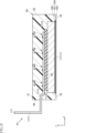
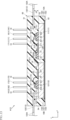
図1は、半導体装置A10を示す平面図である。図2は、半導体装置A10を示す底面図である。図3は、半導体装置A10を示す側面図である。図4は、図1のIV-IV線に沿う断面図である。図5は、図1のV-V線に沿う断面図である。図6は、図1のVI-VI線に沿う断面図である。図7は、図1のVII-VII線に沿う断面図である。図8は、図1のVIII-VIII線に沿う断面図である。図9は、図1のIX-IX線に沿う断面図である。図10は、図1のX-X線に沿う断面図である。図11は、図1のXI-XI線に沿う断面図である。これらの図において、z方向は、例えば本開示の厚さ方向の一例である。図1においては、封止樹脂50を想像線で示している。
1 is a plan view of the semiconductor device A10. FIG. 2 is a bottom view of the semiconductor device A10. FIG. 3 is a side view of the semiconductor device A10. FIG. 4 is a cross-sectional view taken along line IV-IV in FIG. 1. FIG. 5 is a cross-sectional view taken along line V-V in FIG. 1. FIG. 6 is a cross-sectional view taken along line VI-VI in FIG. 1. FIG. 7 is a cross-sectional view taken along line VII-VII in FIG. 1. FIG. 8 is a cross-sectional view taken along line VIII-VIII in FIG. 1. FIG. 9 is a cross-sectional view taken along line IX-IX in FIG. 1. FIG. 10 is a cross-sectional view taken along line X-X in FIG. 1. FIG. 11 is a cross-sectional view taken along line XI-XI in FIG. 1. In these figures, the z direction is, for example, an example of the thickness direction of the present disclosure. In FIG. 1, the sealing resin 50 is shown by imaginary lines.
導電部材11:
導電部材11は、第1金属層111、第1端子112および第1ダンネージ材113を含む。第1金属層111は、導電性材料であり、たとえばCu(銅)を含む。第1金属層111は、半導体装置A10のx方向の一方側に位置する。第1金属層111は、第1主面111Aを有する。第1主面111Aは、z方向の一方側を向く。図示された例においては、第1主面111Aは、平坦面である。 Conductive member 11:
Theconductive member 11 includes a first metal layer 111, a first terminal 112, and a first dunnage material 113. The first metal layer 111 is a conductive material, and includes, for example, Cu (copper). The first metal layer 111 is located on one side in the x-direction of the semiconductor device A10. The first metal layer 111 has a first main surface 111A. The first main surface 111A faces one side in the z-direction. In the illustrated example, the first main surface 111A is a flat surface.
導電部材11は、第1金属層111、第1端子112および第1ダンネージ材113を含む。第1金属層111は、導電性材料であり、たとえばCu(銅)を含む。第1金属層111は、半導体装置A10のx方向の一方側に位置する。第1金属層111は、第1主面111Aを有する。第1主面111Aは、z方向の一方側を向く。図示された例においては、第1主面111Aは、平坦面である。 Conductive member 11:
The
第1端子112は、図1、図2および図6に示すように、x方向の一方側に突出しており、封止樹脂50から露出した部位を有する。第1端子112は、封止樹脂50からx方向の一方側に突出して露出した部位を有する。第1端子112は、第1金属層111のx方向の一方側に位置している。第1端子112は、第1金属層111のy方向の他方側に位置している。第1端子112のx方向の他方側の一部は、第1金属層111のy方向の他方側の一部に、z方向において重なっている。第1端子112は、第1主面111Aに対してz方向の一方側に位置し、第1金属層111から離れている。第1端子112のx方向の他方側の一部は、第1主面111Aのx方向の一方側の一部に、z方向に視て重なっている。第1端子112の組成は、Cu(銅)を含む。第1端子112には、第1取付け孔112Aを有する。第1取付け孔112Aは、第1端子112をz方向に貫通している。
1, 2 and 6, the first terminal 112 protrudes to one side in the x direction and has a portion exposed from the sealing resin 50. The first terminal 112 protrudes to one side in the x direction from the sealing resin 50 and has a portion exposed. The first terminal 112 is located on one side in the x direction of the first metal layer 111. The first terminal 112 is located on the other side in the y direction of the first metal layer 111. A portion of the first terminal 112 on the other side in the x direction overlaps with a portion of the first metal layer 111 on the other side in the y direction in the z direction. The first terminal 112 is located on one side in the z direction with respect to the first main surface 111A and is separated from the first metal layer 111. A portion of the first terminal 112 on the other side in the x direction overlaps with a portion of the first main surface 111A on one side in the x direction when viewed in the z direction. The composition of the first terminal 112 includes Cu (copper). The first terminal 112 has a first mounting hole 112A. The first mounting hole 112A penetrates the first terminal 112 in the z direction.
第1ダンネージ材113は、図1および図6に示すように、第1金属層111と第1端子112との間に介在している。第1ダンネージ材113の組成は、Cu(銅)を含む。第1ダンネージ材113は、第1金属層111の第1主面111Aおよび第1端子112に導通接合されている。導通接合の手法は何ら限定されず、はんだ等の導電性接合材を用いた手法、溶接等の手法、等を適宜採用すればよい。
As shown in Figs. 1 and 6, the first dunnage material 113 is interposed between the first metal layer 111 and the first terminal 112. The composition of the first dunnage material 113 includes Cu (copper). The first dunnage material 113 is conductively joined to the first main surface 111A of the first metal layer 111 and the first terminal 112. There are no limitations on the method of conductive joining, and a method using a conductive bonding material such as solder, a method such as welding, etc. may be appropriately adopted.
本実施形態においては、図1、図2および図4~図9に示すように、第1金属層111は、支持部材10Aによって支持されている。支持部材10Aは、第1金属層111に対して第1主面111Aとは反対側に位置している。支持部材10Aの具体的構成は何ら限定されず、本実施形態においては、支持部材10Aは、DBC(Direct Bonded Copper)基板、AMB(Active Metal Brazing)基板等から構成される。支持部材10Aは、絶縁層101、支持層102および放熱層103を含む。支持部材10Aは、放熱層103の一部を除き封止樹脂50に覆われている。
In this embodiment, as shown in Figures 1, 2, and 4 to 9, the first metal layer 111 is supported by a support member 10A. The support member 10A is located on the opposite side of the first metal layer 111 from the first main surface 111A. There are no limitations on the specific configuration of the support member 10A, and in this embodiment, the support member 10A is composed of a DBC (Direct Bonded Copper) substrate, an AMB (Active Metal Brazing) substrate, or the like. The support member 10A includes an insulating layer 101, a support layer 102, and a heat dissipation layer 103. The support member 10A is covered with a sealing resin 50 except for a portion of the heat dissipation layer 103.
絶縁層101は、z方向において支持層102と放熱層103との間に位置する部分を含む。絶縁層101は、熱伝導率が高い材料としうる。絶縁層101は、たとえば、窒化アルミニウム(AlN)焼結体を含むセラミックスとしうる。絶縁層101の厚さは、第1金属層111の厚さより薄い。
The insulating layer 101 includes a portion located between the support layer 102 and the heat dissipation layer 103 in the z direction. The insulating layer 101 may be a material with high thermal conductivity. The insulating layer 101 may be, for example, a ceramic including an aluminum nitride (AlN) sintered body. The thickness of the insulating layer 101 is thinner than the thickness of the first metal layer 111.
支持層102は、z方向において絶縁層101と、第1金属層111との間に位置する。支持層102の組成は、銅(Cu)を含む。z方向に視て、支持層102の外周は、絶縁層101の外周より内側に位置する。支持層102は、第1金属層111に接合されている。支持層102と第1金属層111との接合は、たとえばはんだを介する。
The support layer 102 is located between the insulating layer 101 and the first metal layer 111 in the z direction. The composition of the support layer 102 includes copper (Cu). When viewed in the z direction, the outer periphery of the support layer 102 is located inside the outer periphery of the insulating layer 101. The support layer 102 is bonded to the first metal layer 111. The support layer 102 and the first metal layer 111 are bonded, for example, via solder.
放熱層103は、z方向において絶縁層101を基準として支持層102とは反対側に位置する。放熱層103の一部は、封止樹脂50から露出している。半導体装置A10の使用の際、放熱層103には、たとえばヒートシンク(図示略)が接合される。放熱層103の組成は、銅を含む。z方向に視て、放熱層103の外周は、絶縁層101の外周より内側に位置する。
The heat dissipation layer 103 is located on the opposite side of the insulating layer 101 from the support layer 102 in the z direction. A part of the heat dissipation layer 103 is exposed from the sealing resin 50. When the semiconductor device A10 is in use, for example, a heat sink (not shown) is joined to the heat dissipation layer 103. The composition of the heat dissipation layer 103 includes copper. When viewed in the z direction, the outer periphery of the heat dissipation layer 103 is located inside the outer periphery of the insulating layer 101.
導電部材12:
導電部材12は、第2金属層121、第2端子122および第2ダンネージ材123を含む。第2金属層121は、導電性材料であり、たとえばCu(銅)を含む。第2金属層121は、半導体装置A10のx方向の他方側に位置する。第2金属層121は、第2主面121Aを有する。第2主面121Aは、z方向の一方側を向く。図示された例においては、第2主面121Aは、平坦面である。 Conductive member 12:
Theconductive member 12 includes a second metal layer 121, a second terminal 122, and a second dunnage material 123. The second metal layer 121 is a conductive material, and includes, for example, Cu (copper). The second metal layer 121 is located on the other side of the semiconductor device A10 in the x direction. The second metal layer 121 has a second main surface 121A. The second main surface 121A faces one side in the z direction. In the illustrated example, the second main surface 121A is a flat surface.
導電部材12は、第2金属層121、第2端子122および第2ダンネージ材123を含む。第2金属層121は、導電性材料であり、たとえばCu(銅)を含む。第2金属層121は、半導体装置A10のx方向の他方側に位置する。第2金属層121は、第2主面121Aを有する。第2主面121Aは、z方向の一方側を向く。図示された例においては、第2主面121Aは、平坦面である。 Conductive member 12:
The
第2端子122は、図1~図6に示すように、x方向の他方側に突出しており、封止樹脂50から露出した部位を有する。第2端子122は、封止樹脂50からx方向の他方側に突出して露出した部位を有する。第2端子122は、第2金属層121のx方向の他方側に位置している。第1端子112のx方向の一方側の一部は、第2金属層121のx方向の他方側の一部に、z方向において重なっている。第2端子122のy方向の中心位置は、第2金属層121のy方向の中心位置とほぼ一致している。第2端子122は、第2主面121Aに対してz方向の一方側に位置し、第2金属層121から離れている。第2端子122のx方向の一方側の一部は、第2主面121Aのy方向における中心部に、z方向に視て重なっている。第2端子122の組成は、Cu(銅)を含む。第2端子122には、第2取付け孔122Aが設けられている。第2取付け孔122Aは、第2端子122をz方向に貫通している。
As shown in Figures 1 to 6, the second terminal 122 protrudes to the other side in the x direction and has a portion exposed from the sealing resin 50. The second terminal 122 protrudes to the other side in the x direction from the sealing resin 50 and has an exposed portion. The second terminal 122 is located on the other side in the x direction of the second metal layer 121. A portion of one side of the first terminal 112 in the x direction overlaps in the z direction with a portion of the other side in the x direction of the second metal layer 121. The center position of the second terminal 122 in the y direction approximately coincides with the center position of the second metal layer 121 in the y direction. The second terminal 122 is located on one side in the z direction with respect to the second main surface 121A and is separated from the second metal layer 121. A portion of one side of the second terminal 122 in the x direction overlaps with the center of the second main surface 121A in the y direction when viewed in the z direction. The composition of the second terminal 122 includes Cu (copper). The second terminal 122 has a second mounting hole 122A. The second mounting hole 122A penetrates the second terminal 122 in the z direction.
第2ダンネージ材123は、図1および図4~図6に示すように、第2金属層121と第2端子122との間に介在している。第2ダンネージ材123の組成は、Cu(銅)を含む。第2ダンネージ材123は、第2金属層121の第2主面121Aおよび第2端子122に導通接合されている。導通接合の手法は何ら限定されず、はんだ等の導電性接合材を用いた手法、溶接等の手法、等を適宜採用すればよい。
The second dunnage material 123 is interposed between the second metal layer 121 and the second terminal 122, as shown in FIG. 1 and FIG. 4 to FIG. 6. The composition of the second dunnage material 123 includes Cu (copper). The second dunnage material 123 is conductively joined to the second main surface 121A of the second metal layer 121 and the second terminal 122. There are no limitations on the method of conductive joining, and a method using a conductive joining material such as solder, a method such as welding, etc. may be appropriately adopted.
本実施形態においては、図1、図2、図4~図6、図10および図11に示すように、第2金属層121は、支持部材10Bによって支持されている。支持部材10Bは、第2金属層121に対して第2主面121Aとは反対側に位置している。支持部材10Aの具体的構成は何ら限定されず、本実施形態においては、支持部材10Aと同様の構成であり、その説明を省略する。
In this embodiment, as shown in Figures 1, 2, 4 to 6, 10, and 11, the second metal layer 121 is supported by a support member 10B. The support member 10B is located on the opposite side of the second metal layer 121 from the second main surface 121A. There are no limitations on the specific configuration of the support member 10A, and in this embodiment, it has the same configuration as the support member 10A, so a description of this will be omitted.
第1半導体素子21:
複数の第1半導体素子21は、図1および図4~図7に示すように、第1金属層111の第1主面111Aに接合されている。複数の第1半導体素子21は、いずれも同一の素子である。各第1半導体素子21は、たとえばMOSFET(Metal-Oxide-Semiconductor Field-Effect Transistor)、MISFET(Metal-Insulator-Semiconductor Field-Effect Transistor)を含む電界効果トランジスタ、およびIGBT(Insulated Gate Bipolar Transistor)のようなバイポーラトランジスタのいずれかとしうる。各第1半導体素子21は、本実施形態と異なり、ダイオードとしうる。半導体装置A10の説明においては、複数の第1半導体素子21は、nチャネル型であり、かつ縦型構造のMOSFETを対象とする。複数の第1半導体素子21は、化合物半導体基板を含む。当該化合物半導体基板の組成は、炭化ケイ素(SiC)を含む。複数の第1半導体素子21は、第1主面111Aの上に、y方向に沿って並んでいる。 First semiconductor element 21:
As shown in FIG. 1 and FIG. 4 to FIG. 7, thefirst semiconductor elements 21 are bonded to the first main surface 111A of the first metal layer 111. The first semiconductor elements 21 are all identical elements. Each of the first semiconductor elements 21 may be, for example, a field effect transistor including a metal-oxide-semiconductor field-effect transistor (MOSFET) or a metal-insulator-semiconductor field-effect transistor (MISFET), or a bipolar transistor such as an insulated gate bipolar transistor (IGBT). Unlike the present embodiment, each of the first semiconductor elements 21 may be a diode. In the description of the semiconductor device A10, the first semiconductor elements 21 are n-channel type MOSFETs having a vertical structure. The first semiconductor elements 21 include a compound semiconductor substrate. The composition of the compound semiconductor substrate includes silicon carbide (SiC). The first semiconductor elements 21 are arranged on the first main surface 111A along the y direction.
複数の第1半導体素子21は、図1および図4~図7に示すように、第1金属層111の第1主面111Aに接合されている。複数の第1半導体素子21は、いずれも同一の素子である。各第1半導体素子21は、たとえばMOSFET(Metal-Oxide-Semiconductor Field-Effect Transistor)、MISFET(Metal-Insulator-Semiconductor Field-Effect Transistor)を含む電界効果トランジスタ、およびIGBT(Insulated Gate Bipolar Transistor)のようなバイポーラトランジスタのいずれかとしうる。各第1半導体素子21は、本実施形態と異なり、ダイオードとしうる。半導体装置A10の説明においては、複数の第1半導体素子21は、nチャネル型であり、かつ縦型構造のMOSFETを対象とする。複数の第1半導体素子21は、化合物半導体基板を含む。当該化合物半導体基板の組成は、炭化ケイ素(SiC)を含む。複数の第1半導体素子21は、第1主面111Aの上に、y方向に沿って並んでいる。 First semiconductor element 21:
As shown in FIG. 1 and FIG. 4 to FIG. 7, the
第1半導体素子21の各々は、第1ドレイン電極211、第1ソース電極212および第1ゲート電極213を有する。
Each of the first semiconductor elements 21 has a first drain electrode 211, a first source electrode 212, and a first gate electrode 213.
第1ドレイン電極211は、第1半導体素子21において、z方向の他方側に位置する。第1ドレイン電極211は、第1金属層111の第1主面111Aに対向している。第1ドレイン電極211には、第1半導体素子21により変換される前の電力に対応する電流が流れるように構成される。第1ドレイン電極211は、導電接合層29を介して第1主面111Aに導電接合されている。複数の第1半導体素子21の各第1ドレイン電極211は、導電部材11に導通している。導電接合層29は、たとえばハンダ、および銀などを含む焼結金属のいずれかとしうる。
The first drain electrode 211 is located on the other side in the z direction of the first semiconductor element 21. The first drain electrode 211 faces the first main surface 111A of the first metal layer 111. The first drain electrode 211 is configured to allow a current corresponding to the power before being converted by the first semiconductor element 21 to flow through it. The first drain electrode 211 is conductively bonded to the first main surface 111A via a conductive bonding layer 29. Each of the first drain electrodes 211 of the multiple first semiconductor elements 21 is conductive to the conductive member 11. The conductive bonding layer 29 can be, for example, either solder or a sintered metal including silver or the like.
第1ソース電極212は、第1半導体素子21において、z方向の一方側に位置する。第1ソース電極212は、z方向において第1ドレイン電極211と反対側に位置する。第1ソース電極212には、第1半導体素子21により変換された後の電力に対応する電流が流れるように構成される。
The first source electrode 212 is located on one side of the first semiconductor element 21 in the z direction. The first source electrode 212 is located on the opposite side of the first drain electrode 211 in the z direction. The first source electrode 212 is configured to allow a current corresponding to the power converted by the first semiconductor element 21 to flow through it.
第1ゲート電極213は、第1半導体素子21において、z方向の一方側に位置する。第1ゲート電極213は、第1半導体素子21において、z方向において第1ソース電極212と同じ側に位置する。第1ゲート電極213には、第1半導体素子21を駆動するためのゲート電圧が印加されるように構成される。図3に示すように、z方向に視て、第1ゲート電極213の面積は、第1ソース電極212の面積より小さい。
The first gate electrode 213 is located on one side of the first semiconductor element 21 in the z direction. The first gate electrode 213 is located on the same side of the first semiconductor element 21 as the first source electrode 212 in the z direction. The first gate electrode 213 is configured to receive a gate voltage for driving the first semiconductor element 21. As shown in FIG. 3, the area of the first gate electrode 213 is smaller than the area of the first source electrode 212 when viewed in the z direction.
第2半導体素子22:
複数の第2半導体素子22は、図1および図4~図6に示すように、第2金属層121の第2主面121Aに接合されている。複数の第2半導体素子22は、複数の第1半導体素子21と同一の素子である。各第2半導体素子22は、nチャネル型であり、かつ縦型構造のMOSFETとしうる。各第2半導体素子22は、MISFET(Metal-Insulator-Semiconductor Field-Effect Transistor)を含む電界効果トランジスタ、およびIGBT(Insulated Gate Bipolar Transistor)のようなバイポーラトランジスタのいずれかとしうる。各第2半導体素子22は、ダイオードとしうる。半導体装置A10の説明においては、複数の第2半導体素子22は、nチャネル型であり、かつ縦型構造のMOSFETを対象とする。複数の第2半導体素子22は、化合物半導体基板を含む。当該化合物半導体基板の組成は、炭化ケイ素(SiC)を含む。複数の第2半導体素子22は、第2主面121Aの上に、y方向に沿って並んでいる。 Second semiconductor element 22:
Thesecond semiconductor elements 22 are bonded to the second main surface 121A of the second metal layer 121 as shown in FIG. 1 and FIG. 4 to FIG. 6. The second semiconductor elements 22 are the same elements as the first semiconductor elements 21. Each of the second semiconductor elements 22 may be an n-channel type MOSFET having a vertical structure. Each of the second semiconductor elements 22 may be either a field effect transistor including a metal-insulator-semiconductor field-effect transistor (MISFET) or a bipolar transistor such as an insulated gate bipolar transistor (IGBT). Each of the second semiconductor elements 22 may be a diode. In the description of the semiconductor device A10, the second semiconductor elements 22 are n-channel type MOSFETs having a vertical structure. The second semiconductor elements 22 include a compound semiconductor substrate. The composition of the compound semiconductor substrate includes silicon carbide (SiC). The multiple second semiconductor elements 22 are arranged on the second main surface 121A along the y direction.
複数の第2半導体素子22は、図1および図4~図6に示すように、第2金属層121の第2主面121Aに接合されている。複数の第2半導体素子22は、複数の第1半導体素子21と同一の素子である。各第2半導体素子22は、nチャネル型であり、かつ縦型構造のMOSFETとしうる。各第2半導体素子22は、MISFET(Metal-Insulator-Semiconductor Field-Effect Transistor)を含む電界効果トランジスタ、およびIGBT(Insulated Gate Bipolar Transistor)のようなバイポーラトランジスタのいずれかとしうる。各第2半導体素子22は、ダイオードとしうる。半導体装置A10の説明においては、複数の第2半導体素子22は、nチャネル型であり、かつ縦型構造のMOSFETを対象とする。複数の第2半導体素子22は、化合物半導体基板を含む。当該化合物半導体基板の組成は、炭化ケイ素(SiC)を含む。複数の第2半導体素子22は、第2主面121Aの上に、y方向に沿って並んでいる。 Second semiconductor element 22:
The
複数の第2半導体素子22の各々は、第2ドレイン電極221、第2ソース電極222および第2ゲート電極223を有する。
Each of the multiple second semiconductor elements 22 has a second drain electrode 221, a second source electrode 222, and a second gate electrode 223.
第2ドレイン電極221は、第2半導体素子22において、z方向の一方側に位置する。第2ゲート電極223は、第2半導体素子22において、第2金属層121の第2主面121Aに対向している。第2ドレイン電極221には、第2半導体素子22により変換される前の電力に対応する電流が流れるように構成される。第2ドレイン電極221は、導電接合層29を介して第2主面121Aに導電接合されている。複数の第2半導体素子22の各第2ドレイン電極221は、導電部材12に導通している。
The second drain electrode 221 is located on one side in the z direction in the second semiconductor element 22. The second gate electrode 223 faces the second main surface 121A of the second metal layer 121 in the second semiconductor element 22. The second drain electrode 221 is configured so that a current corresponding to the power before being converted by the second semiconductor element 22 flows through it. The second drain electrode 221 is conductively bonded to the second main surface 121A via the conductive bonding layer 29. Each of the second drain electrodes 221 of the multiple second semiconductor elements 22 is electrically connected to the conductive member 12.
第2ソース電極222は、第2半導体素子22において、z方向の一方側に位置する。第2ソース電極222は、第2半導体素子22において、z方向において第2ドレイン電極221と反対側に位置する。第2ソース電極222には、第2半導体素子22により変換された後の電力に対応する電流が流れるように構成される。
The second source electrode 222 is located on one side of the second semiconductor element 22 in the z direction. The second source electrode 222 is located on the opposite side of the second drain electrode 221 in the z direction of the second semiconductor element 22. The second source electrode 222 is configured to allow a current corresponding to the power converted by the second semiconductor element 22 to flow through it.
第2ゲート電極223は、第2半導体素子22において、z方向の一方側に位置する。第2ソース電極222は、第2半導体素子22において、z方向において第2ソース電極222と同じ側に位置する。第2ゲート電極223には、第2半導体素子22を駆動するためのゲート電圧が印加されるように構成される。z方向に視て、第2ゲート電極223の面積は、第2ソース電極222の面積より小さい。
The second gate electrode 223 is located on one side of the second semiconductor element 22 in the z direction. The second source electrode 222 is located on the same side of the second semiconductor element 22 as the second source electrode 222 in the z direction. The second gate electrode 223 is configured to receive a gate voltage for driving the second semiconductor element 22. When viewed in the z direction, the area of the second gate electrode 223 is smaller than the area of the second source electrode 222.
第1導電部材13:
第1導電部材13は、図1、図2、図4~図7に示すように、延出部131および第3端子132を含む。第1導電部材13は、導電性材料であり、たとえばCu(銅)を含む。 First conductive member 13:
1, 2, and 4 to 7, the firstconductive member 13 includes an extension 131 and a third terminal 132. The first conductive member 13 is a conductive material and includes, for example, Cu (copper).
第1導電部材13は、図1、図2、図4~図7に示すように、延出部131および第3端子132を含む。第1導電部材13は、導電性材料であり、たとえばCu(銅)を含む。 First conductive member 13:
1, 2, and 4 to 7, the first
第3端子132は、封止樹脂50からx方向の一方側に突出した部位を有する。第3端子132は、封止樹脂50からx方向の一方側に突出して露出した部位を有する。第3端子132は、第1端子112に対してy方向の一方側に位置する。第3端子132は、第1金属層111のx方向の一方側に位置している。第3端子132は、第1主面111Aに対してz方向の一方側に位置し、第1金属層111から離れている。第3端子132のx方向の他方側の一部は、第1主面111Aのx方向の一方側の一部に、z方向に視て重なっている。第3端子132の組成は、Cu(銅)を含む。第3端子132には、第3取付け孔132Aを有する。第3取付け孔132Aは、第3端子132をz方向に貫通している。
The third terminal 132 has a portion protruding from the sealing resin 50 to one side in the x direction. The third terminal 132 has a portion protruding from the sealing resin 50 to one side in the x direction and exposed. The third terminal 132 is located on one side in the y direction with respect to the first terminal 112. The third terminal 132 is located on one side in the x direction of the first metal layer 111. The third terminal 132 is located on one side in the z direction with respect to the first main surface 111A and is separated from the first metal layer 111. A portion of the other side in the x direction of the third terminal 132 overlaps a portion of the one side in the x direction of the first main surface 111A when viewed in the z direction. The composition of the third terminal 132 includes Cu (copper). The third terminal 132 has a third mounting hole 132A. The third mounting hole 132A penetrates the third terminal 132 in the z direction.
延出部131は、第3端子132からx方向の他方側に延出している。延出部131は、封止樹脂50によって覆われている。本実施形態の延出部131は、第1部1311、第2部1312および第3部1313を含む。
The extension portion 131 extends from the third terminal 132 to the other side in the x-direction. The extension portion 131 is covered with the sealing resin 50. In this embodiment, the extension portion 131 includes a first portion 1311, a second portion 1312, and a third portion 1313.
第1部1311は、図4および図5に示すように、z方向における第1主面111Aからの距離z1が、z方向における第1主面111Aから第3端子132までの距離z0より小さい。距離z1の大きさは、たとえば0.1mm以上である。第1部1311は、図1、図2、図4~図7に示すように、x方向において複数の第1半導体素子21と複数の第2半導体素子22との間に位置する。図5に示すように、図示された例においては、距離z1は、z方向における第1主面111Aから第1半導体素子21のz方向の一方側端までの距離z2より大きい。たとえば、距離z2が0.5mm程度であるのに対し、距離z1は、0.8mm~1.2mm程度である。
As shown in Figures 4 and 5, the distance z1 of the first portion 1311 from the first main surface 111A in the z direction is smaller than the distance z0 from the first main surface 111A to the third terminal 132 in the z direction. The magnitude of the distance z1 is, for example, 0.1 mm or more. As shown in Figures 1, 2, and 4 to 7, the first portion 1311 is located between the multiple first semiconductor elements 21 and the multiple second semiconductor elements 22 in the x direction. As shown in Figure 5, in the illustrated example, the distance z1 is larger than the distance z2 from the first main surface 111A in the z direction to one side end of the first semiconductor element 21 in the z direction. For example, the distance z2 is about 0.5 mm, while the distance z1 is about 0.8 mm to 1.2 mm.
第1部1311の形状は何ら限定されず、本実施形態においては、y方向に延びる形状である。第1部1311は、たとえば平坦な帯状である。図示された例においては、第1部1311は、z方向に視て、第1主面111A(第1金属層111)と重なる。図示された例においては、第1部1311のx方向の他方側端縁は、第1主面111Aのx方向の他方側端縁よりx方向の一方側に位置している。
The shape of the first portion 1311 is not limited in any way, and in this embodiment, it is a shape that extends in the y direction. The first portion 1311 is, for example, a flat band shape. In the illustrated example, the first portion 1311 overlaps with the first main surface 111A (first metal layer 111) when viewed in the z direction. In the illustrated example, the other end edge of the first portion 1311 in the x direction is located on one side in the x direction of the other end edge of the first main surface 111A in the x direction.
第2部1312は、第3端子132に繋がっている。第2部1312は、第3端子132からx方向の他方側にx方向に沿って延びている。第2部1312の形状は何ら限定されず、たとえば平坦な帯状である。z方向における第1主面111Aから第2部1312までの距離は、距離z0と同じ(あるいは略同じ)である。第2部1312は、複数の第1半導体素子21に対してy方向の一方側(図1における図中右側)に位置している。第2部1312のx方向の他方側端縁は、第1半導体素子21のx方向の一方側端縁よりx方向の他方側に位置している。
The second portion 1312 is connected to the third terminal 132. The second portion 1312 extends from the third terminal 132 along the x direction to the other side in the x direction. The shape of the second portion 1312 is not limited in any way, and may be, for example, a flat band. The distance in the z direction from the first main surface 111A to the second portion 1312 is the same as (or approximately the same as) the distance z0. The second portion 1312 is located on one side in the y direction (the right side in FIG. 1) with respect to the multiple first semiconductor elements 21. The other edge in the x direction of the second portion 1312 is located on the other side in the x direction of the one edge in the x direction of the first semiconductor element 21.
第3部1313は、第1部1311と第2部1312との間に介在している。第3部1313を有することにより、延出部131は、y方向に視て屈曲形状である。図示された例においては、第3部1313は、第1部1311のx方向の一方側端縁の一部であって、y方向の一方側端寄りの部分に繋がっている。第3部1313は、第2部1312のx方向の他方側の部分に繋がっている。
The third portion 1313 is interposed between the first portion 1311 and the second portion 1312. By having the third portion 1313, the extension portion 131 has a bent shape when viewed in the y direction. In the illustrated example, the third portion 1313 is part of one side edge of the first portion 1311 in the x direction, and is connected to a portion closer to one side end in the y direction. The third portion 1313 is connected to a portion of the second portion 1312 on the other side in the x direction.
第1接続部材14:
複数の第1接続部材14は、図1、図5および図7に示すように、複数の第1半導体素子21と導電部材12とを個別に導通させている。より具体的には、第1接続部材14は、第1半導体素子21の第1ソース電極212と、第2金属層121の第2主面121Aとに接続されている。第1接続部材14の具体的構成は何ら限定されず、たとえば金属材料を含むワイヤおよびリボン等である。金属材料は、たとえば、Cu(銅)、Al(アルミ)等やこれらの合金等を含む。本例の第1接続部材14は、Cu(銅)を含むワイヤである。第1接続部材14の個数は何ら限定されず、図示された例においては、1つの第1半導体素子21の第1ソース電極212と第1金属層111の第1主面111Aとに2つの第1接続部材14が接続されている。 First connecting member 14:
As shown in FIG. 1, FIG. 5, and FIG. 7, thefirst connection members 14 individually conduct the first semiconductor elements 21 and the conductive member 12. More specifically, the first connection members 14 are connected to the first source electrode 212 of the first semiconductor element 21 and the second main surface 121A of the second metal layer 121. The specific configuration of the first connection members 14 is not limited, and may be, for example, a wire or ribbon containing a metal material. The metal material may include, for example, Cu (copper), Al (aluminum), or an alloy thereof. The first connection members 14 in this example are wires containing Cu (copper). The number of the first connection members 14 is not limited, and in the illustrated example, two first connection members 14 are connected to the first source electrode 212 of one first semiconductor element 21 and the first main surface 111A of the first metal layer 111.
複数の第1接続部材14は、図1、図5および図7に示すように、複数の第1半導体素子21と導電部材12とを個別に導通させている。より具体的には、第1接続部材14は、第1半導体素子21の第1ソース電極212と、第2金属層121の第2主面121Aとに接続されている。第1接続部材14の具体的構成は何ら限定されず、たとえば金属材料を含むワイヤおよびリボン等である。金属材料は、たとえば、Cu(銅)、Al(アルミ)等やこれらの合金等を含む。本例の第1接続部材14は、Cu(銅)を含むワイヤである。第1接続部材14の個数は何ら限定されず、図示された例においては、1つの第1半導体素子21の第1ソース電極212と第1金属層111の第1主面111Aとに2つの第1接続部材14が接続されている。 First connecting member 14:
As shown in FIG. 1, FIG. 5, and FIG. 7, the
第1接続部材14は、第1部1311をz方向の一方側に跨いでいる。すなわち、第1接続部材14は、第1部1311に対してz方向の一方側に離れている部位を有する。図示された例においては、第1接続部材14は、第1部1311をz方向の一方側に跨ぐ湾曲形状である。
The first connecting member 14 straddles the first portion 1311 to one side in the z direction. That is, the first connecting member 14 has a portion that is separated from the first portion 1311 to one side in the z direction. In the illustrated example, the first connecting member 14 has a curved shape that straddles the first portion 1311 to one side in the z direction.
第2接続部材15:
複数の第2接続部材15は、図1、図4、図6および図7に示すように、複数の第2半導体素子22と第1導電部材13とを個別に導通させている。より具体的には、第2接続部材15は、第2半導体素子22の第2ソース電極222と、第1導電部材13の延出部131の第1部1311とに接続されている。複数の第2接続部材15の具体的構成は何ら限定されず、たとえば金属材料を含むワイヤおよびリボン、あるいは板材料等としうる。第2接続部材15は、第1導電部材13と別体であってよいし、第1導電部材13と一体であってよい。本実施形態においては、第2接続部材15は、第1導電部材13と別体であり、たとえばCu(銅)を含むワイヤである。第2接続部材15の個数は何ら限定されず、図示された例においては、1つの第2半導体素子22の第2ソース電極222と、第2金属層121の第2主面121Aとに2つの第2接続部材15が接続されている。 Second connecting member 15:
As shown in FIGS. 1, 4, 6 and 7, thesecond connection members 15 individually conduct the second semiconductor elements 22 and the first conductive member 13. More specifically, the second connection members 15 are connected to the second source electrode 222 of the second semiconductor element 22 and the first portion 1311 of the extension portion 131 of the first conductive member 13. The specific configuration of the second connection members 15 is not limited in any way, and may be, for example, a wire and ribbon containing a metal material, or a plate material. The second connection members 15 may be separate from the first conductive member 13, or may be integrated with the first conductive member 13. In this embodiment, the second connection members 15 are separate from the first conductive member 13 and are, for example, wires containing Cu (copper). The number of second connection members 15 is not limited in any way, and in the example shown, two second connection members 15 are connected to the second source electrode 222 of one second semiconductor element 22 and the second main surface 121A of the second metal layer 121.
複数の第2接続部材15は、図1、図4、図6および図7に示すように、複数の第2半導体素子22と第1導電部材13とを個別に導通させている。より具体的には、第2接続部材15は、第2半導体素子22の第2ソース電極222と、第1導電部材13の延出部131の第1部1311とに接続されている。複数の第2接続部材15の具体的構成は何ら限定されず、たとえば金属材料を含むワイヤおよびリボン、あるいは板材料等としうる。第2接続部材15は、第1導電部材13と別体であってよいし、第1導電部材13と一体であってよい。本実施形態においては、第2接続部材15は、第1導電部材13と別体であり、たとえばCu(銅)を含むワイヤである。第2接続部材15の個数は何ら限定されず、図示された例においては、1つの第2半導体素子22の第2ソース電極222と、第2金属層121の第2主面121Aとに2つの第2接続部材15が接続されている。 Second connecting member 15:
As shown in FIGS. 1, 4, 6 and 7, the
図1に示すように、複数の第1接続部材14と複数の第2接続部材15とは、y方向に並んでいる。図示された例においては、2つずつの第1接続部材14と2つずつの第2接続部材15とが、交互にy方向に並んでいる。
As shown in FIG. 1, the multiple first connection members 14 and the multiple second connection members 15 are aligned in the y direction. In the illustrated example, two first connection members 14 and two second connection members 15 are aligned alternately in the y direction.
第2導電部材171,第4導電部材181:
第2導電部材171は、図1~図6および図9に示すように、第1ゲート端子1711、第1ゲート配線部1712および段差部1713を含む。第2導電部材171は、いわゆるリード部材であり、組成にたとえばCu(銅)を含む。第1ゲート端子1711は、封止樹脂50の外部に位置しており、半導体装置A10の複数の第1半導体素子21にゲート電圧を供給可能なゲート端子として機能する。第1ゲート配線部1712は、複数の第1半導体素子21に対してx方向の一方側に位置している。第1ゲート配線部1712は、第1金属層111の第1主面111Aからz方向の一方側に離れている。第1ゲート配線部1712は、y方向に延びた形状である。z方向における第1主面111Aから第1ゲート配線部1712までの距離は、z方向における第1主面111Aから第1ゲート端子1711までの距離より小さい。第1ゲート配線部1712は、複数の第3接続部材41によって、複数の第1半導体素子21の各第1ゲート電極213と個別に導通接続されている。第3接続部材41は、たとえばAu(金)、Cu(銅)等を含むワイヤとしうる。段差部1713は、第1ゲート端子1711と第1ゲート配線部1712との間に位置している。段差部1713を有することにより、第2導電部材171は、x方向に視て屈曲形状としうる。 Secondconductive member 171, fourth conductive member 181:
As shown in FIGS. 1 to 6 and 9, the secondconductive member 171 includes a first gate terminal 1711, a first gate wiring portion 1712, and a step portion 1713. The second conductive member 171 is a so-called lead member, and contains, for example, Cu (copper) in its composition. The first gate terminal 1711 is located outside the sealing resin 50, and functions as a gate terminal capable of supplying a gate voltage to the multiple first semiconductor elements 21 of the semiconductor device A10. The first gate wiring portion 1712 is located on one side in the x direction with respect to the multiple first semiconductor elements 21. The first gate wiring portion 1712 is separated from the first main surface 111A of the first metal layer 111 on one side in the z direction. The first gate wiring portion 1712 has a shape extending in the y direction. The distance from the first main surface 111A to the first gate wiring portion 1712 in the z direction is smaller than the distance from the first main surface 111A to the first gate terminal 1711 in the z direction. The first gate wiring portion 1712 is individually conductively connected to each of the first gate electrodes 213 of the multiple first semiconductor elements 21 by multiple third connection members 41. The third connection members 41 may be wires containing, for example, Au (gold), Cu (copper), or the like. The step portion 1713 is located between the first gate terminal 1711 and the first gate wiring portion 1712. By having the step portion 1713, the second conductive member 171 may have a bent shape when viewed in the x-direction.
第2導電部材171は、図1~図6および図9に示すように、第1ゲート端子1711、第1ゲート配線部1712および段差部1713を含む。第2導電部材171は、いわゆるリード部材であり、組成にたとえばCu(銅)を含む。第1ゲート端子1711は、封止樹脂50の外部に位置しており、半導体装置A10の複数の第1半導体素子21にゲート電圧を供給可能なゲート端子として機能する。第1ゲート配線部1712は、複数の第1半導体素子21に対してx方向の一方側に位置している。第1ゲート配線部1712は、第1金属層111の第1主面111Aからz方向の一方側に離れている。第1ゲート配線部1712は、y方向に延びた形状である。z方向における第1主面111Aから第1ゲート配線部1712までの距離は、z方向における第1主面111Aから第1ゲート端子1711までの距離より小さい。第1ゲート配線部1712は、複数の第3接続部材41によって、複数の第1半導体素子21の各第1ゲート電極213と個別に導通接続されている。第3接続部材41は、たとえばAu(金)、Cu(銅)等を含むワイヤとしうる。段差部1713は、第1ゲート端子1711と第1ゲート配線部1712との間に位置している。段差部1713を有することにより、第2導電部材171は、x方向に視て屈曲形状としうる。 Second
As shown in FIGS. 1 to 6 and 9, the second
第4導電部材181は、図1~図6および図8に示すように、第1検出端子1811、第1検出配線部1812および段差部1813を含む。第4導電部材181は、いわゆるリード部材であり、組成にたとえばCu(銅)を含む。第1検出端子1811は、封止樹脂50の外部に位置しており、半導体装置A10の複数の第1半導体素子21の動作状態を検出可能な検出端子として機能する。第1検出配線部1812は、第1ゲート配線部1712に対してx方向の一方側に位置している。第1検出配線部1812は、第1金属層111の第1主面111Aからz方向の一方側に離れている。第1検出配線部1812は、y方向に延びた形状である。z方向における第1主面111Aから第1検出配線部1812までの距離は、z方向における第1主面111Aから第1検出端子1811までの距離より小さい。第1検出配線部1812は、複数の第5接続部材42によって、複数の第1半導体素子21の各第1ソース電極212と個別に導通接続されている。第5接続部材42は、たとえばAu(金)、Cu(銅)等を含むワイヤとしうる。段差部1813は、第1検出端子1811と第1検出配線部1812との間に位置している。段差部1813を有することにより、第4導電部材181は、x方向に視て屈曲形状としうる。
The fourth conductive member 181 includes a first detection terminal 1811, a first detection wiring portion 1812, and a step portion 1813, as shown in Figures 1 to 6 and 8. The fourth conductive member 181 is a so-called lead member, and contains, for example, Cu (copper) in its composition. The first detection terminal 1811 is located outside the sealing resin 50, and functions as a detection terminal capable of detecting the operating state of the multiple first semiconductor elements 21 of the semiconductor device A10. The first detection wiring portion 1812 is located on one side in the x direction with respect to the first gate wiring portion 1712. The first detection wiring portion 1812 is separated from the first main surface 111A of the first metal layer 111 on one side in the z direction. The first detection wiring portion 1812 has a shape extending in the y direction. The distance from the first main surface 111A to the first detection wiring portion 1812 in the z direction is smaller than the distance from the first main surface 111A to the first detection terminal 1811 in the z direction. The first detection wiring portion 1812 is individually conductively connected to each of the first source electrodes 212 of the first semiconductor elements 21 by a plurality of fifth connection members 42. The fifth connection members 42 may be wires containing, for example, Au (gold), Cu (copper), or the like. The step portion 1813 is located between the first detection terminal 1811 and the first detection wiring portion 1812. By having the step portion 1813, the fourth conductive member 181 may have a bent shape when viewed in the x direction.
第3導電部材172,第5導電部材182:
第3導電部材172は、図1~図6および図10に示すように、第2ゲート端子1721、第2ゲート配線部1722および段差部1723を含む。第3導電部材172は、いわゆるリード部材であり、組成にたとえばCu(銅)を含む。第2ゲート端子1721は、封止樹脂50の外部に位置しており、半導体装置A10の複数の第2半導体素子22にゲート電圧を供給可能なゲート端子として機能する。第2ゲート配線部1722は、複数の第2半導体素子22に対してx方向の他方側に位置している。第2ゲート配線部1722は、第1金属層111の第1主面111Aからz方向の一方側に離れている。第2ゲート配線部1722は、y方向に延びた形状である。z方向における第1主面111Aから第2ゲート配線部1722までの距離は、z方向における第1主面111Aから第2ゲート端子1721までの距離より小さい。第2ゲート配線部1722は、複数の第4接続部材43によって、複数の第2半導体素子22の各第2ゲート電極223と個別に導通接続されている。第4接続部材43は、たとえばAu(金)、Cu(銅)等を含むワイヤとしうる。段差部1723は、第2ゲート端子1721と第2ゲート配線部1722との間に位置している。段差部1723を有することにより、第3導電部材172は、x方向に視て屈曲形状としうる。 Thirdconductive member 172, fifth conductive member 182:
As shown in FIGS. 1 to 6 and 10, the thirdconductive member 172 includes a second gate terminal 1721, a second gate wiring portion 1722, and a step portion 1723. The third conductive member 172 is a so-called lead member, and contains, for example, Cu (copper) in its composition. The second gate terminal 1721 is located outside the sealing resin 50, and functions as a gate terminal capable of supplying a gate voltage to the plurality of second semiconductor elements 22 of the semiconductor device A10. The second gate wiring portion 1722 is located on the other side in the x direction with respect to the plurality of second semiconductor elements 22. The second gate wiring portion 1722 is spaced apart from the first main surface 111A of the first metal layer 111 on one side in the z direction. The second gate wiring portion 1722 has a shape extending in the y direction. The distance from the first main surface 111A to the second gate wiring portion 1722 in the z direction is smaller than the distance from the first main surface 111A to the second gate terminal 1721 in the z direction. The second gate wiring portion 1722 is individually conductively connected to each of the second gate electrodes 223 of the second semiconductor elements 22 by a plurality of fourth connection members 43. The fourth connection members 43 may be wires containing, for example, Au (gold), Cu (copper), or the like. The step portion 1723 is located between the second gate terminal 1721 and the second gate wiring portion 1722. By having the step portion 1723, the third conductive member 172 may have a bent shape when viewed in the x-direction.
第3導電部材172は、図1~図6および図10に示すように、第2ゲート端子1721、第2ゲート配線部1722および段差部1723を含む。第3導電部材172は、いわゆるリード部材であり、組成にたとえばCu(銅)を含む。第2ゲート端子1721は、封止樹脂50の外部に位置しており、半導体装置A10の複数の第2半導体素子22にゲート電圧を供給可能なゲート端子として機能する。第2ゲート配線部1722は、複数の第2半導体素子22に対してx方向の他方側に位置している。第2ゲート配線部1722は、第1金属層111の第1主面111Aからz方向の一方側に離れている。第2ゲート配線部1722は、y方向に延びた形状である。z方向における第1主面111Aから第2ゲート配線部1722までの距離は、z方向における第1主面111Aから第2ゲート端子1721までの距離より小さい。第2ゲート配線部1722は、複数の第4接続部材43によって、複数の第2半導体素子22の各第2ゲート電極223と個別に導通接続されている。第4接続部材43は、たとえばAu(金)、Cu(銅)等を含むワイヤとしうる。段差部1723は、第2ゲート端子1721と第2ゲート配線部1722との間に位置している。段差部1723を有することにより、第3導電部材172は、x方向に視て屈曲形状としうる。 Third
As shown in FIGS. 1 to 6 and 10, the third
第5導電部材182は、図1~図6および図11に示すように、第2検出端子1821、第2検出配線部1822および段差部1823を含む。第5導電部材182は、いわゆるリード部材であり、組成にたとえばCu(銅)を含む。第2検出端子1821は、封止樹脂50の外部に位置しており、半導体装置A10の複数の第2半導体素子22の動作状態を検出可能な検出端子として機能する。第2検出配線部1822は、第2ゲート配線部1722に対してx方向の他方側に位置している。第2検出配線部1822は、第1金属層111の第1主面111Aからz方向の一方側に離れている。第2検出配線部1822は、y方向に延びた形状である。z方向における第1主面111Aから第2検出配線部1822までの距離は、z方向における第1主面111Aから第2検出端子1821までの距離より小さい。第2検出配線部1822は、複数の第6接続部材44によって、複数の第2半導体素子22の第2ソース電極222と個別に導通接続されている。第6接続部材44は、たとえばAu(金)、Cu(銅)等を含むワイヤとしうる。段差部1823は、第2検出端子1821と第2検出配線部1822との間に位置している。段差部1823を有することにより、第5導電部材182は、x方向に視て屈曲形状としうる。
The fifth conductive member 182 includes a second detection terminal 1821, a second detection wiring portion 1822, and a step portion 1823, as shown in Figures 1 to 6 and 11. The fifth conductive member 182 is a so-called lead member, and contains, for example, Cu (copper) in its composition. The second detection terminal 1821 is located outside the sealing resin 50, and functions as a detection terminal capable of detecting the operating state of the multiple second semiconductor elements 22 of the semiconductor device A10. The second detection wiring portion 1822 is located on the other side in the x direction relative to the second gate wiring portion 1722. The second detection wiring portion 1822 is separated from the first main surface 111A of the first metal layer 111 to one side in the z direction. The second detection wiring portion 1822 has a shape extending in the y direction. The distance from the first main surface 111A to the second detection wiring portion 1822 in the z direction is smaller than the distance from the first main surface 111A to the second detection terminal 1821 in the z direction. The second detection wiring portion 1822 is individually conductively connected to the second source electrodes 222 of the second semiconductor elements 22 by a plurality of sixth connection members 44. The sixth connection members 44 may be wires containing, for example, Au (gold), Cu (copper), or the like. The step portion 1823 is located between the second detection terminal 1821 and the second detection wiring portion 1822. By having the step portion 1823, the fifth conductive member 182 may have a bent shape when viewed in the x direction.
ダミー端子19:
半導体装置A10は、図1~図7に示すように、4つのダミー端子19をさらに備える。4つのダミー端子19のうち2つのダミー端子19は、x方向において第1ゲート端子1711および第1検出端子1811を挟んで両側に位置する。残り2つのダミー端子19は、x方向において第2ゲート端子1721および第2検出端子1821を挟んで両側に位置する。ダミー端子19は、金属リードとしうる。ダミー端子19は、銅または銅合金を含む材料としうる。複数のダミー端子19の各々の一部は、封止樹脂に覆われている。複数のダミー端子19のz方向に起立した部分は、封止樹脂50から露出している。 Dummy terminal 19:
The semiconductor device A10 further includes fourdummy terminals 19, as shown in FIGS. 1 to 7. Two of the four dummy terminals 19 are located on both sides of the first gate terminal 1711 and the first detection terminal 1811 in the x direction. The remaining two dummy terminals 19 are located on both sides of the second gate terminal 1721 and the second detection terminal 1821 in the x direction. The dummy terminals 19 may be metal leads. The dummy terminals 19 may be made of a material containing copper or a copper alloy. A portion of each of the multiple dummy terminals 19 is covered with a sealing resin. The portions of the multiple dummy terminals 19 that stand up in the z direction are exposed from the sealing resin 50.
半導体装置A10は、図1~図7に示すように、4つのダミー端子19をさらに備える。4つのダミー端子19のうち2つのダミー端子19は、x方向において第1ゲート端子1711および第1検出端子1811を挟んで両側に位置する。残り2つのダミー端子19は、x方向において第2ゲート端子1721および第2検出端子1821を挟んで両側に位置する。ダミー端子19は、金属リードとしうる。ダミー端子19は、銅または銅合金を含む材料としうる。複数のダミー端子19の各々の一部は、封止樹脂に覆われている。複数のダミー端子19のz方向に起立した部分は、封止樹脂50から露出している。 Dummy terminal 19:
The semiconductor device A10 further includes four
封止樹脂50:
封止樹脂50は、図1~図11に示すように、第1金属層111、第2金属層121、複数の第1接続部材14、複数の第2接続部材15、複数の第1半導体素子21および複数の第2半導体素子22を覆っている。さらに封止樹脂50は、第1端子112、第2端子122、第3端子132の一部ずつと、延出部131、第1ゲート配線部1712、第1検出配線部1812、第2ゲート配線部1722および第2検出配線部1822を覆っている。封止樹脂50は、電気絶縁性を有する。封止樹脂50は、たとえば黒色のエポキシ樹脂を含む材料としうる。封止樹脂50は、頂面51、底面52、第1側面53、第2側面54、第3側面および第4側面56を有する。 Sealing resin 50:
As shown in Figs. 1 to 11, the sealingresin 50 covers the first metal layer 111, the second metal layer 121, the first connection members 14, the second connection members 15, the first semiconductor elements 21, and the second semiconductor elements 22. Furthermore, the sealing resin 50 covers a part of each of the first terminal 112, the second terminal 122, and the third terminal 132, the extension portion 131, the first gate wiring portion 1712, the first detection wiring portion 1812, the second gate wiring portion 1722, and the second detection wiring portion 1822. The sealing resin 50 has electrical insulation properties. The sealing resin 50 may be a material containing, for example, a black epoxy resin. The sealing resin 50 has a top surface 51, a bottom surface 52, a first side surface 53, a second side surface 54, a third side surface 56, and a fourth side surface 56.
封止樹脂50は、図1~図11に示すように、第1金属層111、第2金属層121、複数の第1接続部材14、複数の第2接続部材15、複数の第1半導体素子21および複数の第2半導体素子22を覆っている。さらに封止樹脂50は、第1端子112、第2端子122、第3端子132の一部ずつと、延出部131、第1ゲート配線部1712、第1検出配線部1812、第2ゲート配線部1722および第2検出配線部1822を覆っている。封止樹脂50は、電気絶縁性を有する。封止樹脂50は、たとえば黒色のエポキシ樹脂を含む材料としうる。封止樹脂50は、頂面51、底面52、第1側面53、第2側面54、第3側面および第4側面56を有する。 Sealing resin 50:
As shown in Figs. 1 to 11, the sealing
頂面51は、z方向の一方側を向く面である。底面52は、z方向の他方側を向く面である。
The top surface 51 faces one side in the z direction. The bottom surface 52 faces the other side in the z direction.
第1側面53は、x方向の一方側を向く面である。第1端子112の一部および第3端子132の一部は、第1側面53から突出している。第2側面54は、x方向の他方側を向く面である。第2端子122の一部は、第2側面54から突出している。
The first side 53 is a surface facing one side in the x-direction. A portion of the first terminal 112 and a portion of the third terminal 132 protrude from the first side 53. The second side 54 is a surface facing the other side in the x-direction. A portion of the second terminal 122 protrudes from the second side 54.
第3側面55は、y方向の一方側を向く面である。第4側面56は、y方向の他方側を向く面である。第1ゲート端子1711、第1検出端子1811、第2ゲート端子1721、第2検出端子1821および複数のダミー端子19は、第4側面56から突出している。
The third side surface 55 faces one side in the y direction. The fourth side surface 56 faces the other side in the y direction. The first gate terminal 1711, the first detection terminal 1811, the second gate terminal 1721, the second detection terminal 1821 and the multiple dummy terminals 19 protrude from the fourth side surface 56.
第1絶縁スペーサ61:
第1絶縁スペーサ61は、図1および図4~図7に示すように、第1導電部材13の一部である、延出部131の第1部1311と第1金属層111との間に介在している。第1絶縁スペーサ61は、絶縁性材料であり、たとえばエポキシ樹脂、シリコーン樹脂等を含む。第1絶縁スペーサ61は、導電性の芯材の表面に絶縁層が設けられた構成であってよい。第1絶縁スペーサ61と第1金属層111との静止摩擦係数、および第1絶縁スペーサ61と第1導電部材13との静止摩擦係数は、第1金属層111と第1導電部材13との静止摩擦係数より大きいことが好ましい。第1絶縁スペーサ61のガラス転移点は、封止樹脂50のガラス転移点より高いことが好ましい。 First insulating spacer 61:
As shown in FIG. 1 and FIG. 4 to FIG. 7, the first insulatingspacer 61 is interposed between the first portion 1311 of the extension portion 131, which is a part of the first conductive member 13, and the first metal layer 111. The first insulating spacer 61 is an insulating material, and includes, for example, epoxy resin, silicone resin, etc. The first insulating spacer 61 may have a configuration in which an insulating layer is provided on the surface of a conductive core material. The static friction coefficient between the first insulating spacer 61 and the first metal layer 111 and the static friction coefficient between the first insulating spacer 61 and the first conductive member 13 are preferably larger than the static friction coefficient between the first metal layer 111 and the first conductive member 13. The glass transition point of the first insulating spacer 61 is preferably higher than the glass transition point of the sealing resin 50.
第1絶縁スペーサ61は、図1および図4~図7に示すように、第1導電部材13の一部である、延出部131の第1部1311と第1金属層111との間に介在している。第1絶縁スペーサ61は、絶縁性材料であり、たとえばエポキシ樹脂、シリコーン樹脂等を含む。第1絶縁スペーサ61は、導電性の芯材の表面に絶縁層が設けられた構成であってよい。第1絶縁スペーサ61と第1金属層111との静止摩擦係数、および第1絶縁スペーサ61と第1導電部材13との静止摩擦係数は、第1金属層111と第1導電部材13との静止摩擦係数より大きいことが好ましい。第1絶縁スペーサ61のガラス転移点は、封止樹脂50のガラス転移点より高いことが好ましい。 First insulating spacer 61:
As shown in FIG. 1 and FIG. 4 to FIG. 7, the first insulating
第1絶縁スペーサ61の形状は何ら限定されず、図示された例においては、y方向に延びる帯状である。第1絶縁スペーサ61のz方向の大きさは、たとえば100μm以上5000μm以下である。第1絶縁スペーサ61は、第1金属層111の第1主面111Aに接している。第1絶縁スペーサ61は、第1部1311に接している。なお、第1絶縁スペーサ61と第1部1311との間に封止樹脂50の一部が進入した構成であってよい。複数の第2接続部材15のうち第1部1311に接続された部分は、z方向に視て第1絶縁スペーサ61と重なる。
The shape of the first insulating spacer 61 is not limited in any way, and in the illustrated example, it is a strip extending in the y direction. The size of the first insulating spacer 61 in the z direction is, for example, 100 μm or more and 5000 μm or less. The first insulating spacer 61 is in contact with the first main surface 111A of the first metal layer 111. The first insulating spacer 61 is in contact with the first portion 1311. Note that a configuration may be adopted in which a portion of the sealing resin 50 has entered between the first insulating spacer 61 and the first portion 1311. The portion of the multiple second connection members 15 connected to the first portion 1311 overlaps the first insulating spacer 61 when viewed in the z direction.
第2絶縁スペーサ62:
第2絶縁スペーサ62は、図1、図4~図6、図8および図9に示すように、第1金属層111と第2導電部材171との間に介在している。第2絶縁スペーサ62は、第1金属層111と第4導電部材181との間に介在している。第2絶縁スペーサ62は、絶縁性材料であり、たとえばエポキシ樹脂、シリコーン樹脂等を含む。第2絶縁スペーサ62は、導電性の芯材の表面に絶縁層が設けられた構成であってよい。第2絶縁スペーサ62と第1金属層111との静止摩擦係数、第2絶縁スペーサ62と第2導電部材171との静止摩擦係数、および第2絶縁スペーサ62と第4導電部材181との静止摩擦係数は、第1金属層111と第2導電部材171との静止摩擦係数、および第1金属層111と第4導電部材181との静止摩擦係数より大きいことが好ましい。第2絶縁スペーサ62のガラス転移点は、封止樹脂50のガラス転移点より高いことが好ましい。 Second insulating spacer 62:
As shown in FIG. 1, FIG. 4 to FIG. 6, FIG. 8 and FIG. 9, the second insulatingspacer 62 is interposed between the first metal layer 111 and the second conductive member 171. The second insulating spacer 62 is interposed between the first metal layer 111 and the fourth conductive member 181. The second insulating spacer 62 is an insulating material, and includes, for example, epoxy resin, silicone resin, etc. The second insulating spacer 62 may have a configuration in which an insulating layer is provided on the surface of a conductive core material. The static friction coefficient between the second insulating spacer 62 and the first metal layer 111, the static friction coefficient between the second insulating spacer 62 and the second conductive member 171, and the static friction coefficient between the second insulating spacer 62 and the fourth conductive member 181 are preferably larger than the static friction coefficient between the first metal layer 111 and the second conductive member 171, and the static friction coefficient between the first metal layer 111 and the fourth conductive member 181. The glass transition point of the second insulating spacer 62 is preferably higher than the glass transition point of the sealing resin 50.
第2絶縁スペーサ62は、図1、図4~図6、図8および図9に示すように、第1金属層111と第2導電部材171との間に介在している。第2絶縁スペーサ62は、第1金属層111と第4導電部材181との間に介在している。第2絶縁スペーサ62は、絶縁性材料であり、たとえばエポキシ樹脂、シリコーン樹脂等を含む。第2絶縁スペーサ62は、導電性の芯材の表面に絶縁層が設けられた構成であってよい。第2絶縁スペーサ62と第1金属層111との静止摩擦係数、第2絶縁スペーサ62と第2導電部材171との静止摩擦係数、および第2絶縁スペーサ62と第4導電部材181との静止摩擦係数は、第1金属層111と第2導電部材171との静止摩擦係数、および第1金属層111と第4導電部材181との静止摩擦係数より大きいことが好ましい。第2絶縁スペーサ62のガラス転移点は、封止樹脂50のガラス転移点より高いことが好ましい。 Second insulating spacer 62:
As shown in FIG. 1, FIG. 4 to FIG. 6, FIG. 8 and FIG. 9, the second insulating
第2絶縁スペーサ62の形状は何ら限定されず、図示された例においては、y方向に延びる帯状である。第2絶縁スペーサ62のz方向の大きさは、たとえば100μm以上5000μm以下である。第2絶縁スペーサ62は、第1金属層111の第1主面111Aに接している。第2絶縁スペーサ62は、第2導電部材171および第4導電部材181に接している。なお、第2絶縁スペーサ62と第2導電部材171および第4導電部材181との間に封止樹脂50の一部が進入した構成であってよい。複数の第3接続部材41および複数の第5接続部材42のうち第2導電部材171または第4導電 部材181に接続された部分は、z方向に視て第2絶縁スペーサ62と重なる。
The shape of the second insulating spacer 62 is not limited in any way, and in the illustrated example, it is a strip extending in the y direction. The size of the second insulating spacer 62 in the z direction is, for example, 100 μm or more and 5000 μm or less. The second insulating spacer 62 is in contact with the first main surface 111A of the first metal layer 111. The second insulating spacer 62 is in contact with the second conductive member 171 and the fourth conductive member 181. Note that a configuration may be adopted in which a portion of the sealing resin 50 penetrates between the second insulating spacer 62 and the second conductive member 171 and the fourth conductive member 181. The portions of the multiple third connection members 41 and the multiple fifth connection members 42 that are connected to the second conductive member 171 or the fourth conductive member 181 overlap the second insulating spacer 62 when viewed in the z direction.
第3絶縁スペーサ63:
第3絶縁スペーサ63は、図1、図4~図6、図10および図11に示すように、第2金属層121と第3導電部材172との間に介在している。第3絶縁スペーサ63は、第2金属層121と第5導電部材182との間に介在している。第3絶縁スペーサ63は、絶縁性材料であり、たとえばエポキシ樹脂、シリコーン樹脂等を含む。第3絶縁スペーサ63は、導電性の芯材の表面に絶縁層が設けられた構成であってよい。第3絶縁スペーサ63と第2金属層121との静止摩擦係数第3絶縁スペーサ63と第3導電部材172との静止摩擦係数、および第3絶縁スペーサ63と第5導電部材182との静止摩擦係数は、第2金属層121と第3導電部材172との静止摩擦係数、および第2金属層121と第5導電部材182との静止摩擦係数より大きいことが好ましい。第3絶縁スペーサ63のガラス転移点は、封止樹脂50のガラス転移点より高いことが好ましい。 Third insulating spacer 63:
As shown in FIG. 1, FIG. 4 to FIG. 6, FIG. 10 and FIG. 11, the third insulatingspacer 63 is interposed between the second metal layer 121 and the third conductive member 172. The third insulating spacer 63 is interposed between the second metal layer 121 and the fifth conductive member 182. The third insulating spacer 63 is an insulating material, and includes, for example, epoxy resin, silicone resin, etc. The third insulating spacer 63 may have a configuration in which an insulating layer is provided on the surface of a conductive core material. The static friction coefficient between the third insulating spacer 63 and the second metal layer 121, the static friction coefficient between the third insulating spacer 63 and the third conductive member 172, and the static friction coefficient between the third insulating spacer 63 and the fifth conductive member 182 are preferably larger than the static friction coefficient between the second metal layer 121 and the third conductive member 172, and the static friction coefficient between the second metal layer 121 and the fifth conductive member 182. The glass transition point of the third insulating spacer 63 is preferably higher than the glass transition point of the sealing resin 50.
第3絶縁スペーサ63は、図1、図4~図6、図10および図11に示すように、第2金属層121と第3導電部材172との間に介在している。第3絶縁スペーサ63は、第2金属層121と第5導電部材182との間に介在している。第3絶縁スペーサ63は、絶縁性材料であり、たとえばエポキシ樹脂、シリコーン樹脂等を含む。第3絶縁スペーサ63は、導電性の芯材の表面に絶縁層が設けられた構成であってよい。第3絶縁スペーサ63と第2金属層121との静止摩擦係数第3絶縁スペーサ63と第3導電部材172との静止摩擦係数、および第3絶縁スペーサ63と第5導電部材182との静止摩擦係数は、第2金属層121と第3導電部材172との静止摩擦係数、および第2金属層121と第5導電部材182との静止摩擦係数より大きいことが好ましい。第3絶縁スペーサ63のガラス転移点は、封止樹脂50のガラス転移点より高いことが好ましい。 Third insulating spacer 63:
As shown in FIG. 1, FIG. 4 to FIG. 6, FIG. 10 and FIG. 11, the third insulating
第3絶縁スペーサ63の形状は何ら限定されず、図示された例においては、y方向に延びる帯状である。第2絶縁スペーサ62のz方向の大きさは、たとえば100μm以上5000μm以下である。第3絶縁スペーサ63は、第2金属層121の第2主面121Aに接している。第3絶縁スペーサ63は、第3導電部材172および第5導電部材182に接している。なお、第3絶縁スペーサ63と第3導電部材172および第5導電部材182との間に封止樹脂50の一部が進入した構成であってよい。複数の第4接続部材43および複数の第6接続部材44のうち第3導電部材172または第5導電部材182に接続された部分は、z方向に視て第3絶縁スペーサ63と重なる。
The shape of the third insulating spacer 63 is not limited, and in the illustrated example, it is a strip extending in the y direction. The size of the second insulating spacer 62 in the z direction is, for example, 100 μm or more and 5000 μm or less. The third insulating spacer 63 is in contact with the second main surface 121A of the second metal layer 121. The third insulating spacer 63 is in contact with the third conductive member 172 and the fifth conductive member 182. Note that a configuration may be adopted in which a part of the sealing resin 50 penetrates between the third insulating spacer 63 and the third conductive member 172 and the fifth conductive member 182. The parts of the multiple fourth connection members 43 and the multiple sixth connection members 44 that are connected to the third conductive member 172 or the fifth conductive member 182 overlap the third insulating spacer 63 when viewed in the z direction.
第1絶縁スペーサ61および第2絶縁スペーサ62の少なくとも一方は、半導体装置A10の製造方法において、たとえば、第1金属層111への複数の第1半導体素子21の搭載した後に、第1金属層111の第1主面111A上に載置されうる。第3絶縁スペーサ63は、第2金属層121への複数の第2半導体素子22の搭載した後に、第2金属層121の第2主面121A上に載置されうる。第1絶縁スペーサ61上に第1導電部材13の延出部131の第1部1311が配置される。第2絶縁スペーサ62上に第2導電部材171および第4導電部材181が配置される。第3絶縁スペーサ63上に第3導電部材172および第5導電部材182が配置される。
In the manufacturing method of the semiconductor device A10, at least one of the first insulating spacer 61 and the second insulating spacer 62 can be placed on the first main surface 111A of the first metal layer 111, for example, after mounting a plurality of first semiconductor elements 21 on the first metal layer 111. The third insulating spacer 63 can be placed on the second main surface 121A of the second metal layer 121, after mounting a plurality of second semiconductor elements 22 on the second metal layer 121. The first portion 1311 of the extension portion 131 of the first conductive member 13 is arranged on the first insulating spacer 61. The second conductive member 171 and the fourth conductive member 181 are arranged on the second insulating spacer 62. The third conductive member 172 and the fifth conductive member 182 are arranged on the third insulating spacer 63.
次いで、複数の第1半導体素子21の各第1ソース電極212と第2金属層121とに、複数の第1接続部材14のいずれかが接続される。複数の第2半導体素子22の各第2ソース電極222と第1部1311とに、複数の第2接続部材15のいずれかが接続される。第1部1311に複数の第2接続部材15が接続される際には、第1部1311に加えられる力が、第1絶縁スペーサ61に受け止められる格好となる。
Next, one of the multiple first connection members 14 is connected to each of the first source electrodes 212 of the multiple first semiconductor elements 21 and the second metal layer 121. One of the multiple second connection members 15 is connected to each of the second source electrodes 222 of the multiple second semiconductor elements 22 and the first portion 1311. When the multiple second connection members 15 are connected to the first portion 1311, the force applied to the first portion 1311 is received by the first insulating spacer 61.
複数の第1半導体素子21の各第1ゲート電極213と第2導電部材171とに、複数の第3接続部材41のいずれかが接続される。第2導電部材171に複数の第3接続部材41が接続される際には、第2導電部材171に加えられる力が、第2絶縁スペーサ62に受け止められる格好となる。複数の第1半導体素子21の各第1ソース電極212と第4導電部材181とに、複数の第5接続部材42のいずれかが接続される。第4導電部材181に複数の第5接続部材42が接続される際には、第2導電部材171および第4導電部材181に加えられる力が、第2絶縁スペーサ62に受け止められる格好となる。
Any of the multiple third connection members 41 is connected to each of the first gate electrodes 213 of the multiple first semiconductor elements 21 and the second conductive member 171. When the multiple third connection members 41 are connected to the second conductive member 171, the force applied to the second conductive member 171 is received by the second insulating spacer 62. Any of the multiple fifth connection members 42 is connected to each of the first source electrodes 212 of the multiple first semiconductor elements 21 and the fourth conductive member 181. When the multiple fifth connection members 42 are connected to the fourth conductive member 181, the force applied to the second conductive member 171 and the fourth conductive member 181 is received by the second insulating spacer 62.
複数の第2半導体素子22の各第2ゲート電極223と第3導電部材172とに、複数の第4接続部材43のいずれかが接続される。第3導電部材172に複数の第4接続部材43が接続される際には、第3導電部材172に加えられる力が、第3絶縁スペーサ63に受け止められる格好となる。複数の第2半導体素子22の各第2ソース電極222と第5導電部材182とに、複数の第6接続部材44のいずれかが接続される。第5導電部材182に複数の第6接続部材44が接続される際には、第5導電部材182に加えられる力が、第3絶縁スペーサ63に受け止められる格好となる。
Any of the multiple fourth connection members 43 is connected to each of the multiple second gate electrodes 223 of the multiple second semiconductor elements 22 and the third conductive member 172. When the multiple fourth connection members 43 are connected to the third conductive member 172, the force applied to the third conductive member 172 is received by the third insulating spacer 63. Any of the multiple sixth connection members 44 is connected to each of the multiple second source electrodes 222 of the multiple second semiconductor elements 22 and the fifth conductive member 182. When the multiple sixth connection members 44 are connected to the fifth conductive member 182, the force applied to the fifth conductive member 182 is received by the third insulating spacer 63.
この後は、樹脂成形工程によって、封止樹脂50が形成される。この際、封止樹脂50を形成するための液状の樹脂材料が封止樹脂50となるべき空間に充填される。この充填により、たとえば第1絶縁スペーサ61と第1部1311との間に、樹脂材料が進入しうる。たとえば第2絶縁スペーサ62と第2導電部材171および第4導電部材181との間に、樹脂材料が進入しうる。たとえば第3絶縁スペーサ63と第3導電部材172および第5導電部材182との間に、樹脂材料が進入しうる。このような樹脂材料の進入が生じると、第1絶縁スペーサ61と第1部1311との間、第2絶縁スペーサ62と第2導電部材171および第4導電部材181との間、第3絶縁スペーサ63と第3導電部材172および第5導電部材182との間に、封止樹脂50の一部が存在しうる。第1絶縁スペーサ61と第1部1311との間、第2絶縁スペーサ62と第2導電部材171および第4導電部材181との間、第3絶縁スペーサ63と第3導電部材172および第5導電部材182との間に、封止樹脂50の一部が存在しない構成となる場合もある。
After this, the sealing resin 50 is formed by a resin molding process. At this time, the liquid resin material for forming the sealing resin 50 is filled into the space that is to become the sealing resin 50. This filling may cause the resin material to enter, for example, between the first insulating spacer 61 and the first portion 1311. For example, the resin material may enter between the second insulating spacer 62 and the second conductive member 171 and the fourth conductive member 181. For example, the resin material may enter between the third insulating spacer 63 and the third conductive member 172 and the fifth conductive member 182. When such an intrusion of the resin material occurs, a part of the sealing resin 50 may be present between the first insulating spacer 61 and the first portion 1311, between the second insulating spacer 62 and the second conductive member 171 and the fourth conductive member 181, and between the third insulating spacer 63 and the third conductive member 172 and the fifth conductive member 182. In some cases, a portion of the sealing resin 50 may not be present between the first insulating spacer 61 and the first portion 1311, between the second insulating spacer 62 and the second conductive member 171 and the fourth conductive member 181, and between the third insulating spacer 63 and the third conductive member 172 and the fifth conductive member 182.
次に、半導体装置A10の作用について説明する。
Next, the operation of semiconductor device A10 will be explained.
本実施形態によれば、第1金属層111の第1主面111Aと第1導電部材13の延出部131の第1部1311との間に、第1絶縁スペーサ61が介在している。第1絶縁スペーサ61は、絶縁性の部材であるため、第1金属層111と延出部131との電気的な接続を低減しうる。第2接続部材15を接続する際に第1部1311に加えられる力を第1絶縁スペーサ61によって受け止めることが可能である。したがって、第2接続部材15をより安定して導通接続することができる。
According to this embodiment, a first insulating spacer 61 is interposed between the first main surface 111A of the first metal layer 111 and the first portion 1311 of the extension portion 131 of the first conductive member 13. The first insulating spacer 61 is an insulating member, and therefore can reduce the electrical connection between the first metal layer 111 and the extension portion 131. The first insulating spacer 61 can withstand the force applied to the first portion 1311 when connecting the second connection member 15. Therefore, the second connection member 15 can be more stably electrically connected.
第1絶縁スペーサ61と第1金属層111との静止摩擦係数および第1絶縁スペーサ61と第1導電部材13との静止摩擦係数は、第1金属層111と第1導電部材13との静止摩擦係数より大きい。これにより、第2接続部材15を導通接続する際に、第1導電部材13を第1絶縁スペーサ61によってより安定して保持することができる。第1絶縁スペーサ61のガラス転移点が、封止樹脂50のガラス転移点より高いことにより、封止樹脂50の形成時の第1絶縁スペーサ61での変形等を低減できる。
The static friction coefficient between the first insulating spacer 61 and the first metal layer 111 and the static friction coefficient between the first insulating spacer 61 and the first conductive member 13 are greater than the static friction coefficient between the first metal layer 111 and the first conductive member 13. This allows the first conductive member 13 to be more stably held by the first insulating spacer 61 when the second connection member 15 is conductively connected. Since the glass transition point of the first insulating spacer 61 is higher than the glass transition point of the sealing resin 50, deformation of the first insulating spacer 61 during the formation of the sealing resin 50 can be reduced.
同様に、第1金属層111の第1主面111Aと第2導電部材171の第1ゲート配線部1712および第4導電部材181の第1検出配線部1812との間に、第2絶縁スペーサ62が介在している。第2絶縁スペーサ62は、絶縁性の部材であるため、第1金属層111と第2導電部材171および第4導電部材181との電気的な接続を低減しうる。複数の第3接続部材41および複数の第5接続部材42を接続する際に第1ゲート配線部1712および第1検出配線部1812に加えられる力を第2絶縁スペーサ62によって受け止めることが可能である。したがって、複数の第3接続部材41および複数の第5接続部材42をより安定して導通接続することができる。
Similarly, a second insulating spacer 62 is interposed between the first main surface 111A of the first metal layer 111 and the first gate wiring portion 1712 of the second conductive member 171 and the first detection wiring portion 1812 of the fourth conductive member 181. The second insulating spacer 62 is an insulating member, and therefore can reduce the electrical connection between the first metal layer 111 and the second conductive member 171 and the fourth conductive member 181. The second insulating spacer 62 can withstand the force applied to the first gate wiring portion 1712 and the first detection wiring portion 1812 when connecting the multiple third connection members 41 and the multiple fifth connection members 42. Therefore, the multiple third connection members 41 and the multiple fifth connection members 42 can be more stably conductively connected.
第2絶縁スペーサ62と第1金属層111との静止摩擦係数および第2絶縁スペーサ62と第2導電部材171および第4導電部材181との静止摩擦係数は、第1金属層111と第2導電部材171および第4導電部材181との静止摩擦係数より大きい。これにより、複数の第3接続部材41および複数の第5接続部材42を導通接続する際に、第1ゲート配線部1712および第1検出配線部1812を第2絶縁スペーサ62によってより安定して保持することができる。第2絶縁スペーサ62のガラス転移点が、封止樹脂50のガラス転移点より高いことにより、封止樹脂50の形成時の第2絶縁スペーサ62での変形等を低減することができる。
The static friction coefficient between the second insulating spacer 62 and the first metal layer 111 and between the second insulating spacer 62 and the second conductive member 171 and the fourth conductive member 181 is greater than the static friction coefficient between the first metal layer 111 and the second conductive member 171 and the fourth conductive member 181. This allows the first gate wiring portion 1712 and the first detection wiring portion 1812 to be more stably held by the second insulating spacer 62 when the multiple third connection members 41 and the multiple fifth connection members 42 are conductively connected. Since the glass transition point of the second insulating spacer 62 is higher than the glass transition point of the sealing resin 50, deformation of the second insulating spacer 62 during the formation of the sealing resin 50 can be reduced.
第2金属層121の第2主面121Aと第3導電部材172の第2ゲート配線部1722および第5導電部材182の第2検出配線部1822との間に、第3絶縁スペーサ63が介在している。第3絶縁スペーサ63は、絶縁性の部材であるため、第2金属層121と第3導電部材172および第5導電部材182との電気的な接続を低減しうる。複数の第4接続部材43および複数の第6接続部材44を接続する際に第2ゲート配線部1722および第2検出配線部1822に加えられる力を第3絶縁スペーサ63によって受け止めることが可能である。したがって、複数の第4接続部材43および複数の第6接続部材44をより安定して導通接続することができる。
A third insulating spacer 63 is interposed between the second main surface 121A of the second metal layer 121 and the second gate wiring portion 1722 of the third conductive member 172 and the second detection wiring portion 1822 of the fifth conductive member 182. The third insulating spacer 63 is an insulating member, and therefore can reduce the electrical connection between the second metal layer 121 and the third conductive member 172 and the fifth conductive member 182. The third insulating spacer 63 can withstand the force applied to the second gate wiring portion 1722 and the second detection wiring portion 1822 when connecting the multiple fourth connection members 43 and the multiple sixth connection members 44. Therefore, the multiple fourth connection members 43 and the multiple sixth connection members 44 can be more stably conductively connected.
第3絶縁スペーサ63と第2金属層121との静止摩擦係数、第3絶縁スペーサ63と第3導電部材172との静止摩擦係数、および第3絶縁スペーサ63と第5導電部材182との静止摩擦係数は、第2金属層121と第3導電部材172との静止摩擦係数、および第2金属層121と第5導電部材182との静止摩擦係数より大きい。これにより、複数の第4接続部材43および複数の第6接続部材44を導通接続する際に、第2ゲート配線部1722および第2検出配線部1822を第3絶縁スペーサ63によってより安定して保持することができる。第3絶縁スペーサ63のガラス転移点が、封止樹脂50のガラス転移点より高いことにより、封止樹脂50の形成時の第3絶縁スペーサ63での変形等を低減することができる。
The static friction coefficient between the third insulating spacer 63 and the second metal layer 121, the static friction coefficient between the third insulating spacer 63 and the third conductive member 172, and the static friction coefficient between the third insulating spacer 63 and the fifth conductive member 182 are greater than the static friction coefficient between the second metal layer 121 and the third conductive member 172, and the static friction coefficient between the second metal layer 121 and the fifth conductive member 182. This allows the second gate wiring portion 1722 and the second detection wiring portion 1822 to be more stably held by the third insulating spacer 63 when the multiple fourth connection members 43 and the multiple sixth connection members 44 are conductively connected. Since the glass transition point of the third insulating spacer 63 is higher than the glass transition point of the sealing resin 50, deformation of the third insulating spacer 63 during the formation of the sealing resin 50 can be reduced.
図4~図6に示すように、第1部1311は、z方向において複数の第1半導体素子21と複数の第2半導体素子22との間に位置している。z方向における第1主面111Aから第1部1311までの距離z1は、z方向における第1主面111Aから第3端子132までの距離z0より小さい。このため、第1接続部材14と第1部1311との接触やショートを回避しつつ、第1部1311をz方向の一方側に跨ぐ第1接続部材14の第1主面111Aからのz方向における距離を縮小することができる。したがって、半導体装置A10を適切に動作させつつ、半導体装置A10の小型化を図ることができる。
As shown in Figures 4 to 6, the first portion 1311 is located between the multiple first semiconductor elements 21 and the multiple second semiconductor elements 22 in the z direction. The distance z1 from the first main surface 111A to the first portion 1311 in the z direction is smaller than the distance z0 from the first main surface 111A to the third terminal 132 in the z direction. Therefore, the distance in the z direction from the first main surface 111A of the first connection member 14 that straddles the first portion 1311 to one side in the z direction can be reduced while avoiding contact or short circuit between the first connection member 14 and the first portion 1311. Therefore, the semiconductor device A10 can be miniaturized while operating properly.
図1に示すように、第1部1311は、y方向に延びた形状である。これにより、複数の第2接続部材15を接続する領域をより広く確保することが可能であり、第1接続部材14と第2接続部材15との不当な導通等を回避することができる。
As shown in FIG. 1, the first portion 1311 has a shape that extends in the y direction. This makes it possible to secure a wider area for connecting the multiple second connection members 15, and makes it possible to prevent improper conduction between the first connection members 14 and the second connection members 15.
図5に示すように、z方向における第1主面111Aから第1部1311までの距離z1は、z方向における第1主面111Aから第1半導体素子21のz方向の一方側端までの距離z2より大きい。これにより、たとえば第1部1311が複数の第1半導体素子21と不当に干渉することを抑制することができる。
As shown in FIG. 5, the distance z1 in the z direction from the first main surface 111A to the first portion 1311 is greater than the distance z2 in the z direction from the first main surface 111A to one side end of the first semiconductor element 21 in the z direction. This makes it possible to prevent, for example, the first portion 1311 from unduly interfering with multiple first semiconductor elements 21.
図1に示すように、第2部1312は、複数の第1半導体素子21に対してy方向の一方側に位置している。このため、隣り合う第1半導体素子21の間に第2部1312を配置するためのスペースを確保する必要がない。したがって、半導体装置A10の小型化に好ましい。
As shown in FIG. 1, the second portion 1312 is located on one side in the y direction with respect to the multiple first semiconductor elements 21. Therefore, there is no need to secure space between adjacent first semiconductor elements 21 to place the second portion 1312. This is therefore favorable for miniaturizing the semiconductor device A10.
延出部131は、第3部1313を有する屈曲形状である。これにより、第1部1311および第2部1312を、z方向において異なる位置に配置しつつ、延出部131が大型化することを抑制することができる。
The extension portion 131 has a bent shape with a third portion 1313. This allows the first portion 1311 and the second portion 1312 to be positioned at different positions in the z direction while preventing the extension portion 131 from becoming too large.
複数の第2接続部材15は、第1導電部材13の延出部131(第1部1311)とは別体であり、本実施形態においては、ワイヤとしうる。このような構成により、第2接続部材15の幅(直径)を縮小することが可能である。第1部1311および第2半導体素子22の第2ソース電極222の所望の箇所に接続可能であり、たとえば第1接続部材14との干渉やショートを抑制するのに好ましい。
The multiple second connection members 15 are separate from the extension portion 131 (first portion 1311) of the first conductive member 13, and in this embodiment, may be wires. This configuration makes it possible to reduce the width (diameter) of the second connection members 15. They can be connected to desired locations of the first portion 1311 and the second source electrode 222 of the second semiconductor element 22, and are preferable for preventing interference or short circuits with the first connection members 14, for example.
第1部1311は、z方向に視て第1主面111Aに重なる。これにより、第2主面121Aに複数の第1接続部材14を接続するためのスペースをより容易に確保することができる。
The first portion 1311 overlaps the first main surface 111A when viewed in the z direction. This makes it easier to ensure space for connecting multiple first connection members 14 to the second main surface 121A.
図12~図17は、本開示の他の実施形態を示している。なお、これらの図において、上記実施形態と同一または類似の要素には、上記実施形態と同一の符号を付している。各変形例および各実施形態における各部の構成は、技術的な矛盾を生じない範囲において相互に適宜組み合わせ可能である。
FIGS. 12 to 17 show other embodiments of the present disclosure. In these figures, elements that are the same as or similar to those in the above embodiment are given the same reference numerals as in the above embodiment. The configurations of the various parts in each of the modified examples and each of the embodiments can be combined with each other as appropriate to the extent that no technical contradictions arise.
第1実施形態 第1変形例:
図12は、半導体装置A10の第1変形例を示している。本変形例の半導体装置A11は、第1絶縁スペーサ61、第2絶縁スペーサ62および第3絶縁スペーサ63の構成が、上述した例と異なっている。 First Modification of First Embodiment:
12 shows a first modified example of the semiconductor device A 10. In the semiconductor device A11 of this modification, the configurations of the first insulatingspacer 61, the second insulating spacer 62, and the third insulating spacer 63 are different from those in the above-described example.
図12は、半導体装置A10の第1変形例を示している。本変形例の半導体装置A11は、第1絶縁スペーサ61、第2絶縁スペーサ62および第3絶縁スペーサ63の構成が、上述した例と異なっている。 First Modification of First Embodiment:
12 shows a first modified example of the semiconductor device A 10. In the semiconductor device A11 of this modification, the configurations of the first insulating
本変形例においては、第1絶縁スペーサ61は、凹部611を有する。凹部611は、z方向に凹んでおり、図示された例においては、y方向に沿う溝である。第1導電部材13の延出部131の第1部1311の少なくとも一部が、凹部611に収容されている。凹部611のz方向の深さは、たとえば50μm以上4950μm以下である。
In this modified example, the first insulating spacer 61 has a recess 611. The recess 611 is recessed in the z direction, and in the illustrated example, is a groove along the y direction. At least a portion of the first portion 1311 of the extension portion 131 of the first conductive member 13 is accommodated in the recess 611. The depth of the recess 611 in the z direction is, for example, not less than 50 μm and not more than 4950 μm.
図示された例においては、凹部611の内側面と第1部1311との間には、封止樹脂50の一部が介在している。このような構成は、半導体装置A11の製造方法において、凹部611のx方向の大きさを、第1部1311のx方向の大きさより大きく設定した場合に、凹部611の内側面と第1部1311との間に樹脂材料が進入することにより形成される。ただし、凹部611の内側面と第1部1311とは、接していてよい。
In the illustrated example, a portion of the sealing resin 50 is interposed between the inner surface of the recess 611 and the first portion 1311. This configuration is formed by allowing a resin material to enter between the inner surface of the recess 611 and the first portion 1311 when the size of the recess 611 in the x direction is set to be larger than the size of the first portion 1311 in the x direction in the manufacturing method of the semiconductor device A11. However, the inner surface of the recess 611 and the first portion 1311 may be in contact.
本変形例においては、第2絶縁スペーサ62は、凹部621および凹部622を有する。凹部621および凹部622は、z方向に凹んでおり、図示された例においては、y方向に沿う溝である。第2導電部材171の少なくとも一部が、凹部621に収容されており、第4導電部材181の少なくとも一部が凹部622に収容されている。凹部621および凹部622のz方向の深さは、たとえば50μm以上4950μm以下である。
In this modified example, the second insulating spacer 62 has a recess 621 and a recess 622. The recess 621 and the recess 622 are recessed in the z direction and are grooves along the y direction in the illustrated example. At least a portion of the second conductive member 171 is accommodated in the recess 621, and at least a portion of the fourth conductive member 181 is accommodated in the recess 622. The depth of the recess 621 and the recess 622 in the z direction is, for example, not less than 50 μm and not more than 4950 μm.
図示された例においては、凹部621および凹部622の内側面と第2導電部材171および第4導電部材181との間には、封止樹脂50の一部が介在している。このような構成は、半導体装置A11の製造方法において、凹部621および凹部622のx方向の大きさを、第2導電部材171の第1ゲート配線部1712および第4導電部材181の第1検出配線部1812のx方向の大きさより大きく設定した場合に、凹部621および凹部622の内側面と第1ゲート配線部1712および第1検出配線部1812との間に樹脂材料が進入することにより形成される。ただし、凹部621および凹部622の内側面と第1ゲート配線部1712および第1検出配線部1812とは、接していてよい。
In the illustrated example, a portion of the sealing resin 50 is interposed between the inner surfaces of the recesses 621 and 622 and the second conductive member 171 and the fourth conductive member 181. In the manufacturing method of the semiconductor device A11, when the size in the x direction of the recesses 621 and 622 is set to be larger than the size in the x direction of the first gate wiring portion 1712 of the second conductive member 171 and the first detection wiring portion 1812 of the fourth conductive member 181, this configuration is formed by the infiltration of a resin material between the inner surfaces of the recesses 621 and 622 and the first gate wiring portion 1712 and the first detection wiring portion 1812. However, the inner surfaces of the recesses 621 and 622 and the first gate wiring portion 1712 and the first detection wiring portion 1812 may be in contact with each other.
本変形例においては、第3絶縁スペーサ63は、凹部631および凹部632を有する。凹部631および凹部632は、z方向に凹んでおり、図示された例においては、y方向に沿う溝である。第3導電部材172の少なくとも一部が、凹部631に収容されており、第5導電部材182の少なくとも一部が凹部632に収容されている。凹部631および凹部632のz方向の深さは、たとえば50μm以上4950μm以下である。
In this modified example, the third insulating spacer 63 has a recess 631 and a recess 632. The recess 631 and the recess 632 are recessed in the z direction and, in the illustrated example, are grooves along the y direction. At least a portion of the third conductive member 172 is housed in the recess 631, and at least a portion of the fifth conductive member 182 is housed in the recess 632. The depth of the recess 631 and the recess 632 in the z direction is, for example, not less than 50 μm and not more than 4950 μm.
図示された例においては、凹部631および凹部632の内側面と第3導電部材172および第5導電部材182との間には、封止樹脂50の一部が介在している。このような構成は、半導体装置A11の製造方法において、凹部631および凹部632のx方向の大きさを、第3導電部材172の第2ゲート配線部1722および第5導電部材182の第2検出配線部1822のx方向の大きさより大きく設定した場合に、凹部631および凹部632の内側面と第2ゲート配線部1722および第2検出配線部1822との間に樹脂材料が進入することにより形成される。ただし、凹部631および凹部632の内側面と第2ゲート配線部1722および第2検出配線部1822とは、接していてよい。
In the illustrated example, a portion of the sealing resin 50 is interposed between the inner surfaces of the recesses 631 and 632 and the third conductive member 172 and the fifth conductive member 182. In the manufacturing method of the semiconductor device A11, when the size in the x direction of the recesses 631 and 632 is set to be larger than the size in the x direction of the second gate wiring portion 1722 of the third conductive member 172 and the second detection wiring portion 1822 of the fifth conductive member 182, a resin material is formed between the inner surfaces of the recesses 631 and 632 and the second gate wiring portion 1722 and the second detection wiring portion 1822. However, the inner surfaces of the recesses 631 and 632 and the second gate wiring portion 1722 and the second detection wiring portion 1822 may be in contact with each other.
本変形例によっても、第2接続部材15、第3接続部材41、第5接続部材42、第4接続部材43および第6接続部材44をより安定して導通接続することができる。本変形例によれば、第1絶縁スペーサ61に凹部611が設けられていることにより、第2接続部材15をより安定して保持することができる。第2絶縁スペーサ62に凹部621および凹部622が設けられていることにより、第2導電部材171および第4導電部材181をより安定して保持することができる。第3絶縁スペーサ63に凹部631および凹部632が設けられていることにより、第3導電部材172および第5導電部材182をより安定して保持することができる。
This modified example also allows the second connection member 15, the third connection member 41, the fifth connection member 42, the fourth connection member 43, and the sixth connection member 44 to be conductively connected more stably. According to this modified example, the first insulating spacer 61 has a recess 611, which allows the second connection member 15 to be held more stably. The second insulating spacer 62 has recesses 621 and 622, which allows the second conductive member 171 and the fourth conductive member 181 to be held more stably. The third insulating spacer 63 has recesses 631 and 632, which allows the third conductive member 172 and the fifth conductive member 182 to be held more stably.
第1実施形態 第2変形例:
図13は、半導体装置A10の第2変形例を示している。本変形例の半導体装置A12は、第1絶縁スペーサ61、第2絶縁スペーサ62および第3絶縁スペーサ63の構成が、上述した半導体装置A11と異なっている。 Second Modification of First Embodiment:
13 shows a second modification of the semiconductor device A10. The semiconductor device A12 of this modification is different from the semiconductor device A11 described above in the configurations of the first insulatingspacer 61, the second insulating spacer 62, and the third insulating spacer 63.
図13は、半導体装置A10の第2変形例を示している。本変形例の半導体装置A12は、第1絶縁スペーサ61、第2絶縁スペーサ62および第3絶縁スペーサ63の構成が、上述した半導体装置A11と異なっている。 Second Modification of First Embodiment:
13 shows a second modification of the semiconductor device A10. The semiconductor device A12 of this modification is different from the semiconductor device A11 described above in the configurations of the first insulating
本変形例においては、凹部611の内側面と、第1導電部材13の延出部131の第1部1311とが接している。凹部621および凹部622の内側面と、第2導電部材171の第1ゲート配線部1712および第4導電部材181の第1検出配線部1812とが接している。凹部631および凹部632の内側面と、第3導電部材172の第2ゲート配線部1722および第5導電部材182の第2検出配線部1822とが接している。
In this modified example, the inner surface of the recess 611 contacts the first portion 1311 of the extension portion 131 of the first conductive member 13. The inner surfaces of the recesses 621 and 622 contact the first gate wiring portion 1712 of the second conductive member 171 and the first detection wiring portion 1812 of the fourth conductive member 181. The inner surfaces of the recesses 631 and 632 contact the second gate wiring portion 1722 of the third conductive member 172 and the second detection wiring portion 1822 of the fifth conductive member 182.
本変形例においては、たとえば、半導体装置A12の製造方法において、第1絶縁スペーサ61、第2絶縁スペーサ62および第3絶縁スペーサ63を形成するためのペースト状の樹脂材料を、第1主面111Aおよび第2主面121A上に帯状に塗布する。ついで、これらの樹脂材料に、第1導電部材13の延出部131の第1部1311、第2導電部材171の第1ゲート配線部1712、第4導電部材181の第1検出配線部1812、第3導電部材172の第2ゲート配線部1722および第5導電部材182の第2検出配線部1822を載置する。この際、第1導電部材13の延出部131の第1部1311、第2導電部材171の第1ゲート配線部1712、第4導電部材181の第1検出配線部1812、第3導電部材172の第2ゲート配線部1722および第5導電部材182の第2検出配線部1822が、樹脂材料に若干食い込む。次いで、加熱、紫外線照射、あるいは所定時間の放置等によって、樹脂材料を硬化させることにより、本変形例の構成の第1絶縁スペーサ61、第2絶縁スペーサ62および第3絶縁スペーサ63が形成される。
In this modified example, for example, in the manufacturing method of semiconductor device A12, a paste-like resin material for forming first insulating spacer 61, second insulating spacer 62, and third insulating spacer 63 is applied in stripes onto first principal surface 111A and second principal surface 121A. Next, first portion 1311 of extension portion 131 of first conductive member 13, first gate wiring portion 1712 of second conductive member 171, first detection wiring portion 1812 of fourth conductive member 181, second gate wiring portion 1722 of third conductive member 172, and second detection wiring portion 1822 of fifth conductive member 182 are placed on the resin material. At this time, the first portion 1311 of the extension portion 131 of the first conductive member 13, the first gate wiring portion 1712 of the second conductive member 171, the first detection wiring portion 1812 of the fourth conductive member 181, the second gate wiring portion 1722 of the third conductive member 172, and the second detection wiring portion 1822 of the fifth conductive member 182 are slightly embedded in the resin material. Next, the resin material is cured by heating, irradiating with ultraviolet rays, or leaving it for a predetermined period of time, etc., to form the first insulating spacer 61, the second insulating spacer 62, and the third insulating spacer 63 of the configuration of this modified example.
本変形例によっても、第2接続部材15、第3接続部材41、第5接続部材42、第4接続部材43および第6接続部材44をより安定して導通接続することができる。凹部611の内側面と、第1導電部材13の延出部131の第1部1311とが接し、凹部621および凹部622の内側面と、第2導電部材171の第1ゲート配線部1712および第4導電部材181の第1検出配線部1812とが接し、凹部631および凹部632の内側面と、第3導電部材172の第2ゲート配線部1722および第5導電部材182の第2検出配線部1822とが接していることにより、第1導電部材13、第2導電部材171、第4導電部材181、第3導電部材172および第5導電部材182をさらに安定して保持することができる。
This modified example also allows the second connection member 15, the third connection member 41, the fifth connection member 42, the fourth connection member 43, and the sixth connection member 44 to be electrically connected more stably. The inner surface of the recess 611 contacts the first portion 1311 of the extension portion 131 of the first conductive member 13, the inner surfaces of the recesses 621 and 622 contact the first gate wiring portion 1712 of the second conductive member 171 and the first detection wiring portion 1812 of the fourth conductive member 181, and the inner surfaces of the recesses 631 and 632 contact the second gate wiring portion 1722 of the third conductive member 172 and the second detection wiring portion 1822 of the fifth conductive member 182. This allows the first conductive member 13, the second conductive member 171, the fourth conductive member 181, the third conductive member 172, and the fifth conductive member 182 to be held more stably.
第1実施形態 第3変形例:
図14は、半導体装置A10の第3変形例を示している。本変形例の半導体装置A13は、第1部1311と第1金属層111および第2金属層121との関係が、上述した例と異なる。 Third Modification of First Embodiment:
14 shows a third modification of the semiconductor device A 10. The semiconductor device A13 of this modification differs from the above-described example in the relationship between thefirst portion 1311 and the first and second metal layers 111 and 121.
図14は、半導体装置A10の第3変形例を示している。本変形例の半導体装置A13は、第1部1311と第1金属層111および第2金属層121との関係が、上述した例と異なる。 Third Modification of First Embodiment:
14 shows a third modification of the semiconductor device A 10. The semiconductor device A13 of this modification differs from the above-described example in the relationship between the
本変形例においては、第1部1311は、z方向に視て、第2主面121A(第2金属層121)と重なる。図示された例においては、第1部1311のx方向の一方側端縁は、第2主面121Aのx方向の一方側端縁と重なるか、第2主面121Aのx方向の一方側端縁よりx方向の他方側に位置している。
In this modified example, the first portion 1311 overlaps with the second main surface 121A (second metal layer 121) when viewed in the z direction. In the illustrated example, one side edge in the x direction of the first portion 1311 overlaps with one side edge in the x direction of the second main surface 121A, or is located on the other side in the x direction of the one side edge in the x direction of the second main surface 121A.
本変形例においては、第1絶縁スペーサ61は、第2金属層121の第2主面121Aと第1導電部材13の延出部131の第1部1311との間に介在している。
In this modified example, the first insulating spacer 61 is interposed between the second main surface 121A of the second metal layer 121 and the first portion 1311 of the extension portion 131 of the first conductive member 13.
本変形例によっても、第2接続部材15、第3接続部材41、第5接続部材42、第4接続部材43および第6接続部材44をより安定して導通接続することができる。本変形例から理解されるように、第1部1311は、z方向に視て、第1主面111Aと重なる構成であってよいし、第2主面121Aと重なる構成であってもよい。
This modified example also allows the second connection member 15, the third connection member 41, the fifth connection member 42, the fourth connection member 43, and the sixth connection member 44 to be more stably conductively connected. As can be seen from this modified example, the first portion 1311 may be configured to overlap the first main surface 111A or the second main surface 121A when viewed in the z direction.
第2実施形態:
図15~図17は、本開示の第2実施形態に係る半導体装置を示している。本実施形態の半導体装置A20は、第1導電部材13および複数の第2接続部材15の構成が、上述した実施形態と異なる。図15は、半導体装置A20を示す平面図である。図16は、図15のXVI-XVI線に沿う断面図である。図17は、図15のXVII-XVII線に沿う断面図である。 Second embodiment:
15 to 17 show a semiconductor device according to a second embodiment of the present disclosure. A semiconductor device A20 of this embodiment differs from the above-described embodiment in the configurations of a firstconductive member 13 and a plurality of second connection members 15. Fig. 15 is a plan view showing the semiconductor device A20. Fig. 16 is a cross-sectional view taken along line XVI-XVI in Fig. 15. Fig. 17 is a cross-sectional view taken along line XVII-XVII in Fig. 15.
図15~図17は、本開示の第2実施形態に係る半導体装置を示している。本実施形態の半導体装置A20は、第1導電部材13および複数の第2接続部材15の構成が、上述した実施形態と異なる。図15は、半導体装置A20を示す平面図である。図16は、図15のXVI-XVI線に沿う断面図である。図17は、図15のXVII-XVII線に沿う断面図である。 Second embodiment:
15 to 17 show a semiconductor device according to a second embodiment of the present disclosure. A semiconductor device A20 of this embodiment differs from the above-described embodiment in the configurations of a first
本実施形態においては、複数の第2接続部材15は、第1導電部材13と一体的に形成されている。より具体的には、複数の第2接続部材15は、第1導電部材13からx方向の他方側に延びる形状である。複数の第2接続部材15は、y方向に並んでいる。z方向における第1主面111Aおよび第2主面121Aから複数の第2接続部材15までの距離は、z方向における第1主面111Aから第1部1311までの距離と同じ(あるいは略同じ)である。
In this embodiment, the multiple second connection members 15 are formed integrally with the first conductive member 13. More specifically, the multiple second connection members 15 are shaped to extend from the first conductive member 13 to the other side in the x direction. The multiple second connection members 15 are lined up in the y direction. The distance from the first main surface 111A and the second main surface 121A to the multiple second connection members 15 in the z direction is the same (or approximately the same) as the distance from the first main surface 111A to the first portion 1311 in the z direction.
第2接続部材15は、第2半導体素子22の第2ソース電極222に、たとえば導電接合層28によって接合されている。導電接合層28は、たとえばハンダである。この他、導電接合層28は、銀などを含む焼結金属でよい。このため、本実施形態においては、上述の実施形態における第1絶縁スペーサ61が設けられていない。
The second connection member 15 is joined to the second source electrode 222 of the second semiconductor element 22 by, for example, a conductive bonding layer 28. The conductive bonding layer 28 is, for example, solder. Alternatively, the conductive bonding layer 28 may be a sintered metal containing silver or the like. For this reason, in this embodiment, the first insulating spacer 61 in the above-mentioned embodiment is not provided.
本実施形態によっても、第3接続部材41、第5接続部材42、第4接続部材43および第6接続部材44をより安定して導通接続することができる。本実施形態から理解されるように、本開示に係る半導体装置は、第1絶縁スペーサ61、第2絶縁スペーサ62および第3絶縁スペーサ63のすべてを備える構成に限定されない。
Also according to this embodiment, the third connection member 41, the fifth connection member 42, the fourth connection member 43 and the sixth connection member 44 can be electrically connected more stably. As can be understood from this embodiment, the semiconductor device according to the present disclosure is not limited to a configuration including all of the first insulating spacer 61, the second insulating spacer 62 and the third insulating spacer 63.
本開示に係る半導体装置は、上述した実施形態に限定されるものではない。本開示に係る半導体装置の各部の具体的な構成は、種々に設計変更自在である。本開示は、以下の付記に記載した実施形態を含む。
The semiconductor device according to the present disclosure is not limited to the above-mentioned embodiment. The specific configuration of each part of the semiconductor device according to the present disclosure can be freely designed in various ways. The present disclosure includes the embodiments described in the following appendix.
付記1.
金属層と、
前記金属層に搭載された半導体素子と、
導電部材と、
前記半導体素子と前記導電部材とを導通接続する接続部材と、
前記金属層、前記半導体素子、前記導電部材および前記接続部材の少なくとも一部ずつを覆う封止樹脂と、を備え、
前記導電部材は、前記金属層に対して前記金属層の厚さ方向に離隔しており、
前記金属層と前記導電部材との間に介在する絶縁スペーサをさらに備える、半導体装置。
付記2.
前記接続部材のうち前記導電部材に接続された部分は、前記厚さ方向に視て前記絶縁スペーサと重なる、付記1に記載の半導体装置。
付記3.
前記絶縁スペーサは、前記金属層に接している、付記1または2に記載の半導体装置。
付記4.
前記絶縁スペーサは、前記導電部材に接している、付記1ないし3のいずれかに記載の半導体装置。
付記5.
前記絶縁スペーサは、前記導電部材の少なくとも一部を収容する凹部を有する、付記1ないし4のいずれかに記載の半導体装置。
付記6.
前記凹部の内側面と前記導電部材との間に、前記封止樹脂の一部が介在する、付記5に記載の半導体装置。
付記7.
前記凹部の内側面と前記導電部材とが接する、付記5に記載の半導体装置。
付記8.
前記接続部材は、ワイヤである、付記1ないし7のいずれかに記載の半導体装置。
付記9.
前記絶縁スペーサと前記接続部材との第1静止摩擦係数および前記絶縁スペーサと前記金属層との第2静止摩擦係数は、前記接続部材と前記金属層との第3静止摩擦係数よりも大きい、付記1ないし8のいずれかに記載の半導体装置。
付記10.
前記絶縁スペーサのガラス転移点は、前記封止樹脂のガラス転移点よりも高い、付記1ないし9のいずれかに記載の半導体装置。
付記11.
各々が第1ドレイン電極、第1ソース電極および第1ゲート電極を有する複数の第1半導体素子と、
前記複数の第1半導体素子の前記第1ドレイン電極が導通接合された第1金属層と、
各々が第2ドレイン電極、第2ソース電極および第2ゲート電極を有する複数の第2半導体素子と、
前記複数の第2半導体素子の前記第2ドレイン電極が導通接合された第2金属層と、
第1導電部材、第2導電部材および第3導電部材と、
前記複数の第1半導体素子の前記第1ソース電極と前記第2金属層とを導通接続させる複数の第1接続部材と、
前記複数の第2半導体素子の前記第2ソース電極と前記第1導電部材とを導通接続させる複数の第2接続部材と、
前記複数の第1半導体素子の前記第1ゲート電極と前記第2導電部材とを導通接続させる複数の第3接続部材と、
前記複数の第2半導体素子の前記第2ゲート電極と前記第3導電部材とを導通接続させる複数の第4接続部材と、を備える、付記1ないし10のいずれかに記載の半導体装置。
付記12.
前記第1金属層と前記第3導電部材との間に介在する第1絶縁スペーサを備える、付記11に記載の半導体装置。
付記13.
前記第1金属層と前記第2導電部材との間に介在する第2絶縁スペーサを備える、付記11または12に記載の半導体装置。
付記14.
前記第2金属層と前記第3導電部材との間に介在する第3絶縁スペーサを備える、付記11ないし13のいずれかに記載の半導体装置。
付記15.
第4導電部材と、
前記複数の第1半導体素子の前記第1ソース電極と前記第4導電部材とを導通接続する複数の第5接続部材と、を備え、
前記第2絶縁スペーサは、前記第1金属層と前記第4導電部材との間にさらに介在する、付記13に記載の半導体装置。
付記16.
第5導電部材と、
前記複数の第2半導体素子の前記第2ソース電極と前記第5導電部材とを導通接続する複数の第6接続部材と、を備え、
前記第3絶縁スペーサは、前記第2金属層と前記第5導電部材との間にさらに介在する、付記14に記載の半導体装置。
付記17.
前記第1金属層に導通し且つ前記封止樹脂から露出する第1端子と、
前記第2金属層に導通し且つ前記封止樹脂から露出する第2端子と、
前記第1導電部材に導通し且つ前記封止樹脂から露出する第3端子と、を備える、付記11ないし16のいずれかに記載の半導体装置。Appendix 1.
A metal layer;
a semiconductor element mounted on the metal layer;
A conductive member;
a connection member that electrically connects the semiconductor element and the conductive member;
a sealing resin that covers at least a portion of each of the metal layer, the semiconductor element, the conductive member, and the connection member,
the conductive member is spaced apart from the metal layer in a thickness direction of the metal layer,
The semiconductor device further comprises an insulating spacer interposed between the metal layer and the conductive member.
Appendix 2.
2. The semiconductor device according toclaim 1, wherein a portion of the connection member connected to the conductive member overlaps with the insulating spacer when viewed in the thickness direction.
Appendix 3.
3. The semiconductor device according toclaim 1, wherein the insulating spacer is in contact with the metal layer.
Appendix 4.
4. The semiconductor device according toclaim 1, wherein the insulating spacer is in contact with the conductive member.
Appendix 5.
5. The semiconductor device according toclaim 1, wherein the insulating spacer has a recess that accommodates at least a portion of the conductive member.
Appendix 6.
6. The semiconductor device according to claim 5, wherein a portion of the sealing resin is interposed between an inner side surface of the recess and the conductive member.
Appendix 7.
6. The semiconductor device according to claim 5, wherein an inner surface of the recess contacts the conductive member.
Appendix 8.
8. The semiconductor device according toclaim 1, wherein the connection member is a wire.
Appendix 9.
9. A semiconductor device according to any one ofclaims 1 to 8, wherein a first static friction coefficient between the insulating spacer and the connecting member and a second static friction coefficient between the insulating spacer and the metal layer are greater than a third static friction coefficient between the connecting member and the metal layer.
Appendix 10.
10. The semiconductor device according toclaim 1, wherein the insulating spacer has a glass transition point higher than a glass transition point of the sealing resin.
Appendix 11.
a plurality of first semiconductor elements each having a first drain electrode, a first source electrode, and a first gate electrode;
a first metal layer to which the first drain electrodes of the first semiconductor elements are conductively joined;
a plurality of second semiconductor elements each having a second drain electrode, a second source electrode, and a second gate electrode;
a second metal layer to which the second drain electrodes of the second semiconductor elements are conductively joined;
a first conductive member, a second conductive member and a third conductive member;
a plurality of first connection members that electrically connect the first source electrodes of the plurality of first semiconductor elements to the second metal layer;
a plurality of second connection members that electrically connect the second source electrodes of the plurality of second semiconductor elements to the first conductive member;
a plurality of third connection members that electrically connect the first gate electrodes of the plurality of first semiconductor elements to the second conductive member;
11. The semiconductor device according toclaim 1, further comprising: a plurality of fourth connection members that conductively connect the second gate electrodes of the plurality of second semiconductor elements to the third conductive member.
Appendix 12.
12. The semiconductor device ofclaim 11, further comprising a first insulating spacer interposed between the first metal layer and the third conductive member.
Appendix 13.
13. The semiconductor device ofclaim 11, further comprising a second insulating spacer interposed between the first metal layer and the second conductive member.
Appendix 14.
14. The semiconductor device according toclaim 11, further comprising a third insulating spacer interposed between the second metal layer and the third conductive member.
Appendix 15.
A fourth conductive member;
a plurality of fifth connection members that conductively connect the first source electrodes of the plurality of first semiconductor elements to the fourth conductive member;
14. The semiconductor device ofclaim 13, wherein the second insulating spacer is further interposed between the first metal layer and the fourth conductive member.
Appendix 16.
A fifth conductive member;
a plurality of sixth connection members that conductively connect the second source electrodes of the plurality of second semiconductor elements to the fifth conductive member;
15. The semiconductor device ofclaim 14, wherein the third insulating spacer is further interposed between the second metal layer and the fifth conductive member.
Appendix 17.
a first terminal that is electrically connected to the first metal layer and is exposed from the sealing resin;
a second terminal that is electrically connected to the second metal layer and is exposed from the sealing resin;
17. The semiconductor device according toclaim 11, further comprising: a third terminal that is electrically connected to the first conductive member and is exposed from the sealing resin.
金属層と、
前記金属層に搭載された半導体素子と、
導電部材と、
前記半導体素子と前記導電部材とを導通接続する接続部材と、
前記金属層、前記半導体素子、前記導電部材および前記接続部材の少なくとも一部ずつを覆う封止樹脂と、を備え、
前記導電部材は、前記金属層に対して前記金属層の厚さ方向に離隔しており、
前記金属層と前記導電部材との間に介在する絶縁スペーサをさらに備える、半導体装置。
付記2.
前記接続部材のうち前記導電部材に接続された部分は、前記厚さ方向に視て前記絶縁スペーサと重なる、付記1に記載の半導体装置。
付記3.
前記絶縁スペーサは、前記金属層に接している、付記1または2に記載の半導体装置。
付記4.
前記絶縁スペーサは、前記導電部材に接している、付記1ないし3のいずれかに記載の半導体装置。
付記5.
前記絶縁スペーサは、前記導電部材の少なくとも一部を収容する凹部を有する、付記1ないし4のいずれかに記載の半導体装置。
付記6.
前記凹部の内側面と前記導電部材との間に、前記封止樹脂の一部が介在する、付記5に記載の半導体装置。
付記7.
前記凹部の内側面と前記導電部材とが接する、付記5に記載の半導体装置。
付記8.
前記接続部材は、ワイヤである、付記1ないし7のいずれかに記載の半導体装置。
付記9.
前記絶縁スペーサと前記接続部材との第1静止摩擦係数および前記絶縁スペーサと前記金属層との第2静止摩擦係数は、前記接続部材と前記金属層との第3静止摩擦係数よりも大きい、付記1ないし8のいずれかに記載の半導体装置。
付記10.
前記絶縁スペーサのガラス転移点は、前記封止樹脂のガラス転移点よりも高い、付記1ないし9のいずれかに記載の半導体装置。
付記11.
各々が第1ドレイン電極、第1ソース電極および第1ゲート電極を有する複数の第1半導体素子と、
前記複数の第1半導体素子の前記第1ドレイン電極が導通接合された第1金属層と、
各々が第2ドレイン電極、第2ソース電極および第2ゲート電極を有する複数の第2半導体素子と、
前記複数の第2半導体素子の前記第2ドレイン電極が導通接合された第2金属層と、
第1導電部材、第2導電部材および第3導電部材と、
前記複数の第1半導体素子の前記第1ソース電極と前記第2金属層とを導通接続させる複数の第1接続部材と、
前記複数の第2半導体素子の前記第2ソース電極と前記第1導電部材とを導通接続させる複数の第2接続部材と、
前記複数の第1半導体素子の前記第1ゲート電極と前記第2導電部材とを導通接続させる複数の第3接続部材と、
前記複数の第2半導体素子の前記第2ゲート電極と前記第3導電部材とを導通接続させる複数の第4接続部材と、を備える、付記1ないし10のいずれかに記載の半導体装置。
付記12.
前記第1金属層と前記第3導電部材との間に介在する第1絶縁スペーサを備える、付記11に記載の半導体装置。
付記13.
前記第1金属層と前記第2導電部材との間に介在する第2絶縁スペーサを備える、付記11または12に記載の半導体装置。
付記14.
前記第2金属層と前記第3導電部材との間に介在する第3絶縁スペーサを備える、付記11ないし13のいずれかに記載の半導体装置。
付記15.
第4導電部材と、
前記複数の第1半導体素子の前記第1ソース電極と前記第4導電部材とを導通接続する複数の第5接続部材と、を備え、
前記第2絶縁スペーサは、前記第1金属層と前記第4導電部材との間にさらに介在する、付記13に記載の半導体装置。
付記16.
第5導電部材と、
前記複数の第2半導体素子の前記第2ソース電極と前記第5導電部材とを導通接続する複数の第6接続部材と、を備え、
前記第3絶縁スペーサは、前記第2金属層と前記第5導電部材との間にさらに介在する、付記14に記載の半導体装置。
付記17.
前記第1金属層に導通し且つ前記封止樹脂から露出する第1端子と、
前記第2金属層に導通し且つ前記封止樹脂から露出する第2端子と、
前記第1導電部材に導通し且つ前記封止樹脂から露出する第3端子と、を備える、付記11ないし16のいずれかに記載の半導体装置。
A metal layer;
a semiconductor element mounted on the metal layer;
A conductive member;
a connection member that electrically connects the semiconductor element and the conductive member;
a sealing resin that covers at least a portion of each of the metal layer, the semiconductor element, the conductive member, and the connection member,
the conductive member is spaced apart from the metal layer in a thickness direction of the metal layer,
The semiconductor device further comprises an insulating spacer interposed between the metal layer and the conductive member.
Appendix 2.
2. The semiconductor device according to
Appendix 3.
3. The semiconductor device according to
4. The semiconductor device according to
Appendix 5.
5. The semiconductor device according to
Appendix 6.
6. The semiconductor device according to claim 5, wherein a portion of the sealing resin is interposed between an inner side surface of the recess and the conductive member.
Appendix 7.
6. The semiconductor device according to claim 5, wherein an inner surface of the recess contacts the conductive member.
Appendix 8.
8. The semiconductor device according to
Appendix 9.
9. A semiconductor device according to any one of
Appendix 10.
10. The semiconductor device according to
a plurality of first semiconductor elements each having a first drain electrode, a first source electrode, and a first gate electrode;
a first metal layer to which the first drain electrodes of the first semiconductor elements are conductively joined;
a plurality of second semiconductor elements each having a second drain electrode, a second source electrode, and a second gate electrode;
a second metal layer to which the second drain electrodes of the second semiconductor elements are conductively joined;
a first conductive member, a second conductive member and a third conductive member;
a plurality of first connection members that electrically connect the first source electrodes of the plurality of first semiconductor elements to the second metal layer;
a plurality of second connection members that electrically connect the second source electrodes of the plurality of second semiconductor elements to the first conductive member;
a plurality of third connection members that electrically connect the first gate electrodes of the plurality of first semiconductor elements to the second conductive member;
11. The semiconductor device according to
12. The semiconductor device of
13. The semiconductor device of
14. The semiconductor device according to
A fourth conductive member;
a plurality of fifth connection members that conductively connect the first source electrodes of the plurality of first semiconductor elements to the fourth conductive member;
14. The semiconductor device of
Appendix 16.
A fifth conductive member;
a plurality of sixth connection members that conductively connect the second source electrodes of the plurality of second semiconductor elements to the fifth conductive member;
15. The semiconductor device of
Appendix 17.
a first terminal that is electrically connected to the first metal layer and is exposed from the sealing resin;
a second terminal that is electrically connected to the second metal layer and is exposed from the sealing resin;
17. The semiconductor device according to
A10,A11,A12,A13,A20:半導体装置
10A,10B:支持部材 11,12:導電部材
13:第1導電部材 14:第1接続部材
15:第2接続部材 19:ダミー端子
21:第1半導体素子 22:第2半導体素子
28:導電接合層 29:導電接合層
41:第3接続部材 42:第5接続部材
43:第4接続部材 44:第6接続部材
50:封止樹脂 51:頂面
52:底面 53:第1側面
54:第2側面 55:第3側面
56:第4側面 61:第1絶縁スペーサ
62:第2絶縁スペーサ 63:第3絶縁スペーサ
101:絶縁層 102:支持層
103:放熱層 111:第1金属層
111A:第1主面 112:第1端子
112A:第1取付け孔 113:第1ダンネージ材
121:第2金属層 121A:第2主面
122:第2端子 122A:第2取付け孔
123:第2ダンネージ材 131:延出部
132:第3端子 132A:第3取付け孔
171:第2導電部材 172:第3導電部材
181:第4導電部材 182:第5導電部材
211:第1ドレイン電極 212:第1ソース電極
213:第1ゲート電極 221:第2ドレイン電極
222:第2ソース電極 223:第2ゲート電極
611,621,622,631,632:凹部
1311:第1部 1312:第2部
1313:第3部 1711:第1ゲート端子
1712:第1ゲート配線部 1713:段差部
1721:第2ゲート端子 1722:第2ゲート配線部
1723:段差部 1811:第1検出端子
1812:第1検出配線部 1813:段差部
1821:第2検出端子 1822:第2検出配線部
1823:段差部 z0,z1,z2:距離 A10, A11, A12, A13, A20: semiconductor device 10A, 10B: support member 11, 12: conductive member 13: first conductive member 14: first connection member 15: second connection member 19: dummy terminal 21: first semiconductor element 22: second semiconductor element 28: conductive bonding layer 29: conductive bonding layer 41: third connection member 42: fifth connection member 43: fourth connection member 44: sixth connection member 50: sealing resin 51: top surface 52: bottom surface 53: first side surface 54: second side surface 55: third side surface 56: fourth side surface 61: first insulating spacer 62: second insulating spacer 63: third insulating spacer 101: insulating layer 102: support layer 103: heat dissipation layer 111: first metal layer 111A: first main surface 112: first terminal 112A: first mounting hole 113: First dunnage material 121: Second metal layer 121A: Second main surface 122: Second terminal 122A: Second mounting hole 123: Second dunnage material 131: Extension portion 132: Third terminal 132A: Third mounting hole 171: Second conductive member 172: Third conductive member 181: Fourth conductive member 182: Fifth conductive member 211: First drain electrode 212: First source electrode 213: First gate electrode 221: Second drain electrode 222: Second source electrode 223: Second gate electrode 611, 621, 622, 631, 632: Recess 1311: First portion 1312: Second portion 1313: Third portion 1711: First gate terminal 1712: First gate wiring portion 1713: Step portion 1721: Second gate terminal 1722: second gate wiring portion 1723: step portion 1811: first detection terminal 1812: first detection wiring portion 1813: step portion 1821: second detection terminal 1822: second detection wiring portion 1823: step portion z0, z1, z2: distance
Claims (17)
- 金属層と、
前記金属層に搭載された複数の半導体素子と、
導電部材と、
前記複数の半導体素子と前記導電部材とを導通接続し、前記金属層の厚さ方向において前記金属層に対して離隔する複数の接続部材と、
前記金属層、前記複数の半導体素子、前記導電部材および前記複数の接続部材の少なくとも一部ずつを覆う封止樹脂と、
前記金属層と前記導電部材との間に介在する絶縁スペーサと、を備える、半導体装置。 A metal layer;
a plurality of semiconductor elements mounted on the metal layer;
A conductive member;
a plurality of connection members that electrically connect the plurality of semiconductor elements and the conductive member and are spaced apart from the metal layer in a thickness direction of the metal layer;
a sealing resin that covers at least a portion of each of the metal layer, the semiconductor elements, the conductive member, and the connection members;
an insulating spacer interposed between the metal layer and the conductive member. - 前記複数の接続部材のうち前記導電部材に接続された部分は、前記厚さ方向に視て前記絶縁スペーサと重なる、請求項1に記載の半導体装置。 The semiconductor device according to claim 1, wherein the portions of the plurality of connection members connected to the conductive member overlap the insulating spacer when viewed in the thickness direction.
- 前記絶縁スペーサは、前記金属層に接している、請求項1または2に記載の半導体装置。 The semiconductor device according to claim 1 or 2, wherein the insulating spacer is in contact with the metal layer.
- 前記絶縁スペーサは、前記導電部材に接している、請求項1ないし3のいずれかに記載の半導体装置。 The semiconductor device according to any one of claims 1 to 3, wherein the insulating spacer is in contact with the conductive member.
- 前記絶縁スペーサは、前記導電部材の少なくとも一部を収容する凹部を有する、請求項1ないし4のいずれかに記載の半導体装置。 The semiconductor device according to any one of claims 1 to 4, wherein the insulating spacer has a recess that accommodates at least a portion of the conductive member.
- 前記凹部の内側面と前記導電部材との間に、前記封止樹脂の一部が介在する、請求項5に記載の半導体装置。 The semiconductor device according to claim 5, wherein a portion of the sealing resin is interposed between the inner surface of the recess and the conductive member.
- 前記凹部の内側面と前記導電部材とが接する、請求項5に記載の半導体装置。 The semiconductor device according to claim 5, wherein the inner surface of the recess contacts the conductive member.
- 前記複数の接続部材の各々は、ワイヤである、請求項1ないし7のいずれかに記載の半導体装置。 The semiconductor device according to any one of claims 1 to 7, wherein each of the plurality of connection members is a wire.
- 前記絶縁スペーサと前記複数の接続部材との第1静止摩擦係数および前記絶縁スペーサと前記金属層との第2静止摩擦係数は、前記複数の接続部材と前記金属層との静止摩擦係数より大きい、請求項1ないし8のいずれかに記載の半導体装置。 The semiconductor device according to any one of claims 1 to 8, wherein a first static friction coefficient between the insulating spacer and the plurality of connecting members and a second static friction coefficient between the insulating spacer and the metal layer are greater than a static friction coefficient between the plurality of connecting members and the metal layer.
- 前記絶縁スペーサのガラス転移点は、前記封止樹脂のガラス転移点より高い、請求項1ないし9のいずれかに記載の半導体装置。 The semiconductor device according to any one of claims 1 to 9, wherein the glass transition point of the insulating spacer is higher than the glass transition point of the sealing resin.
- 前記複数の半導体素子は、
各々が第1ドレイン電極、第1ソース電極および第1ゲート電極を有する複数の第1半導体素子と、
各々が第2ドレイン電極、第2ソース電極および第2ゲート電極を有する複数の第2半導体素子と、を含み、
前記金属層は、
前記複数の第1半導体素子の各前記第1ドレイン電極が導通接合された第1金属層と、
前記複数の第2半導体素子の各前記第2ドレイン電極が導通接合された第2金属層と、を含み、
前記導電部材は、
第1導電部材と、
第2導電部材と、
第3導電部材と、を含み、
前記複数の接続部材は、
前記複数の第1半導体素子の各前記第1ソース電極と前記第2金属層とを導通接続させる複数の第1接続部材と、
前記複数の第2半導体素子の各前記第2ソース電極と前記第1導電部材とを導通接続させる複数の第2接続部材と、
前記複数の第1半導体素子の各前記第1ゲート電極と前記第2導電部材とを導通接続させる複数の第3接続部材と、
前記複数の第2半導体素子の各前記第2ゲート電極と前記第3導電部材とを導通接続させる複数の第4接続部材と、を含む、
請求項1ないし10のいずれかに記載の半導体装置。 The plurality of semiconductor elements include
a plurality of first semiconductor elements each having a first drain electrode, a first source electrode, and a first gate electrode;
a plurality of second semiconductor elements each having a second drain electrode, a second source electrode, and a second gate electrode;
The metal layer is
a first metal layer to which the first drain electrodes of the first semiconductor elements are conductively joined;
a second metal layer to which the second drain electrodes of the second semiconductor elements are conductively joined;
The conductive member is
A first conductive member;
A second conductive member;
a third conductive member;
The plurality of connection members include
a plurality of first connection members that electrically connect the first source electrodes of the plurality of first semiconductor elements to the second metal layer;
a plurality of second connection members that electrically connect the second source electrodes of the plurality of second semiconductor elements to the first conductive member;
a plurality of third connection members that electrically connect the first gate electrodes of the plurality of first semiconductor elements to the second conductive member;
a plurality of fourth connection members that electrically connect the second gate electrodes of the plurality of second semiconductor elements to the third conductive member;
11. The semiconductor device according to claim 1. - 前記第1金属層と前記第1導電部材との間に介在する第1絶縁スペーサを備える、請求項11に記載の半導体装置。 The semiconductor device of claim 11, further comprising a first insulating spacer interposed between the first metal layer and the first conductive member.
- 前記第1金属層と前記第2導電部材との間に介在する第2絶縁スペーサを備える、請求項11または12に記載の半導体装置。 The semiconductor device according to claim 11 or 12, further comprising a second insulating spacer interposed between the first metal layer and the second conductive member.
- 前記第2金属層と前記第3導電部材との間に介在する第3絶縁スペーサを備える、請求項11ないし13のいずれかに記載の半導体装置。 The semiconductor device according to any one of claims 11 to 13, further comprising a third insulating spacer interposed between the second metal layer and the third conductive member.
- 第4導電部材と、
前記複数の第1半導体素子の各前記第1ソース電極と前記第4導電部材とを導通接続する複数の第5接続部材と、をさらに備え、
前記第2絶縁スペーサは、前記第1金属層と前記第4導電部材との間に介在する、請求項13に記載の半導体装置。 A fourth conductive member;
a plurality of fifth connection members that electrically connect the first source electrodes of the plurality of first semiconductor elements to the fourth conductive member;
The semiconductor device according to claim 13 , wherein the second insulating spacer is interposed between the first metal layer and the fourth conductive member. - 第5導電部材と、
前記複数の第2半導体素子の各前記第2ソース電極と前記第5導電部材とを導通接続する複数の第6接続部材と、をさらに備え、
前記第3絶縁スペーサは、前記第2金属層と前記第5導電部材との間に介在する、請求項14に記載の半導体装置。 A fifth conductive member;
a plurality of sixth connection members that electrically connect the second source electrodes of the plurality of second semiconductor elements to the fifth conductive member;
The semiconductor device according to claim 14 , wherein the third insulating spacer is interposed between the second metal layer and the fifth conductive member. - 前記第1金属層に導通し且つ前記封止樹脂から露出する第1端子と、
前記第2金属層に導通し且つ前記封止樹脂から露出する第2端子と、
前記第1導電部材に導通し且つ前記封止樹脂から露出する第3端子と、を備える、請求項11ないし16のいずれかに記載の半導体装置。 a first terminal that is electrically connected to the first metal layer and is exposed from the sealing resin;
a second terminal that is electrically connected to the second metal layer and is exposed from the sealing resin;
17. The semiconductor device according to claim 11, further comprising: a third terminal electrically connected to said first conductive member and exposed from said sealing resin.
Applications Claiming Priority (2)
| Application Number | Priority Date | Filing Date | Title |
|---|---|---|---|
| JP2022159378 | 2022-10-03 | ||
| JP2022-159378 | 2022-10-03 |
Publications (1)
| Publication Number | Publication Date |
|---|---|
| WO2024075589A1 true WO2024075589A1 (en) | 2024-04-11 |
Family
ID=90608314
Family Applications (1)
| Application Number | Title | Priority Date | Filing Date |
|---|---|---|---|
| PCT/JP2023/034861 WO2024075589A1 (en) | 2022-10-03 | 2023-09-26 | Semiconductor device |
Country Status (1)
| Country | Link |
|---|---|
| WO (1) | WO2024075589A1 (en) |
Citations (3)
| Publication number | Priority date | Publication date | Assignee | Title |
|---|---|---|---|---|
| JP2008227131A (en) * | 2007-03-13 | 2008-09-25 | Renesas Technology Corp | Semiconductor device and its manufacturing method |
| JP2013026361A (en) * | 2011-07-20 | 2013-02-04 | Panasonic Corp | Semiconductor device and manufacturing method therefor |
| JP2019159189A (en) * | 2018-03-15 | 2019-09-19 | 住友大阪セメント株式会社 | Optical modulator and optical transmission device |
-
2023
- 2023-09-26 WO PCT/JP2023/034861 patent/WO2024075589A1/en unknown
Patent Citations (3)
| Publication number | Priority date | Publication date | Assignee | Title |
|---|---|---|---|---|
| JP2008227131A (en) * | 2007-03-13 | 2008-09-25 | Renesas Technology Corp | Semiconductor device and its manufacturing method |
| JP2013026361A (en) * | 2011-07-20 | 2013-02-04 | Panasonic Corp | Semiconductor device and manufacturing method therefor |
| JP2019159189A (en) * | 2018-03-15 | 2019-09-19 | 住友大阪セメント株式会社 | Optical modulator and optical transmission device |
Similar Documents
| Publication | Publication Date | Title |
|---|---|---|
| KR100478883B1 (en) | Semiconductor device | |
| JP4254527B2 (en) | Semiconductor device | |
| US20240014193A1 (en) | Semiconductor device | |
| WO2024075589A1 (en) | Semiconductor device | |
| CN114080672A (en) | Semiconductor device with a plurality of semiconductor chips | |
| CN112530915A (en) | Semiconductor device with a plurality of semiconductor chips | |
| WO2022080081A1 (en) | Semiconductor device | |
| WO2021193338A1 (en) | Semiconductor device | |
| WO2023149257A1 (en) | Semiconductor device | |
| WO2023214500A1 (en) | Semiconductor device | |
| WO2024029385A1 (en) | Semiconductor device | |
| WO2024018851A1 (en) | Semiconductor device | |
| JP2021027150A (en) | Semiconductor device | |
| WO2023112662A1 (en) | Semiconductor module and semiconductor device | |
| WO2022153902A1 (en) | Semiconductor device | |
| WO2024048187A1 (en) | Semiconductor device and method for manufacturing semiconductor device | |
| WO2024090193A1 (en) | Semiconductor device | |
| WO2024024371A1 (en) | Semiconductor device | |
| WO2022259825A1 (en) | Semiconductor device | |
| WO2024085003A1 (en) | Cooling structure for semiconductor device | |
| WO2024018795A1 (en) | Semiconductor device | |
| WO2024029336A1 (en) | Semiconductor device | |
| WO2023199808A1 (en) | Semiconductor device | |
| WO2024018790A1 (en) | Semiconductor device | |
| WO2023032667A1 (en) | Semiconductor device and mounting structure for semiconductor device |