WO2023199375A1 - 中空パッケージ - Google Patents
中空パッケージ Download PDFInfo
- Publication number
- WO2023199375A1 WO2023199375A1 PCT/JP2022/017500 JP2022017500W WO2023199375A1 WO 2023199375 A1 WO2023199375 A1 WO 2023199375A1 JP 2022017500 W JP2022017500 W JP 2022017500W WO 2023199375 A1 WO2023199375 A1 WO 2023199375A1
- Authority
- WO
- WIPO (PCT)
- Prior art keywords
- sealing ring
- corner
- device substrate
- substrate
- sealing
- Prior art date
- Legal status (The legal status is an assumption and is not a legal conclusion. Google has not performed a legal analysis and makes no representation as to the accuracy of the status listed.)
- Ceased
Links
Images




Classifications
-
- H—ELECTRICITY
- H10—SEMICONDUCTOR DEVICES; ELECTRIC SOLID-STATE DEVICES NOT OTHERWISE PROVIDED FOR
- H10W—GENERIC PACKAGES, INTERCONNECTIONS, CONNECTORS OR OTHER CONSTRUCTIONAL DETAILS OF DEVICES COVERED BY CLASS H10
- H10W70/00—Package substrates; Interposers; Redistribution layers [RDL]
- H10W70/60—Insulating or insulated package substrates; Interposers; Redistribution layers
-
- B—PERFORMING OPERATIONS; TRANSPORTING
- B81—MICROSTRUCTURAL TECHNOLOGY
- B81B—MICROSTRUCTURAL DEVICES OR SYSTEMS, e.g. MICROMECHANICAL DEVICES
- B81B7/00—Microstructural systems ; Auxiliary parts of microstructural devices or systems
-
- H—ELECTRICITY
- H10—SEMICONDUCTOR DEVICES; ELECTRIC SOLID-STATE DEVICES NOT OTHERWISE PROVIDED FOR
- H10W—GENERIC PACKAGES, INTERCONNECTIONS, CONNECTORS OR OTHER CONSTRUCTIONAL DETAILS OF DEVICES COVERED BY CLASS H10
- H10W72/00—Interconnections or connectors in packages
- H10W72/30—Die-attach connectors
-
- H—ELECTRICITY
- H10—SEMICONDUCTOR DEVICES; ELECTRIC SOLID-STATE DEVICES NOT OTHERWISE PROVIDED FOR
- H10W—GENERIC PACKAGES, INTERCONNECTIONS, CONNECTORS OR OTHER CONSTRUCTIONAL DETAILS OF DEVICES COVERED BY CLASS H10
- H10W76/00—Containers; Fillings or auxiliary members therefor; Seals
- H10W76/10—Containers or parts thereof
-
- H—ELECTRICITY
- H10—SEMICONDUCTOR DEVICES; ELECTRIC SOLID-STATE DEVICES NOT OTHERWISE PROVIDED FOR
- H10W—GENERIC PACKAGES, INTERCONNECTIONS, CONNECTORS OR OTHER CONSTRUCTIONAL DETAILS OF DEVICES COVERED BY CLASS H10
- H10W72/00—Interconnections or connectors in packages
- H10W72/30—Die-attach connectors
- H10W72/331—Shapes of die-attach connectors
-
- H—ELECTRICITY
- H10—SEMICONDUCTOR DEVICES; ELECTRIC SOLID-STATE DEVICES NOT OTHERWISE PROVIDED FOR
- H10W—GENERIC PACKAGES, INTERCONNECTIONS, CONNECTORS OR OTHER CONSTRUCTIONAL DETAILS OF DEVICES COVERED BY CLASS H10
- H10W72/00—Interconnections or connectors in packages
- H10W72/30—Die-attach connectors
- H10W72/341—Dispositions of die-attach connectors, e.g. layouts
- H10W72/344—Dispositions of die-attach connectors, e.g. layouts relative to underlying supporting features, e.g. bond pads, RDLs or vias
-
- H—ELECTRICITY
- H10—SEMICONDUCTOR DEVICES; ELECTRIC SOLID-STATE DEVICES NOT OTHERWISE PROVIDED FOR
- H10W—GENERIC PACKAGES, INTERCONNECTIONS, CONNECTORS OR OTHER CONSTRUCTIONAL DETAILS OF DEVICES COVERED BY CLASS H10
- H10W72/00—Interconnections or connectors in packages
- H10W72/30—Die-attach connectors
- H10W72/351—Materials of die-attach connectors
- H10W72/352—Materials of die-attach connectors comprising metals or metalloids, e.g. solders
-
- H—ELECTRICITY
- H10—SEMICONDUCTOR DEVICES; ELECTRIC SOLID-STATE DEVICES NOT OTHERWISE PROVIDED FOR
- H10W—GENERIC PACKAGES, INTERCONNECTIONS, CONNECTORS OR OTHER CONSTRUCTIONAL DETAILS OF DEVICES COVERED BY CLASS H10
- H10W90/00—Package configurations
- H10W90/701—Package configurations characterised by the relative positions of pads or connectors relative to package parts
- H10W90/731—Package configurations characterised by the relative positions of pads or connectors relative to package parts of die-attach connectors
Definitions
- the present disclosure relates to hollow packages.
- Patent Document 1 discloses a semiconductor device storage package that includes a base body and a lid body.
- a mounting portion for mounting a semiconductor device is provided on the upper main surface of the base. Electrode pads are formed around the mounting portion.
- a frame is attached to the outer periphery of the upper main surface of the base so as to surround the mounting portion and the electrode pad.
- a plurality of holes are formed in the upper surface of the frame, extending downwardly over substantially the entire circumference.
- a plurality of protrusions are formed on the outer periphery of the lower surface of the lid to fit into each of the plurality of holes.
- Patent Document 1 the lid and the frame are joined by solder.
- solder tends to accumulate particularly at the corners of the frame. Therefore, there is a possibility that the solder provided at the corners of the frame overflows inside the frame and comes into contact with the wiring formed on the base.
- the present disclosure aims to obtain a hollow package that can improve reliability.
- a hollow package according to a first disclosure includes a device substrate, a lid substrate provided above the device substrate, a first sealing ring provided on the upper surface of the device substrate, and the device substrate of the lid substrate. a second sealing ring provided on a lower surface facing the first sealing ring, a sealing layer joining the first sealing ring and the second sealing ring, the device substrate, and the lid.
- a functional element provided in a hollow portion surrounded by a substrate, the first sealing ring, the second sealing ring, and the sealing layer, the first sealing ring or the second sealing ring. has a corner in a plan view, and the first sealing ring or the second sealing ring has a local recess that is recessed in a direction perpendicular to the upper surface of the device substrate in a portion including the corner. It is formed.
- a hollow package according to a second disclosure includes a device substrate, a lid substrate provided above the device substrate, a first sealing ring provided on the upper surface of the device substrate, and the device substrate of the lid substrate. a second sealing ring provided on a lower surface facing the first sealing ring, a sealing layer joining the first sealing ring and the second sealing ring, the device substrate, and the lid.
- a functional element provided in a hollow portion surrounded by a substrate, the first sealing ring, the second sealing ring, and the sealing layer, the first sealing ring or the second sealing ring. has a corner in a plan view, and the corner is wider than a portion other than the corner of the first sealing ring or the second sealing ring provided with the corner.
- the first sealing ring or the second sealing ring has a local recess formed in a portion including a corner. Therefore, solder can be prevented from overflowing from the sealing ring, especially at the corners. Therefore, reliability can be improved.
- the corner portions of the sealing ring are wider than the portions other than the corner portions. Therefore, solder can be prevented from overflowing from the sealing ring, especially at the corners. Therefore, reliability can be improved.
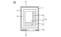
- FIG. 1 is a plan view of a hollow package according to Embodiment 1.
- FIG. FIG. 2 is a cross-sectional view obtained by cutting FIG. 1 along the line AB.
- 1 is a plan view of a device substrate according to Embodiment 1.
- FIG. 2 is a cross-sectional view obtained by cutting FIG. 1 along the line CD.
- FIG. 3 is a bottom view of the lid substrate according to the first embodiment.
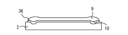
- FIG. 6 is a cross-sectional view obtained by cutting FIG. 5 along the line EF.
- 3 is a diagram showing the shape of a sealing ring according to Embodiment 1.
- FIG. FIG. 7 is a diagram showing the shape of a sealing ring according to a modification of the first embodiment.
- FIG. 7 is a diagram showing the shape of a sealing ring according to a modification of the first embodiment.
- FIG. 7 is a diagram showing the shape of a sealing ring according to a modification of the first embodiment.
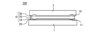
- FIG. 3 is a plan view of a hollow package according to a second embodiment. 12 is a cross-sectional view obtained by cutting FIG. 11 along the line AB.
- FIG. 3 is a plan view of a device substrate according to a second embodiment. 4 is a cross-sectional view obtained by cutting FIG. 3 along the line CD.
- FIG. FIG. 7 is a plan view of a hollow package according to Embodiment 3; 16 is a cross-sectional view obtained by cutting FIG. 15 along the line AB.
- FIG. 7 is a bottom view of a lid substrate according to Embodiment 3;
- FIG. 1 is a plan view of a hollow package 100 according to the first embodiment.
- FIG. 2 is a cross-sectional view obtained by cutting FIG. 1 along the line AB.
- the hollow package 100 includes a device substrate 1 and a lid substrate 2 provided above the device substrate 1.
- the position of the lid substrate 2 is shown by a broken line for convenience.
- a sealing ring 16 is provided on the upper surface of the device substrate 1.
- a sealing ring 36 is provided on the lower surface of the lid substrate 2 facing the device substrate 1 so as to face the sealing ring 16 .
- Seal layer 26 joins sealing ring 16 and sealing ring 36.
- the sealing rings 16 and 36 are made of Ni, for example.
- the seal layer 26 is, for example, solder.
- the sealing rings 16, 36 and the seal layer 26 are collectively referred to as a seal 6.
- the device substrate 1 and the lid substrate 2 are bonded to each other by a seal 6.
- the sealing rings 16 and 36 are intermediate layers for bonding the device substrate 1, the lid substrate 2, and the sealing layer 26.
- the device substrate 1, the lid substrate 2, the sealing rings 16, 36, and the sealing layer 26 form a hollow element structure.
- the hollow package 100 is also called an airtight package.
- Functional elements 3, 4, and 5 are provided in a hollow portion surrounded by the device substrate 1, the lid substrate 2, the sealing rings 16, 36, and the sealing layer 26.
- FIG. 3 is a plan view of the device substrate 1 according to the first embodiment.
- FIG. 4 is a cross-sectional view obtained by cutting FIG. 4 along the straight line CD.
- the functional elements 3, 4, and 5 are collectively referred to as a device 12.
- the device 12 is arranged on the upper surface of the device substrate 1 inside the sealing ring 16 .
- the device 12 includes, for example, MEMS (Micro Electro Mechanical Systems) and a semiconductor device.
- a plurality of bonding pads 14 are arranged outside the sealing ring 16.
- the bonding pad 14 is electrically connected to a wiring board (not shown) or the like.
- the upper surface of the sealing ring 16 has no depressions and is flat.
- FIG. 5 is a bottom view of the lid substrate 2 according to the first embodiment.
- FIG. 6 is a cross-sectional view obtained by cutting FIG. 5 along the line EF. Note that the seal layer 26 is also illustrated in FIG.
- the sealing ring 36 has a corner portion 36a in plan view.
- a recess 10 is formed in a corner 36 a of the sealing ring 36 in a direction perpendicular to the upper surface of the device substrate 1 .
- the recess 10 is formed, for example, at each corner 36a.
- An adsorbent 8 for adsorbing gas may be formed in a portion of the lid substrate 2 surrounded by the sealing ring 36.
- the adsorbent 8 is also called a getter.
- a depression may be formed on the lower surface of the lid substrate 2 in order to increase the hollow volume.
- the hollow package 100 constitutes, for example, a micro electromechanical system (MEMS) device.
- MEMS devices sensors, actuators, etc. are integrated on a device substrate using microfabrication technology.
- the device substrate 1 of this embodiment is, for example, a Si substrate.
- the device substrate 1 may be a compound semiconductor substrate such as GaAs, InP, GaN, or SiC.
- MEMS devices include infrared sensors, gyro sensors, acceleration sensors, etc.
- uncooled infrared sensors are also called thermal sensors.
- Uncooled infrared sensors convert incoming infrared radiation into heat.
- An uncooled infrared sensor reads out changes in the temperature of an object as changes in electrical signals.
- Such an infrared sensor has a heat insulating structure in which the sensor, which is an imaging element, is thermally isolated from the base material in order to increase the detection sensitivity of infrared rays.
- infrared sensors are generally placed in a vacuum environment. In other words, the infrared sensor is placed in a sealed vacuum space.
- the hollow package 100 of this embodiment is, for example, a vacuum package that includes such a sensor.
- solder tends to accumulate at the corners of a sealing ring.
- the solder ends up in a raised shape at the corners of the sealing ring. If such a solder pool is large, there is a risk that the solder will overflow inside the sealing ring during bonding. This may cause the solder to come into contact with a semiconductor circuit or wiring arranged near the sealing ring on the device substrate. This can result in short circuits or broken wiring, which can result in device malfunction.
- a hollow element structure may be formed using a casing.
- manufacturing costs for packaging may increase.
- the bonding material for bonding the device inside the housing needs to be selected from a material that has a higher melting point and produces less gas released than the bonding material for forming the hollow element structure. Therefore, there is a possibility that material costs will increase.
- the recess 10 is formed at the corner 36a of the sealing ring 36.
- solder pooling can be alleviated.
- the solder reflow process melts and flows the solder onto the sealing ring.
- this phenomenon is not limited to the case where the seal layer 26 is made of solder. From the above, when the device substrate 1 and the lid substrate 2 are bonded, solder can be prevented from overflowing inside the sealing ring. Therefore, it is possible to improve reliability and yield. Furthermore, manufacturing costs can be reduced compared to the case where a housing is used for the hollow element structure.
- the recess 10 is formed only at the corner 36a of the sealing ring 36, and the recess 10 is not formed at the straight portion of the sealing ring 36.
- the present invention is not limited to this, and the recess 10 may be formed locally in a portion of the sealing ring 36 that includes the corner 36a. That is, the recess 10 may be formed at the corner 36a of the sealing ring 36 and at a part of the straight portion.
- the recess 10 may be formed in the sealing ring 16 instead of the sealing ring 36.
- the same effect as when the recess 10 is formed in the sealing ring 36 can be obtained.
- the sealing ring 16 or the sealing ring 36 has a corner in a plan view, and a recess is locally formed in a portion including the corner.
- the shape of the recess 10 in plan view is not limited to a circle, but may be an ellipse, a polygon, or the like.
- the cross-sectional shape of the recess 10 is not limited to a U-shape, but may be a V-shape or a polygon.
- FIG. 7 is a diagram showing the shape of the sealing ring according to the first embodiment.
- 8 to 10 are diagrams showing shapes of sealing rings according to modified examples of the first embodiment.
- the sealing rings 16 and 36 of this embodiment are rectangular or square in plan view, as shown in FIG. The present invention is not limited to this, and the sealing rings 16 and 36 may have a polygonal shape such as a pentagon in plan view.
- the sealing rings 16, 36 may be partially recessed in plan view.
- the sealing rings 16, 36 may be partially curved.
- the sealing rings 16 and 36 are formed, for example, by electrolytic Ni plating, and the sealing layer 26 is formed, for example, by lead-free solder.
- the recess 10 is formed by reflecting the shape of the recess formed in the lid substrate 2 on the surface of the sealing ring 36. That is, recesses are locally formed in the lid substrate 2 at portions including the corners.
- the recessed portion of the lid substrate 2 can be formed by existing photolithography technology and Si etching technology before electrolytic Ni plating is formed.
- any width and depth can be selected depending on the pattern size of the photomask.
- any width can be selected depending on the pattern size of the photomask using existing photolithography technology. Further, by adjusting the amount of solder loaded on the sealing ring 36, it is possible to obtain an arbitrary thickness of the seal 6. The width of the sealing rings 16, 36 and the thickness of the seal 6 can be adjusted to obtain any hollow element structure.
- the sealing rings 16 and 36 are made of Ni, and the sealing layer 26 is made of solder. Electrolytic Ni plating and solder are alloyed during bonding. Thereby, the inside and outside of the hollow element structure can be isolated by the seal 6.
- the interior of the hollow element structure is a vacuum atmosphere or a gas atmosphere such as N2. By blocking the inside and outside of the hollow element structure, an airtight package can be constructed that maintains the atmosphere inside the package.
- the sealing rings 16 and 36 are not limited to electroplating, but may be formed by electroless plating, sputtering, MO-CVD (Metal Organic Chemical Vapor Deposition), or the like.
- the width of the sealing rings 16, 36 may be selected not only by photolithography but also by printing, inkjet, mask sputtering, or the like.
- the material of the sealing layer 26 is not limited to lead-free solder, and any material can be selected. However, since high-temperature solder or AuSn has an environmental impact or is expensive, lead-free solder is preferred.
- FIG. 11 is a plan view of a hollow package 200 according to the second embodiment.
- FIG. 12 is a cross-sectional view obtained by cutting FIG. 11 along the line AB.
- FIG. 13 is a plan view of the device substrate 1 according to the second embodiment.
- FIG. 14 is a cross-sectional view obtained by cutting FIG. 3 along the line CD.
- Embodiment 2 differs from Embodiment 1 in that recesses 10 and 11 are formed in both sealing rings 16 and 36 before soldering.
- the sealing ring 16 has a corner 16a in plan view.
- a recess 11 is formed in a corner 16 a of the sealing ring 16 in a direction perpendicular to the upper surface of the device substrate 1 .
- the structure of the lid substrate 2 of this embodiment is similar to the structure of the lid substrate 2 of the first embodiment. Similar to the first embodiment, a recess 10 is formed in the corner 36a of the sealing ring 36.
- a step is formed by the insulating film 20 or the like in the region of the device substrate 1 where the sealing ring 16 is formed.
- the sealing ring 16 is formed on the insulating film 20.
- a recessed portion is formed at a corner of the upper surface of the insulating film 20 .
- the recess 11 is formed by reflecting the shape of the recess formed in the insulating film 20 on the surface of the sealing ring 16. In other words, concave portions are locally formed in the insulating film 20 at portions including corners.
- the recess 11 can absorb the solder mounted on the lid substrate 2 during solder bonding. Therefore, overflowing of solder into the inside of the device substrate 1 can be further suppressed.
- the lid substrate 2 that serves as the lid of the hollow package 200. Therefore, a recess can be formed in the lid substrate 2 itself.
- the device substrate 1 includes wiring and device structures. Therefore, it is preferable to form the recess 11 in the sealing ring 16 by forming the recess in the insulating film 20 or the like instead of the device substrate 1.
- the lid substrate 2 may be provided with wiring or a device structure. In this case, similarly to the device substrate 1, it is preferable to form the recesses in the insulating film or the like rather than in the substrate itself.
- the recess 10 may be formed locally in a portion of the sealing ring 36 that includes the corner 36a, and the recess 11 may be formed locally in a portion of the sealing ring 16 that includes the corner 16a. It is good if it is formed.
- the shape of the recesses 10 and 11 in plan view is not limited to a circle, but may be an ellipse, a polygon, or the like.
- the cross-sectional shape of the recesses 10 and 11 is not limited to a U-shape, but may be a V-shape or a polygon.
- the modified example of the shape of the sealing ring and the method of manufacturing hollow package 100 shown in Embodiment 1 can also be applied to this embodiment.
- FIG. 15 is a plan view of a hollow package 300 according to the third embodiment.
- FIG. 16 is a cross-sectional view obtained by cutting FIG. 15 along the line AB.
- the structure of the sealing ring 36 is different from that in the first embodiment.
- the other configurations are similar to those of the first embodiment.
- FIG. 17 is a bottom view of the lid substrate 2 according to the third embodiment.
- the sealing ring 36 has a corner portion 36a in plan view. The corner portion 36a is wider than the portion of the sealing ring 36 other than the corner portion 36a.
- the sealing ring 36 has a first portion 36b extending in a first direction and a second portion 36c extending in a second direction intersecting the first direction.
- the first direction is the x direction and the second direction is the y direction.
- a corner portion 36a is formed at the intersection of the first portion 36b and the second portion 36c. The corner portion 36a protrudes in the first direction and the second direction.
- solder is more likely to accumulate on the corners of the sealing ring than on the straight portions.
- a wide portion is formed at the corner portion 36a of the sealing ring 36.
- the wide corner portion may be provided on the sealing ring 16 instead of the sealing ring 36. Wide corners may be provided on both sealing rings 16, 36. In this case as well, the same effects as in this embodiment can be obtained.
- the corner portion 36a may protrude only in one of the first direction and the second direction. Although the corner portion 36a in this embodiment is square, it may be circular, oval, polygonal, or the like. Further, the modification of the shape of the sealing ring shown in Embodiment 1 can also be applied to this embodiment. For example, the wide corner portion of this embodiment may be applied to a corner portion where the first portion and the second portion of the sealing ring do not perpendicularly intersect as shown in FIG. 8 .
- the sealing ring 16 or the sealing ring 36 may be made of Ni, and the sealing layer 26 may be made of solder.
- FIG. 18 is a bottom view of the lid substrate 2 according to the fourth embodiment.
- FIG. 19 is a cross-sectional view obtained by cutting FIG. 18 along the line AB.
- the corner 36a of the sealing ring 36 has the recess 10 formed therein, and is wider than the portion other than the corner 36a.
- the width of the corner portion 36a of the sealing ring 36 may be made wider than the width of the portion other than the corner portion 36a.
- the widths of the corners 16a, 36a of the sealing rings 16, 36 may be made wider than the widths of the portions other than the corners.
- the features of the corner portions 16a and 36a described in Embodiments 1 to 3 can be combined arbitrarily.
- the sealing ring 16 may be provided with the recess 11, and the sealing ring 36 may be provided with a wide corner 36a.
Landscapes
- Engineering & Computer Science (AREA)
- Computer Hardware Design (AREA)
- Microelectronics & Electronic Packaging (AREA)
- Solid State Image Pick-Up Elements (AREA)
- Micromachines (AREA)
Priority Applications (4)
| Application Number | Priority Date | Filing Date | Title |
|---|---|---|---|
| CN202280090515.8A CN118900818A (zh) | 2022-04-11 | 2022-04-11 | 中空封装 |
| PCT/JP2022/017500 WO2023199375A1 (ja) | 2022-04-11 | 2022-04-11 | 中空パッケージ |
| US18/718,192 US12550755B2 (en) | 2022-04-11 | 2022-04-11 | Hollow package |
| JP2022547771A JP7231118B1 (ja) | 2022-04-11 | 2022-04-11 | 中空パッケージ |
Applications Claiming Priority (1)
| Application Number | Priority Date | Filing Date | Title |
|---|---|---|---|
| PCT/JP2022/017500 WO2023199375A1 (ja) | 2022-04-11 | 2022-04-11 | 中空パッケージ |
Publications (1)
| Publication Number | Publication Date |
|---|---|
| WO2023199375A1 true WO2023199375A1 (ja) | 2023-10-19 |
Family
ID=85380665
Family Applications (1)
| Application Number | Title | Priority Date | Filing Date |
|---|---|---|---|
| PCT/JP2022/017500 Ceased WO2023199375A1 (ja) | 2022-04-11 | 2022-04-11 | 中空パッケージ |
Country Status (4)
| Country | Link |
|---|---|
| US (1) | US12550755B2 (https=) |
| JP (1) | JP7231118B1 (https=) |
| CN (1) | CN118900818A (https=) |
| WO (1) | WO2023199375A1 (https=) |
Citations (7)
| Publication number | Priority date | Publication date | Assignee | Title |
|---|---|---|---|---|
| JP2006173557A (ja) * | 2004-11-22 | 2006-06-29 | Toshiba Corp | 中空型半導体装置とその製造方法 |
| JP2016531421A (ja) * | 2013-07-11 | 2016-10-06 | レイセオン カンパニー | 真空ゲッタとして使用されるウェファレベルのパッケージされた半田バリア |
| US10314171B1 (en) * | 2017-12-29 | 2019-06-04 | Intel Corporation | Package assembly with hermetic cavity |
| JP2019155566A (ja) * | 2018-03-15 | 2019-09-19 | 新日本無線株式会社 | Mems素子およびその実装構造 |
| JP2020076782A (ja) * | 2020-01-15 | 2020-05-21 | セイコーエプソン株式会社 | 電子デバイス、電子機器、および移動体 |
| JP2020175500A (ja) * | 2019-04-22 | 2020-10-29 | ウーハン イエンシー マイクロ コンポーネンツ カンパニーリミテッド | Memsデバイス及びその製造方法 |
| US20210276859A1 (en) * | 2018-09-26 | 2021-09-09 | Ignite, Inc. | A MEMS Package |
Family Cites Families (8)
| Publication number | Priority date | Publication date | Assignee | Title |
|---|---|---|---|---|
| JP3878897B2 (ja) | 2002-08-30 | 2007-02-07 | 京セラ株式会社 | 半導体素子収納用パッケージおよび半導体装置 |
| JP2008192700A (ja) * | 2007-02-01 | 2008-08-21 | Alps Electric Co Ltd | 電子部品 |
| JP2008218811A (ja) | 2007-03-06 | 2008-09-18 | Hitachi Metals Ltd | 機能素子パッケージ |
| JP2010161271A (ja) * | 2009-01-09 | 2010-07-22 | Panasonic Corp | 半導体パッケージ |
| TWI429570B (zh) * | 2012-03-23 | 2014-03-11 | Gudeng Prec Ind Co Ltd | 具有扣合結構之光罩盒 |
| JP2015170685A (ja) | 2014-03-06 | 2015-09-28 | 三菱電機株式会社 | 基板装置 |
| JP2019153849A (ja) * | 2018-02-28 | 2019-09-12 | セイコーエプソン株式会社 | 発振器、電子機器および移動体 |
| TWI687760B (zh) * | 2019-04-16 | 2020-03-11 | 家登精密工業股份有限公司 | 具有擾流結構的光罩盒 |
-
2022
- 2022-04-11 US US18/718,192 patent/US12550755B2/en active Active
- 2022-04-11 CN CN202280090515.8A patent/CN118900818A/zh active Pending
- 2022-04-11 JP JP2022547771A patent/JP7231118B1/ja active Active
- 2022-04-11 WO PCT/JP2022/017500 patent/WO2023199375A1/ja not_active Ceased
Patent Citations (7)
| Publication number | Priority date | Publication date | Assignee | Title |
|---|---|---|---|---|
| JP2006173557A (ja) * | 2004-11-22 | 2006-06-29 | Toshiba Corp | 中空型半導体装置とその製造方法 |
| JP2016531421A (ja) * | 2013-07-11 | 2016-10-06 | レイセオン カンパニー | 真空ゲッタとして使用されるウェファレベルのパッケージされた半田バリア |
| US10314171B1 (en) * | 2017-12-29 | 2019-06-04 | Intel Corporation | Package assembly with hermetic cavity |
| JP2019155566A (ja) * | 2018-03-15 | 2019-09-19 | 新日本無線株式会社 | Mems素子およびその実装構造 |
| US20210276859A1 (en) * | 2018-09-26 | 2021-09-09 | Ignite, Inc. | A MEMS Package |
| JP2020175500A (ja) * | 2019-04-22 | 2020-10-29 | ウーハン イエンシー マイクロ コンポーネンツ カンパニーリミテッド | Memsデバイス及びその製造方法 |
| JP2020076782A (ja) * | 2020-01-15 | 2020-05-21 | セイコーエプソン株式会社 | 電子デバイス、電子機器、および移動体 |
Also Published As
| Publication number | Publication date |
|---|---|
| US12550755B2 (en) | 2026-02-10 |
| JP7231118B1 (ja) | 2023-03-01 |
| US20250046746A1 (en) | 2025-02-06 |
| JPWO2023199375A1 (https=) | 2023-10-19 |
| CN118900818A (zh) | 2024-11-05 |
Similar Documents
| Publication | Publication Date | Title |
|---|---|---|
| KR101931010B1 (ko) | 응력 감소층을 갖는 기밀 밀봉된 패키지 | |
| US7485956B2 (en) | Microelectronic package optionally having differing cover and device thermal expansivities | |
| US20110115036A1 (en) | Device packages and methods of fabricating the same | |
| KR101043644B1 (ko) | 접합용 구조물 및 이를 이용한 기판 접합 방법 | |
| JP5537306B2 (ja) | 電子部品収納用パッケージ、および電子装置 | |
| KR101048085B1 (ko) | 기능성 소자 패키지 및 그 제조 방법 | |
| JP2022125097A (ja) | 圧電振動デバイス | |
| US7262498B2 (en) | Assembly with a ring and bonding pads formed of a same material on a substrate | |
| WO2023199375A1 (ja) | 中空パッケージ | |
| US7919842B2 (en) | Structure and method for sealing cavity of micro-electro-mechanical device | |
| CN101421178A (zh) | 用于制造电子组件的方法、电子组件、覆盖物和衬底 | |
| US7524704B2 (en) | Method for encapsulating a component, especially an electric or electronic component, by means of an improved solder seam | |
| JP7605334B2 (ja) | 気密パッケージ素子および素子モジュール | |
| CN101490955A (zh) | 框架及制造组件的方法 | |
| KR20050116760A (ko) | 이미지 센서용 패키지 | |
| JP7542738B2 (ja) | 気密パッケージ素子および素子モジュール | |
| JP2011500343A (ja) | 多層バンプ構造物及びその製造方法 | |
| KR102610614B1 (ko) | 허메틱 실링 패키지 모듈 및 그 제조 방법 | |
| JP2009038285A (ja) | 封止構造体 | |
| JP2012253117A (ja) | 半導体装置 | |
| KR100941446B1 (ko) | 복층 범프 구조물 및 그 제조 방법 | |
| KR101043643B1 (ko) | 접합용 구조물 및 이를 이용한 기판 접합 방법 | |
| JP5768665B2 (ja) | 半導体パッケージおよびその製造方法。 | |
| TWI605010B (zh) | 微機電系統封裝結構及其製作方法 | |
| JP5791263B2 (ja) | 電子部品収納用パッケージおよび実装構造体 |
Legal Events
| Date | Code | Title | Description |
|---|---|---|---|
| WWE | Wipo information: entry into national phase |
Ref document number: 2022547771 Country of ref document: JP |
|
| 121 | Ep: the epo has been informed by wipo that ep was designated in this application |
Ref document number: 22937355 Country of ref document: EP Kind code of ref document: A1 |
|
| WWE | Wipo information: entry into national phase |
Ref document number: 18718192 Country of ref document: US |
|
| WWE | Wipo information: entry into national phase |
Ref document number: 202280090515.8 Country of ref document: CN |
|
| NENP | Non-entry into the national phase |
Ref country code: DE |
|
| 122 | Ep: pct application non-entry in european phase |
Ref document number: 22937355 Country of ref document: EP Kind code of ref document: A1 |
|
| WWG | Wipo information: grant in national office |
Ref document number: 18718192 Country of ref document: US |