WO2023189419A1 - 電気接点材料、ならびにこれを用いた接点、端子およびコネクタ - Google Patents
電気接点材料、ならびにこれを用いた接点、端子およびコネクタ Download PDFInfo
- Publication number
- WO2023189419A1 WO2023189419A1 PCT/JP2023/009300 JP2023009300W WO2023189419A1 WO 2023189419 A1 WO2023189419 A1 WO 2023189419A1 JP 2023009300 W JP2023009300 W JP 2023009300W WO 2023189419 A1 WO2023189419 A1 WO 2023189419A1
- Authority
- WO
- WIPO (PCT)
- Prior art keywords
- silver
- electrical contact
- containing layer
- layer
- contact material
- Prior art date
- Legal status (The legal status is an assumption and is not a legal conclusion. Google has not performed a legal analysis and makes no representation as to the accuracy of the status listed.)
- Ceased
Links
Images
Classifications
-
- H—ELECTRICITY
- H01—ELECTRIC ELEMENTS
- H01R—ELECTRICALLY-CONDUCTIVE CONNECTIONS; STRUCTURAL ASSOCIATIONS OF A PLURALITY OF MUTUALLY-INSULATED ELECTRICAL CONNECTING ELEMENTS; COUPLING DEVICES; CURRENT COLLECTORS
- H01R13/00—Details of coupling devices of the kinds covered by groups H01R12/70 or H01R24/00 - H01R33/00
- H01R13/02—Contact members
- H01R13/03—Contact members characterised by the material, e.g. plating, or coating materials
-
- H—ELECTRICITY
- H01—ELECTRIC ELEMENTS
- H01B—CABLES; CONDUCTORS; INSULATORS; SELECTION OF MATERIALS FOR THEIR CONDUCTIVE, INSULATING OR DIELECTRIC PROPERTIES
- H01B1/00—Conductors or conductive bodies characterised by the conductive materials; Selection of materials as conductors
- H01B1/02—Conductors or conductive bodies characterised by the conductive materials; Selection of materials as conductors mainly consisting of metals or alloys
-
- C—CHEMISTRY; METALLURGY
- C22—METALLURGY; FERROUS OR NON-FERROUS ALLOYS; TREATMENT OF ALLOYS OR NON-FERROUS METALS
- C22C—ALLOYS
- C22C5/00—Alloys based on noble metals
- C22C5/06—Alloys based on silver
-
- C—CHEMISTRY; METALLURGY
- C23—COATING METALLIC MATERIAL; COATING MATERIAL WITH METALLIC MATERIAL; CHEMICAL SURFACE TREATMENT; DIFFUSION TREATMENT OF METALLIC MATERIAL; COATING BY VACUUM EVAPORATION, BY SPUTTERING, BY ION IMPLANTATION OR BY CHEMICAL VAPOUR DEPOSITION, IN GENERAL; INHIBITING CORROSION OF METALLIC MATERIAL OR INCRUSTATION IN GENERAL
- C23C—COATING METALLIC MATERIAL; COATING MATERIAL WITH METALLIC MATERIAL; SURFACE TREATMENT OF METALLIC MATERIAL BY DIFFUSION INTO THE SURFACE, BY CHEMICAL CONVERSION OR SUBSTITUTION; COATING BY VACUUM EVAPORATION, BY SPUTTERING, BY ION IMPLANTATION OR BY CHEMICAL VAPOUR DEPOSITION, IN GENERAL
- C23C28/00—Coating for obtaining at least two superposed coatings either by methods not provided for in a single one of groups C23C2/00 - C23C26/00 or by combinations of methods provided for in subclasses C23C and C25C or C25D
- C23C28/02—Coating for obtaining at least two superposed coatings either by methods not provided for in a single one of groups C23C2/00 - C23C26/00 or by combinations of methods provided for in subclasses C23C and C25C or C25D only coatings only including layers of metallic material
- C23C28/021—Coating for obtaining at least two superposed coatings either by methods not provided for in a single one of groups C23C2/00 - C23C26/00 or by combinations of methods provided for in subclasses C23C and C25C or C25D only coatings only including layers of metallic material including at least one metal alloy layer
-
- C—CHEMISTRY; METALLURGY
- C23—COATING METALLIC MATERIAL; COATING MATERIAL WITH METALLIC MATERIAL; CHEMICAL SURFACE TREATMENT; DIFFUSION TREATMENT OF METALLIC MATERIAL; COATING BY VACUUM EVAPORATION, BY SPUTTERING, BY ION IMPLANTATION OR BY CHEMICAL VAPOUR DEPOSITION, IN GENERAL; INHIBITING CORROSION OF METALLIC MATERIAL OR INCRUSTATION IN GENERAL
- C23C—COATING METALLIC MATERIAL; COATING MATERIAL WITH METALLIC MATERIAL; SURFACE TREATMENT OF METALLIC MATERIAL BY DIFFUSION INTO THE SURFACE, BY CHEMICAL CONVERSION OR SUBSTITUTION; COATING BY VACUUM EVAPORATION, BY SPUTTERING, BY ION IMPLANTATION OR BY CHEMICAL VAPOUR DEPOSITION, IN GENERAL
- C23C28/00—Coating for obtaining at least two superposed coatings either by methods not provided for in a single one of groups C23C2/00 - C23C26/00 or by combinations of methods provided for in subclasses C23C and C25C or C25D
- C23C28/02—Coating for obtaining at least two superposed coatings either by methods not provided for in a single one of groups C23C2/00 - C23C26/00 or by combinations of methods provided for in subclasses C23C and C25C or C25D only coatings only including layers of metallic material
- C23C28/023—Coating for obtaining at least two superposed coatings either by methods not provided for in a single one of groups C23C2/00 - C23C26/00 or by combinations of methods provided for in subclasses C23C and C25C or C25D only coatings only including layers of metallic material only coatings of metal elements only
-
- C—CHEMISTRY; METALLURGY
- C23—COATING METALLIC MATERIAL; COATING MATERIAL WITH METALLIC MATERIAL; CHEMICAL SURFACE TREATMENT; DIFFUSION TREATMENT OF METALLIC MATERIAL; COATING BY VACUUM EVAPORATION, BY SPUTTERING, BY ION IMPLANTATION OR BY CHEMICAL VAPOUR DEPOSITION, IN GENERAL; INHIBITING CORROSION OF METALLIC MATERIAL OR INCRUSTATION IN GENERAL
- C23C—COATING METALLIC MATERIAL; COATING MATERIAL WITH METALLIC MATERIAL; SURFACE TREATMENT OF METALLIC MATERIAL BY DIFFUSION INTO THE SURFACE, BY CHEMICAL CONVERSION OR SUBSTITUTION; COATING BY VACUUM EVAPORATION, BY SPUTTERING, BY ION IMPLANTATION OR BY CHEMICAL VAPOUR DEPOSITION, IN GENERAL
- C23C30/00—Coating with metallic material characterised only by the composition of the metallic material, i.e. not characterised by the coating process
-
- C—CHEMISTRY; METALLURGY
- C25—ELECTROLYTIC OR ELECTROPHORETIC PROCESSES; APPARATUS THEREFOR
- C25D—PROCESSES FOR THE ELECTROLYTIC OR ELECTROPHORETIC PRODUCTION OF COATINGS; ELECTROFORMING; APPARATUS THEREFOR
- C25D5/00—Electroplating characterised by the process; Pretreatment or after-treatment of workpieces
- C25D5/10—Electroplating with more than one layer of the same or of different metals
- C25D5/12—Electroplating with more than one layer of the same or of different metals at least one layer being of nickel or chromium
-
- C—CHEMISTRY; METALLURGY
- C25—ELECTROLYTIC OR ELECTROPHORETIC PROCESSES; APPARATUS THEREFOR
- C25D—PROCESSES FOR THE ELECTROLYTIC OR ELECTROPHORETIC PRODUCTION OF COATINGS; ELECTROFORMING; APPARATUS THEREFOR
- C25D5/00—Electroplating characterised by the process; Pretreatment or after-treatment of workpieces
- C25D5/48—After-treatment of electroplated surfaces
- C25D5/50—After-treatment of electroplated surfaces by heat-treatment
-
- C—CHEMISTRY; METALLURGY
- C25—ELECTROLYTIC OR ELECTROPHORETIC PROCESSES; APPARATUS THEREFOR
- C25D—PROCESSES FOR THE ELECTROLYTIC OR ELECTROPHORETIC PRODUCTION OF COATINGS; ELECTROFORMING; APPARATUS THEREFOR
- C25D7/00—Electroplating characterised by the article coated
Definitions
- the present disclosure relates to electrical contact materials, and contacts, terminals, and connectors using the same.
- Patent Document 1 discloses that the surface of a base material made of copper or copper alloy is coated with a silver plating layer, and the silver plating layer is separated from the first silver plating layer on the lower layer side and the first silver plating layer.
- a silver-plated terminal for a connector is described, which is composed of a second silver-plated layer above a silver-plated layer, and in which the crystal grain size of the first silver-plated layer is larger than the crystal grain size of the second silver-plated layer.
- Patent Document 1 discloses that, regarding silver-plated materials, the crystal grain size of the silver-plated layer tends to increase due to recrystallization, and this increase in crystal grain size lowers hardness and reduces wear resistance.
- the crystal grain size of the silver plating layer is specified as a material with good wear resistance. However, the size of the crystal grains depends on the thickness of the plating layer. Therefore, in order to obtain good wear resistance in Patent Document 1, there is a restriction on the thickness of the silver plating layer.
- Patent Document 2 in a silver plating solution containing silver, potassium cyanide, and selenium at a predetermined concentration, y and x are A method for producing a silver-plated material in which a silver plating film with a purity of 99.9% by mass or more is formed on a base material by electroplating so that a predetermined relationship is achieved.
- Patent Document 2 exemplifies a method for manufacturing a silver-plated material that suppresses an increase in contact resistance while maintaining high hardness by containing elements such as selenium in the silver-plated film, and Vickers hardness is the basis for wear resistance. In this manner, in Patent Document 2, the Vickers hardness of the silver-plated material, which depends on the characteristics of the base material, is used to evaluate the wear resistance. However, it is originally necessary to evaluate the wear resistance of the plating film itself, which is not easily affected by the characteristics of the base material.
- An object of the present disclosure is to provide an electrical contact material with excellent wear resistance that is not easily affected by base material properties, and contacts, terminals, and connectors using the same.
- An electrical contact material comprising an electrically conductive base material and a silver-containing layer containing silver provided on at least a part of the surface of the electrically conductive base material, wherein the silver-containing layer is provided in a cross section of the electrical contact material.
- the silver-containing layer according to [1] or [2] above contains one or more elements selected from the group consisting of Sn, Zn, In, Ni, Cu, Se, Sb and Co. Electrical contact materials.
- an electrical contact material having excellent wear resistance that is not easily affected by base material properties, and contacts, terminals, and connectors using the same.
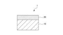
- FIG. 1 is a cross-sectional view showing an example of an electrical contact material according to an embodiment.
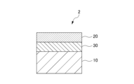
- FIG. 2 is a sectional view showing another example of the electrical contact material of the embodiment.
- the present inventors focused on the amount of strain in the silver-containing layer provided on at least a portion of the surface of the conductive base material, and by controlling the CI value of the silver-containing layer, The inventors have discovered that the wear resistance of contact materials is excellent regardless of the characteristics of the conductive base material, and have completed the present disclosure based on this knowledge.
- the electrical contact material of the embodiment includes an electrically conductive base material and a silver-containing layer containing silver provided on at least a portion of the surface of the electrically conductive base material, and in a cross section of the electrical contact material, the silver-containing layer
- the average CI value of is 0.6 or more.
- FIG. 1 is a cross-sectional view showing an example of an electrical contact material according to an embodiment.
- the electrical contact material 1 includes a conductive base material 10 and a silver-containing layer 20.
- the conductive base material 10 constituting the electrical contact material 1 is a rolled material that has conductivity and is obtained by rolling.
- the conductive base material 10 is made of a copper-based material containing pure copper and a copper alloy, or an iron-based material containing pure iron and an iron alloy.
- it is made of a material.
- Cu-Zn based, Cu-Ni-Si based, Cu-Sn-Ni based, Cu-Cr-Mg based, and Cu-Ni-Si-Zn-Sn-Mg based copper alloys are preferred. .
- the electrical conductivity of the conductive base material 10 is preferably 60% IACS or more, more preferably 80% IACS or more. When the electrical conductivity of the conductive base material 10 is 60% IACS or more, the electrical contact material 1 has good electrical conductivity.
- the shape of the conductive base material 10 may be appropriately selected depending on the use of the electrical contact material 1, but it is preferably strip-shaped, plate-shaped, rod-shaped, or linear.
- the silver-containing layer 20 constituting the electrical contact material 1 is provided on at least a portion of the surface of the conductive base material 10 and contains silver.
- the silver-containing layer 20 covering the surface of the conductive substrate 10 is made of pure silver or a silver alloy, preferably a silver alloy, that is, the silver-containing layer 20 is preferably a silver alloy layer. From the viewpoint that the electrical contact material 1 has excellent abrasion resistance and the abrasion resistance of the electrical contact material 1 is not easily influenced by the characteristics of the conductive base material 10, the silver-containing layer 20 is formed by plating, i.e. It is preferable that the silver-containing layer 20 is a plating film.
- the average CI value of the silver-containing layer 20 is 0.6 or more.
- the cross section of the electrical contact material 1 is a cross section parallel to the rolling direction of the conductive base material 10.
- the second element dissolves in solid solution in the silver crystals in the silver-containing layer 20, improving crystallinity and increasing the coefficient of dynamic friction. Since the hardness is low and high hardness can be maintained, wear resistance can be improved. The higher the average CI value, the higher the reliability of the crystal orientation. From this point of view, the average CI value of the silver-containing layer 20 in the cross section of the electrical contact material 1 is 0.6 or more, and the higher the CI value, the more preferable.
- the average IQ value of the silver-containing layer 20 is preferably 1000 or more, more preferably 1500 or more.
- the crystal quality is good.
- the average IQ value of the silver-containing layer 20 is preferably 2100 or less, more preferably 2000 or less.
- the average IQ value of the silver-containing layer 20 is 2100 or less, the crystal lattice is sufficiently distorted and the strain increases, so that wear resistance can be improved.
- the CI (Confidence Index) value is a value used to index patterns, an index for evaluating whether the calculated crystal orientation is correct, and a value used for evaluating whether the calculated crystal orientation is correct.
- the CI value is a value that reflects the reliability of the crystal orientation within the silver-containing layer 20.
- the IQ (Image Quality) value is a value obtained by plotting the peak intensity indicating a band in the Hough space when the EBSD pattern is Hough-transformed, and its size indicates the good crystallinity in the silver-containing layer 20. , is a value that reflects the amount of distortion.
- CI values and IQ values were measured continuously using an EBSD detector (manufactured by TSL Solutions, OIM5.0 HIKARI) attached to a high-resolution scanning analytical electron microscope (manufactured by JEOL Ltd., JSM-7001FA). It can be obtained from crystal orientation analysis data calculated from orientation data using analysis software (OIM Analysis, manufactured by TSL Solutions).
- the object to be measured is the surface of the silver-containing layer 20 on the cross section of the electrical contact material 1 parallel to the rolling direction of the conductive base material 10, which has been mirror-finished using a cross-section polisher (manufactured by JEOL Ltd.), and the measurement magnification is 30,000. It's double.
- Measurement is performed in steps with a measurement interval of 50 nm or less, excluding measurement points whose CI value analyzed by analysis software is 0.1 or less (noise removal), and where the orientation difference between adjacent pixels is 5.00° or more.
- the boundaries are regarded as grain boundaries, and the CI value and IQ value of the silver-containing layer 20 are obtained.
- the average CI value and average IQ value of the silver-containing layer 20 can be obtained by performing this measurement multiple times (in multiple different measurement regions of the same sample) and calculating the average value.
- the average CI value and the average IQ value are the average values of the CI value and the IQ value in the measurement area of the silver-containing layer measured at a magnification of 30,000 times.
- the silver-containing layer 20 preferably contains one or more elements (hereinafter also referred to as a second element) selected from the group consisting of Sn, Zn, In, Ni, Cu, Se, Sb, and Co.
- a second element selected from the group consisting of Sn, Zn, In, Ni, Cu, Se, Sb, and Co.
- the silver-containing layer 20 is made of one or more types selected from the group consisting of Sn, Zn, In, Ni, Cu, Se, Sb, and Co.
- the total content of the elements is less than 15.0 at%.
- the silver-containing layer 20 is selected from the group consisting of Sn, Zn, In, Ni, Cu, Se, Sb, and Co. It is preferable that the total content of one or more elements is 0.1 at% or more.
- the lower limit of the average thickness of the silver-containing layer 20 is preferably 0.5 ⁇ m or more, more preferably 2.0 ⁇ m or more, and still more preferably 3.0 ⁇ m or more.
- the upper limit of the average thickness of the silver-containing layer 20 is preferably 5.0 ⁇ m or less.
- the lower limit of the average thickness of the silver-containing layer 20 is 0.5 ⁇ m or more, the excellent wear resistance of the electrical contact material 1 can be maintained for a long period of time.
- the upper limit of the average thickness of the silver-containing layer 20 is 5.0 ⁇ m or less, material costs can be suppressed.
- FIG. 2 is a sectional view showing another example of the electrical contact material of the embodiment.
- the electrical contact material 2 shown in FIG. 2 has basically the same structure as the electrical contact material 1 shown in FIG. 1 except that the structure of the intermediate layer 30 is added.
- the electrical contact material 2 further includes an intermediate layer 30 made of nickel or a nickel alloy between the conductive base material 10 and the silver-containing layer 20.
- an intermediate layer 30 made of nickel or a nickel alloy between the conductive base material 10 and the silver-containing layer 20.
- the intermediate layer 30 is provided between the surface of the conductive base material 10 and the silver-containing layer 20, thermal diffusion of elements constituting the conductive base material 10 into the silver-containing layer 20 is suppressed, and the conductive base material The adhesion between the silver-containing layer 10 and the silver-containing layer 20 can be improved.
- the intermediate layer 30 is preferably made of pure nickel or a Ni-P-based nickel alloy.
- the lower limit of the average thickness of the intermediate layer 30 is preferably 0.01 ⁇ m or more, more preferably 0.10 ⁇ m or more, and still more preferably 0.30 ⁇ m or more.
- the upper limit of the average thickness of the intermediate layer 30 is preferably 3.00 ⁇ m or less, more preferably 2.00 ⁇ m or less, and still more preferably 1.00 ⁇ m or less. If the lower limit of the average thickness of the intermediate layer 30 is less than 0.01 ⁇ m, the above-mentioned suppression of thermal diffusion and improvement of adhesion cannot be achieved. If the upper limit of the average thickness of the intermediate layer 30 is more than 3.00 ⁇ m, bending workability deteriorates. When an electrical contact material is used in a terminal, bending workability of R/t ⁇ 1 is required.
- the electrical contact materials 1 and 2 described above may further include a copper layer (not shown) directly below the silver-containing layer 20, which is the surface layer.
- the copper layer (not shown) is made of pure copper or a copper alloy.
- the thickness of the copper layer (not shown) is significantly smaller than the thickness of the conductive base material 10.
- the electrical contact materials 1 and 2 have excellent abrasion resistance that is not easily affected by the characteristics of the conductive base material 10, so the electrical contact materials 1 and 2 are suitable for contacts, terminals, and connectors. Can be used. These contacts are contacts made using electrical contact materials 1 and 2, terminals are terminals made using electrical contact materials 1 and 2, and connectors are made using electrical contact materials 1 and 2. This is a connector made using
- a silver-containing layer is formed on at least a portion of the surface of a conductive base material by a plating method or the like. Subsequently, the base material provided with the silver-containing layer on the surface is rolled. In this way, the electrical contact material 1 can be manufactured.
- an intermediate layer is formed on at least a portion of the surface of the conductive base material by a plating method or the like.
- a silver-containing layer is formed on the intermediate layer by a plating method or the like.
- the substrate comprising the intermediate layer and the silver-containing layer is rolled. In this way, the electrical contact material 2 can be manufactured.
- the plating conditions for the silver-containing layer by setting the current density to 5 A/dm 2 or more and 10 A/dm 2 or less and the bath temperature (liquid temperature) to 25°C or more to prioritize nucleation, crystal grains with different crystal orientations can be formed. Since the silver-containing layer grows in large numbers and the difference in crystal orientation increases, the internal stress of the silver-containing layer can be further increased. By controlling the current density and temperature within the above range, the amount of strain in the silver-containing layer can be controlled. Even if the temperature is 25°C or higher, if the current density is less than 5 A/ dm2 , the crystal grains will become coarse, the number of crystal grains with different crystal orientations will decrease, and the amount of strain in the silver-containing layer will decrease.
- the lower limit is 20% or more, preferably 25% or more, and the upper limit is 30% or less.
- the processing rate is 20% or more, the amount of strain in the silver-containing layer can be increased and wear resistance can be improved.
- the processing rate is 30% or less, deterioration in bending workability due to excessive strain in the silver-containing layer can be suppressed.
- the processing rate of rolling is a percentage obtained by dividing the difference between the cross-sectional area of the sample before rolling and the cross-sectional area of the sample after rolling by the cross-sectional area of the sample before rolling.
- heat treatment is performed at 300° C. or higher and 600° C. or lower for 5 seconds or more and 60 seconds or less.
- the strain introduced by plating can be made uniform.
- the strain within the crystal grains is released, thereby making it possible to control the average CI value of the silver-containing layer to 0.6 or more.
- the strain within the crystal grains is released, thereby making it possible to control the average CI value of the silver-containing layer to 0.6 or more.
- crystallinity improves. As a result, control of the CI value and IQ value within a predetermined range is improved.
- the heat treatment temperature is less than 300°C or the heat treatment time is less than 5 seconds, the strain within the crystal grains cannot be sufficiently released and the strain cannot be concentrated near the grain boundaries, so the average CI value will be 0. It becomes less than .6.
- the heat treatment temperature exceeds 600°C and/or the heat treatment time exceeds 60 seconds, the average CI value will similarly exceed 0.6, and the material strength will decrease due to excessive heat treatment, causing contact , cannot maintain sufficient strength when used in terminals and connectors.
- a plating method using a plating bath containing the silver-containing component and the second element component is used.
- a silver-containing layer containing two elements may be directly formed.
- a silver-containing layer containing a second element may be formed by alternately forming a silver-containing layer and a second element layer by plating or the like, and then performing heat treatment. good.
- the processing rate of the rolling process is preferably 20% or more and 30% or less from the same viewpoint as above.
- the heat treatment in this case may be replaced by a heat treatment performed after forming the above-described silver-containing layer and before rolling.
- Examples 1-2, 17 The base material (manufactured by Furukawa Electric, EFTEC-550T, 80% IACS) was electrolytically degreased and then acid washed. Thereafter, a silver-containing layer was formed on the substrate surface by plating (current density 10 A/dm 2 ) in an alkali cyanide silver bath (silver cyanide 50 g/L, potassium cyanide 100 g/L) at a bath temperature of 25°C, and then Heat treatment was performed at 300° C. or higher and 600° C. or lower for 5 seconds or more and 60 seconds or less. Subsequently, electrical contact materials having the silver-containing layer (pure silver layer) shown in Table 1 were manufactured by rolling at the processing rate shown in Table 1.
- Examples 3, 10, 11, 18, 25, 26 The base material (manufactured by Furukawa Electric, EFTEC-550T, 80% IACS) was electrolytically degreased and then acid washed. Thereafter, a silver-containing layer was formed on the substrate surface by plating (current density 10 A/dm 2 ) in an alkali cyanide silver bath (silver cyanide 50 g/L, potassium cyanide 100 g/L) at a bath temperature of 25°C, and then A tin layer is formed by plating method (current density 10 A/dm 2 ) in a sulfuric acid bath (tin sulfate 80 g/L, sulfuric acid 80 g/L) at a bath temperature of 25°C, and then heated at 300°C or higher and 600°C or lower for 5 seconds or more. Heat treatment was performed for 60 seconds or less. Subsequently, electrical contact materials having the silver-containing layer (silver alloy layer) shown in Table 1 were manufactured by rolling at the processing rate
- Example 4 The base material (manufactured by Furukawa Electric, EFTEC-550T, 80% IACS) was electrolytically degreased and then acid washed. After that, alkali cyanide silver bath (silver cyanide 50-100 g/L, potassium cyanide 100-200 g/L, zinc chloride 10 g/L (Example 4), copper chloride dihydrate 12 g/L (example 4), bath temperature 25 ° C. Example 7), 10 g/L of nickel chloride (Example 29)) was used to form a silver-containing layer containing a second element on the surface of the substrate by plating (current density 5 to 10 A/dm 2 ), and then heated to 300°C. Heat treatment was performed at 600° C. or higher for 5 seconds or more and 60 seconds. Subsequently, electrical contact materials having the silver-containing layer (silver alloy layer) shown in Table 1 were manufactured by rolling at the processing rate shown in Table 1.
- Example 5 The base material (manufactured by Furukawa Electric, EFTEC-550T, 80% IACS) was electrolytically degreased and then acid washed. Thereafter, the intermediate layer was plated using a plating method (current density 10 A/dm 2 ) in a nickel plating bath (nickel sulfate hexahydrate 500 g/L, nickel chloride 30 g/L, boric acid 30 g/L) at a bath temperature of 55°C.
- a plating method current density 10 A/dm 2
- nickel plating bath nickel sulfate hexahydrate 500 g/L, nickel chloride 30 g/L, boric acid 30 g/L
- an alkali cyanide silver bath (silver cyanide 50-100 g/L, potassium cyanide 100-200 g/L, indium trichloride 15 g/L) at a bath temperature of 25°C to form a silver-containing layer containing a second element.
- a layer was formed on the surface of the intermediate layer by a plating method (current density 5 to 10 A/dm 2 ), followed by heat treatment at 300° C. to 600° C. for 5 seconds to 60 seconds. Subsequently, rolling was performed at the processing rates shown in Table 1 to produce electrical contact materials having the silver-containing layer (silver alloy layer) and intermediate layer (pure nickel layer) shown in Table 1.
- a nickel plating bath (nickel sulfate hexahydrate 500 g/L, nickel chloride 30 g/L, boric acid 30 g/L) at a bath temperature of 55°C (Comparative Examples 2, 5-6, 10, 13-14, 18, 21-22, 26, 29-30, 34, 38, 42, 46, 50, 54, 58, 62) or a nickel-phosphorous electrolytic bath with a bath temperature of 55°C (nickel sulfate hexahydrate 500g/L, chloride Nickel hexahydrate 30g/L, boric acid 30g/L, phosphorous acid 16g/L) (Comparative Examples 4, 7-8, 12, 15-16, 20, 23-24, 28, 31-32, 36 , 39-40, 43, 47-48, 52, 56, 60, 64), an intermediate layer was formed on the surface of the substrate by plating (current density 15 A/dm 2 ), and then an alkali layer was formed at a bath temperature of 25°C.
- Cyanide silver bath (silver cyanide 50-100g/L, potassium cyanide 100-200g/L, zinc chloride 10g/L (Comparative Examples 2, 10, 18, 26, 34, 43, 52, 60), nickel chloride 10g/L (Comparative Examples 4, 12, 20, 28, 36, 46, 54, 62), copper chloride dihydrate 12 g/L (Comparative Examples 5, 13, 21, 29, 38, 47), potassium selenocyanate 2.
- Example 14 The base material (manufactured by Furukawa Electric, EFTEC-550T, 80% IACS) was electrolytically degreased and then acid washed. Thereafter, a silver-containing layer containing a second element was formed by plating (current It was formed on the surface of the substrate at a density of 5 to 10 A/dm 2 ), and then heated at 300° C. to 600° C. for 5 seconds to 60 seconds. Subsequently, electrical contact materials having the silver-containing layer (silver alloy layer) shown in Table 1 were manufactured by rolling at the processing rate shown in Table 1.
- Example 19 The base material (manufactured by Furukawa Electric, EFTEC-550T, 80% IACS) was electrolytically degreased and then acid washed. Thereafter, a silver-containing layer containing a second element was formed by plating (current density 10A) in an alkali cyanide silver bath (silver cyanide 100g/L, potassium cyanide 200g/L, potassium selenocyanate 2.2mg/L) at a bath temperature of 25°C. /dm 2 ) on the surface of the substrate, followed by heat treatment at 300° C. to 600° C. for 5 seconds to 60 seconds. Subsequently, electrical contact materials having the silver-containing layer (silver alloy layer) shown in Table 1 were manufactured by rolling at the processing rate shown in Table 1.
- a silver-containing layer is then formed on the surface of the intermediate layer by plating (current density 10 A/dm 2 ) in an alkali cyanide silver bath (silver cyanide 50 g/L, potassium cyanide 100 g/L) at a bath temperature of 25°C. Then, a tin layer was formed by plating method (current density 10 A/dm 2 ) in a sulfuric acid bath (tin sulfate 80 g/L, sulfuric acid 80 g/L) at a bath temperature of 25°C, and then at a temperature lower than 300°C or Heat treatment was performed at a temperature higher than 600° C. for less than 5 seconds. Subsequently, rolling was carried out at the processing rates shown in Table 2 to produce electrical contact materials having the silver-containing layer (silver alloy layer) and intermediate layer (pure nickel layer) shown in Table 2.
- the surface of the silver-containing layer on the mirror-finished surface of the cross section of the electrical contact material parallel to the rolling direction of the conductive base material was obtained as the measurement target.
- the measurement magnification was 30,000 times. Measurement is performed in steps with a measurement interval of 50 nm or less, excluding measurement points with a CI value of 0.1 or less analyzed by analysis software, and boundaries where the orientation difference between adjacent pixels is 5.00° or more are defined as crystal grains.
- the CI value and IQ value of the silver-containing layer were obtained. This measurement was performed five times (in five different measurement areas of the same sample), and the average value was calculated to obtain the average CI value and average IQ value of the silver-containing layer.
- Dynamic friction coefficient is less than 0.3 ⁇ : Dynamic friction coefficient is 0.3 or more and less than 0.5 ⁇ : Dynamic friction coefficient is 0.5 or more
- Abrasion resistance The surface of the electrical contact material on the silver-containing layer side was tested using a friction and wear tester Tribogear (surface property measuring device TYPE: 14FW, manufactured by Shinto Kagaku Co., Ltd.) under a contact load of 4 N. Reciprocating sliding was performed 50 times at a moving distance of 50 mm and a sliding speed of 100 mm/min. Using a laser roughness meter, the ratio of the depth from the reference surface (the surface that was not sliding back and forth) to the thickness of the silver-containing layer was measured. The wear resistance was ranked as follows.
- ⁇ The ratio of the depth from the reference plane to the thickness of the silver-containing layer is less than 1/10.
- ⁇ The ratio of the depth from the reference plane to the thickness of the silver-containing layer is 1/10 or more and less than 1/5.
- ⁇ The ratio of the depth from the reference plane to the thickness of the silver-containing layer is 1/5 or more
- ⁇ Contact resistance value is less than 0.5 m ⁇ ⁇ : Contact resistance value is 0.5 m ⁇ or more and less than 1.0 m ⁇ ⁇ : Contact resistance value is 1.0 m ⁇ or more
- ⁇ Contact resistance value after heating is less than 1.0 m ⁇ ⁇ : Contact resistance value after heating is 1.0 m ⁇ or more and less than 5.0 m ⁇ ⁇ : Contact resistance value after heating is 5.0 m ⁇ or more
- the average CI value of the silver-containing layer was 0.6 or more, so the wear resistance of the electrical contact material was influenced by the characteristics of the conductive base material. I didn't receive it and it was good. On the other hand, in Comparative Examples 1 to 64, the average CI value of the silver-containing layer was outside the range of 0.6 or more, so the wear resistance of the electrical contact material was poor.
Landscapes
- Chemical & Material Sciences (AREA)
- Engineering & Computer Science (AREA)
- Materials Engineering (AREA)
- Metallurgy (AREA)
- Organic Chemistry (AREA)
- Chemical Kinetics & Catalysis (AREA)
- Mechanical Engineering (AREA)
- Electrochemistry (AREA)
- Contacts (AREA)
- Electroplating Methods And Accessories (AREA)
Priority Applications (4)
| Application Number | Priority Date | Filing Date | Title |
|---|---|---|---|
| EP23779443.3A EP4502247A4 (en) | 2022-03-30 | 2023-03-10 | ELECTRICAL CONTACT MATERIAL, AND CONTACT, TERMINAL AND CONNECTOR USING IT |
| US18/579,915 US20240372281A1 (en) | 2022-03-30 | 2023-03-10 | Electrical contact material, and contact, terminal and connector made using this |
| JP2023537269A JPWO2023189419A1 (https=) | 2022-03-30 | 2023-03-10 | |
| CN202380011158.6A CN117222781A (zh) | 2022-03-30 | 2023-03-10 | 电接点材料以及使用其的接点、端子及连接器 |
Applications Claiming Priority (2)
| Application Number | Priority Date | Filing Date | Title |
|---|---|---|---|
| JP2022-055028 | 2022-03-30 | ||
| JP2022055028 | 2022-03-30 |
Publications (1)
| Publication Number | Publication Date |
|---|---|
| WO2023189419A1 true WO2023189419A1 (ja) | 2023-10-05 |
Family
ID=88200793
Family Applications (1)
| Application Number | Title | Priority Date | Filing Date |
|---|---|---|---|
| PCT/JP2023/009300 Ceased WO2023189419A1 (ja) | 2022-03-30 | 2023-03-10 | 電気接点材料、ならびにこれを用いた接点、端子およびコネクタ |
Country Status (5)
| Country | Link |
|---|---|
| US (1) | US20240372281A1 (https=) |
| EP (1) | EP4502247A4 (https=) |
| JP (1) | JPWO2023189419A1 (https=) |
| CN (1) | CN117222781A (https=) |
| WO (1) | WO2023189419A1 (https=) |
Citations (11)
| Publication number | Priority date | Publication date | Assignee | Title |
|---|---|---|---|---|
| JPS4920127B1 (https=) * | 1970-06-26 | 1974-05-22 | ||
| JPS50117646A (https=) * | 1974-02-28 | 1975-09-13 | ||
| JPS524436A (en) * | 1975-06-30 | 1977-01-13 | Nagayasu Kichisuke | Method of producing metal material for plating |
| JPS6372895A (ja) * | 1986-09-17 | 1988-04-02 | Nippon Mining Co Ltd | 電子・電気機器用部品の製造方法 |
| JPH052940A (ja) * | 1991-06-25 | 1993-01-08 | Furukawa Electric Co Ltd:The | 電気接点材料とその製造方法 |
| JP2008169408A (ja) | 2007-01-09 | 2008-07-24 | Auto Network Gijutsu Kenkyusho:Kk | コネクタ用銀めっき端子 |
| JP2015030892A (ja) * | 2013-08-05 | 2015-02-16 | 株式会社Shカッパープロダクツ | 銅条、めっき付銅条及びリードフレーム |
| JP6611602B2 (ja) | 2015-01-30 | 2019-11-27 | Dowaメタルテック株式会社 | 銀めっき材およびその製造方法 |
| JP2020026566A (ja) * | 2018-08-17 | 2020-02-20 | 信越理研シルコート工場株式会社 | 圧延材 |
| JP2020041210A (ja) * | 2018-09-07 | 2020-03-19 | 信越理研シルコート工場株式会社 | 高耐久性銀めっきフープ材 |
| JP2021017646A (ja) * | 2019-07-17 | 2021-02-15 | 信越理研シルコート工場株式会社 | 圧延材 |
Family Cites Families (6)
| Publication number | Priority date | Publication date | Assignee | Title |
|---|---|---|---|---|
| JP7172583B2 (ja) * | 2018-12-26 | 2022-11-16 | 三菱マテリアル株式会社 | コネクタ用端子材 |
| JP7151499B2 (ja) * | 2019-01-18 | 2022-10-12 | 株式会社オートネットワーク技術研究所 | 金属材および接続端子 |
| WO2020153396A1 (ja) * | 2019-01-24 | 2020-07-30 | 三菱マテリアル株式会社 | コネクタ用端子材及びコネクタ用端子 |
| CN114175408A (zh) * | 2019-08-09 | 2022-03-11 | 三菱综合材料株式会社 | 连接器用端子材料 |
| JPWO2023189418A1 (https=) * | 2022-03-30 | 2023-10-05 | ||
| US20240364032A1 (en) * | 2022-03-30 | 2024-10-31 | Furukawa Electric Co., Ltd. | Electrical contact material, and contact, terminal and connector made using this |
-
2023
- 2023-03-10 EP EP23779443.3A patent/EP4502247A4/en active Pending
- 2023-03-10 JP JP2023537269A patent/JPWO2023189419A1/ja active Pending
- 2023-03-10 WO PCT/JP2023/009300 patent/WO2023189419A1/ja not_active Ceased
- 2023-03-10 US US18/579,915 patent/US20240372281A1/en active Pending
- 2023-03-10 CN CN202380011158.6A patent/CN117222781A/zh active Pending
Patent Citations (11)
| Publication number | Priority date | Publication date | Assignee | Title |
|---|---|---|---|---|
| JPS4920127B1 (https=) * | 1970-06-26 | 1974-05-22 | ||
| JPS50117646A (https=) * | 1974-02-28 | 1975-09-13 | ||
| JPS524436A (en) * | 1975-06-30 | 1977-01-13 | Nagayasu Kichisuke | Method of producing metal material for plating |
| JPS6372895A (ja) * | 1986-09-17 | 1988-04-02 | Nippon Mining Co Ltd | 電子・電気機器用部品の製造方法 |
| JPH052940A (ja) * | 1991-06-25 | 1993-01-08 | Furukawa Electric Co Ltd:The | 電気接点材料とその製造方法 |
| JP2008169408A (ja) | 2007-01-09 | 2008-07-24 | Auto Network Gijutsu Kenkyusho:Kk | コネクタ用銀めっき端子 |
| JP2015030892A (ja) * | 2013-08-05 | 2015-02-16 | 株式会社Shカッパープロダクツ | 銅条、めっき付銅条及びリードフレーム |
| JP6611602B2 (ja) | 2015-01-30 | 2019-11-27 | Dowaメタルテック株式会社 | 銀めっき材およびその製造方法 |
| JP2020026566A (ja) * | 2018-08-17 | 2020-02-20 | 信越理研シルコート工場株式会社 | 圧延材 |
| JP2020041210A (ja) * | 2018-09-07 | 2020-03-19 | 信越理研シルコート工場株式会社 | 高耐久性銀めっきフープ材 |
| JP2021017646A (ja) * | 2019-07-17 | 2021-02-15 | 信越理研シルコート工場株式会社 | 圧延材 |
Non-Patent Citations (1)
| Title |
|---|
| See also references of EP4502247A4 |
Also Published As
| Publication number | Publication date |
|---|---|
| JPWO2023189419A1 (https=) | 2023-10-05 |
| US20240372281A1 (en) | 2024-11-07 |
| EP4502247A1 (en) | 2025-02-05 |
| CN117222781A (zh) | 2023-12-12 |
| EP4502247A4 (en) | 2026-01-14 |
Similar Documents
| Publication | Publication Date | Title |
|---|---|---|
| JP6810229B2 (ja) | 銀めっき材およびその製造方法 | |
| US9576693B2 (en) | Metal material for electronic component and method for manufacturing the same | |
| US9580783B2 (en) | Electronic component metal material and method for manufacturing the same | |
| JP7172583B2 (ja) | コネクタ用端子材 | |
| US9979110B2 (en) | Electronic component metal material and method for manufacturing the same | |
| CN1455829A (zh) | 电镀材料及其制造方法、使用了该材料的电气电子部件 | |
| JP7781001B2 (ja) | 電気接点材料、ならびにこれを用いた接点、端子およびコネクタ | |
| JP7353928B2 (ja) | 電気接点用材料およびその製造方法、コネクタ端子、コネクタならびに電子部品 | |
| WO2023189418A1 (ja) | 電気接点材料、ならびにこれを用いた接点、端子およびコネクタ | |
| WO2023189417A1 (ja) | 電気接点材料、ならびにこれを用いた接点、端子およびコネクタ | |
| US10998108B2 (en) | Electrical contact material, method of producing an electrical contact material, and terminal | |
| JP7121232B2 (ja) | 銅端子材、銅端子及び銅端子材の製造方法 | |
| US11901659B2 (en) | Terminal material for connectors | |
| WO2023189419A1 (ja) | 電気接点材料、ならびにこれを用いた接点、端子およびコネクタ | |
| JP7781002B2 (ja) | 電気接点材料、ならびにこれを用いた接点、端子およびコネクタ | |
| JP7060514B2 (ja) | 導電性条材 | |
| WO2024116940A1 (ja) | 銀被覆材の製造方法、銀被覆材および通電部品 | |
| JP2024142527A (ja) | 接点用金属材料、ならびにこれを用いた接点、スイッチおよびコネクタ | |
| WO2012133378A1 (ja) | Snめっき材 | |
| JP2024142528A (ja) | 接点用金属材料、ならびにこれを用いた接点、スイッチおよびコネクタ | |
| JP7083662B2 (ja) | めっき材 | |
| JP7717933B1 (ja) | 電気接点用材料および電気電子部品 | |
| JP7084217B2 (ja) | 電気接点部材、めっき付き端子、端子付き電線、及びワイヤーハーネス | |
| JP7773599B1 (ja) | 電気接点用材料および電気電子部品 | |
| JP7748848B2 (ja) | 電気接続部品用導電材料、ならびにこれを用いた接点、端子およびコネクタ |
Legal Events
| Date | Code | Title | Description |
|---|---|---|---|
| WWE | Wipo information: entry into national phase |
Ref document number: 2023537269 Country of ref document: JP |
|
| WWE | Wipo information: entry into national phase |
Ref document number: 202380011158.6 Country of ref document: CN |
|
| 121 | Ep: the epo has been informed by wipo that ep was designated in this application |
Ref document number: 23779443 Country of ref document: EP Kind code of ref document: A1 |
|
| WWE | Wipo information: entry into national phase |
Ref document number: 2023779443 Country of ref document: EP |
|
| NENP | Non-entry into the national phase |
Ref country code: DE |
|
| ENP | Entry into the national phase |
Ref document number: 2023779443 Country of ref document: EP Effective date: 20241030 |