WO2023189419A1 - Electrical contact material, and contact, terminal and connector using same - Google Patents
Electrical contact material, and contact, terminal and connector using same Download PDFInfo
- Publication number
- WO2023189419A1 WO2023189419A1 PCT/JP2023/009300 JP2023009300W WO2023189419A1 WO 2023189419 A1 WO2023189419 A1 WO 2023189419A1 JP 2023009300 W JP2023009300 W JP 2023009300W WO 2023189419 A1 WO2023189419 A1 WO 2023189419A1
- Authority
- WO
- WIPO (PCT)
- Prior art keywords
- silver
- electrical contact
- containing layer
- layer
- contact material
- Prior art date
Links
- 239000000463 material Substances 0.000 title claims abstract description 167
- BQCADISMDOOEFD-UHFFFAOYSA-N Silver Chemical compound [Ag] BQCADISMDOOEFD-UHFFFAOYSA-N 0.000 claims abstract description 140
- 229910052709 silver Inorganic materials 0.000 claims abstract description 140
- 239000004332 silver Substances 0.000 claims abstract description 140
- PXHVJJICTQNCMI-UHFFFAOYSA-N nickel Substances [Ni] PXHVJJICTQNCMI-UHFFFAOYSA-N 0.000 claims description 33
- 229910052759 nickel Inorganic materials 0.000 claims description 20
- 229910052802 copper Inorganic materials 0.000 claims description 17
- 229910052718 tin Inorganic materials 0.000 claims description 10
- 229910000990 Ni alloy Inorganic materials 0.000 claims description 7
- 229910052738 indium Inorganic materials 0.000 claims description 7
- 229910052725 zinc Inorganic materials 0.000 claims description 7
- 239000000758 substrate Substances 0.000 abstract description 15
- 239000010410 layer Substances 0.000 description 181
- 239000002585 base Substances 0.000 description 53
- 238000007747 plating Methods 0.000 description 51
- 238000010438 heat treatment Methods 0.000 description 31
- 239000013078 crystal Substances 0.000 description 28
- 238000005096 rolling process Methods 0.000 description 27
- LFAGQMCIGQNPJG-UHFFFAOYSA-N silver cyanide Chemical compound [Ag+].N#[C-] LFAGQMCIGQNPJG-UHFFFAOYSA-N 0.000 description 21
- 230000000052 comparative effect Effects 0.000 description 19
- 238000012545 processing Methods 0.000 description 19
- 238000005259 measurement Methods 0.000 description 18
- 229910001316 Ag alloy Inorganic materials 0.000 description 16
- 239000010949 copper Substances 0.000 description 15
- 238000000034 method Methods 0.000 description 15
- 239000002253 acid Substances 0.000 description 13
- QAOWNCQODCNURD-UHFFFAOYSA-N Sulfuric acid Chemical compound OS(O)(=O)=O QAOWNCQODCNURD-UHFFFAOYSA-N 0.000 description 12
- NNFCIKHAZHQZJG-UHFFFAOYSA-N potassium cyanide Chemical compound [K+].N#[C-] NNFCIKHAZHQZJG-UHFFFAOYSA-N 0.000 description 12
- 239000003513 alkali Substances 0.000 description 11
- RYGMFSIKBFXOCR-UHFFFAOYSA-N Copper Chemical compound [Cu] RYGMFSIKBFXOCR-UHFFFAOYSA-N 0.000 description 10
- 229940098221 silver cyanide Drugs 0.000 description 10
- 229910021586 Nickel(II) chloride Inorganic materials 0.000 description 7
- 238000005452 bending Methods 0.000 description 7
- KGBXLFKZBHKPEV-UHFFFAOYSA-N boric acid Chemical compound OB(O)O KGBXLFKZBHKPEV-UHFFFAOYSA-N 0.000 description 7
- 239000004327 boric acid Substances 0.000 description 7
- QMMRZOWCJAIUJA-UHFFFAOYSA-L nickel dichloride Chemical compound Cl[Ni]Cl QMMRZOWCJAIUJA-UHFFFAOYSA-L 0.000 description 7
- RRIWRJBSCGCBID-UHFFFAOYSA-L nickel sulfate hexahydrate Chemical compound O.O.O.O.O.O.[Ni+2].[O-]S([O-])(=O)=O RRIWRJBSCGCBID-UHFFFAOYSA-L 0.000 description 7
- 229940116202 nickel sulfate hexahydrate Drugs 0.000 description 7
- 238000012360 testing method Methods 0.000 description 6
- JIAARYAFYJHUJI-UHFFFAOYSA-L zinc dichloride Chemical compound [Cl-].[Cl-].[Zn+2] JIAARYAFYJHUJI-UHFFFAOYSA-L 0.000 description 6
- 229910000881 Cu alloy Inorganic materials 0.000 description 5
- 239000000243 solution Substances 0.000 description 5
- 239000011701 zinc Substances 0.000 description 5
- XEEYBQQBJWHFJM-UHFFFAOYSA-N Iron Chemical compound [Fe] XEEYBQQBJWHFJM-UHFFFAOYSA-N 0.000 description 4
- 238000005299 abrasion Methods 0.000 description 4
- 238000004458 analytical method Methods 0.000 description 4
- MPTQRFCYZCXJFQ-UHFFFAOYSA-L copper(II) chloride dihydrate Chemical compound O.O.[Cl-].[Cl-].[Cu+2] MPTQRFCYZCXJFQ-UHFFFAOYSA-L 0.000 description 4
- PSCMQHVBLHHWTO-UHFFFAOYSA-K indium(iii) chloride Chemical compound Cl[In](Cl)Cl PSCMQHVBLHHWTO-UHFFFAOYSA-K 0.000 description 4
- 238000004519 manufacturing process Methods 0.000 description 4
- VDMJCVUEUHKGOY-JXMROGBWSA-N (1e)-4-fluoro-n-hydroxybenzenecarboximidoyl chloride Chemical compound O\N=C(\Cl)C1=CC=C(F)C=C1 VDMJCVUEUHKGOY-JXMROGBWSA-N 0.000 description 3
- ATJFFYVFTNAWJD-UHFFFAOYSA-N Tin Chemical compound [Sn] ATJFFYVFTNAWJD-UHFFFAOYSA-N 0.000 description 3
- GVPFVAHMJGGAJG-UHFFFAOYSA-L cobalt dichloride Chemical compound [Cl-].[Cl-].[Co+2] GVPFVAHMJGGAJG-UHFFFAOYSA-L 0.000 description 3
- 238000009792 diffusion process Methods 0.000 description 3
- 238000001887 electron backscatter diffraction Methods 0.000 description 3
- LAIZPRYFQUWUBN-UHFFFAOYSA-L nickel chloride hexahydrate Chemical compound O.O.O.O.O.O.[Cl-].[Cl-].[Ni+2] LAIZPRYFQUWUBN-UHFFFAOYSA-L 0.000 description 3
- ISIJQEHRDSCQIU-UHFFFAOYSA-N tert-butyl 2,7-diazaspiro[4.5]decane-7-carboxylate Chemical compound C1N(C(=O)OC(C)(C)C)CCCC11CNCC1 ISIJQEHRDSCQIU-UHFFFAOYSA-N 0.000 description 3
- FAKFSJNVVCGEEI-UHFFFAOYSA-J tin(4+);disulfate Chemical compound [Sn+4].[O-]S([O-])(=O)=O.[O-]S([O-])(=O)=O FAKFSJNVVCGEEI-UHFFFAOYSA-J 0.000 description 3
- 235000005074 zinc chloride Nutrition 0.000 description 3
- 239000011592 zinc chloride Substances 0.000 description 3
- BUGBHKTXTAQXES-UHFFFAOYSA-N Selenium Chemical compound [Se] BUGBHKTXTAQXES-UHFFFAOYSA-N 0.000 description 2
- DAMJCWMGELCIMI-UHFFFAOYSA-N benzyl n-(2-oxopyrrolidin-3-yl)carbamate Chemical compound C=1C=CC=CC=1COC(=O)NC1CCNC1=O DAMJCWMGELCIMI-UHFFFAOYSA-N 0.000 description 2
- 238000011156 evaluation Methods 0.000 description 2
- 229910052742 iron Inorganic materials 0.000 description 2
- 239000011669 selenium Substances 0.000 description 2
- 229910052711 selenium Inorganic materials 0.000 description 2
- 230000001629 suppression Effects 0.000 description 2
- 229910001369 Brass Inorganic materials 0.000 description 1
- 229910017518 Cu Zn Inorganic materials 0.000 description 1
- 229910017752 Cu-Zn Inorganic materials 0.000 description 1
- 229910017876 Cu—Ni—Si Inorganic materials 0.000 description 1
- 229910017943 Cu—Zn Inorganic materials 0.000 description 1
- XFXPMWWXUTWYJX-UHFFFAOYSA-N Cyanide Chemical compound N#[C-] XFXPMWWXUTWYJX-UHFFFAOYSA-N 0.000 description 1
- 229910000640 Fe alloy Inorganic materials 0.000 description 1
- 229910018104 Ni-P Inorganic materials 0.000 description 1
- 229910018536 Ni—P Inorganic materials 0.000 description 1
- 229910020944 Sn-Mg Inorganic materials 0.000 description 1
- 229910020938 Sn-Ni Inorganic materials 0.000 description 1
- 229910008937 Sn—Ni Inorganic materials 0.000 description 1
- 239000000853 adhesive Substances 0.000 description 1
- 230000001070 adhesive effect Effects 0.000 description 1
- 229910045601 alloy Inorganic materials 0.000 description 1
- 239000000956 alloy Substances 0.000 description 1
- 238000005275 alloying Methods 0.000 description 1
- 239000010951 brass Substances 0.000 description 1
- TVZPLCNGKSPOJA-UHFFFAOYSA-N copper zinc Chemical compound [Cu].[Zn] TVZPLCNGKSPOJA-UHFFFAOYSA-N 0.000 description 1
- 230000006866 deterioration Effects 0.000 description 1
- UREBDLICKHMUKA-CXSFZGCWSA-N dexamethasone Chemical compound C1CC2=CC(=O)C=C[C@]2(C)[C@]2(F)[C@@H]1[C@@H]1C[C@@H](C)[C@@](C(=O)CO)(O)[C@@]1(C)C[C@@H]2O UREBDLICKHMUKA-CXSFZGCWSA-N 0.000 description 1
- 238000009713 electroplating Methods 0.000 description 1
- 239000000446 fuel Substances 0.000 description 1
- 239000007788 liquid Substances 0.000 description 1
- 229910052751 metal Inorganic materials 0.000 description 1
- 239000002184 metal Substances 0.000 description 1
- 238000010899 nucleation Methods 0.000 description 1
- 230000006911 nucleation Effects 0.000 description 1
- 230000002250 progressing effect Effects 0.000 description 1
- 238000001953 recrystallisation Methods 0.000 description 1
- 238000011160 research Methods 0.000 description 1
- 239000006104 solid solution Substances 0.000 description 1
- 239000002344 surface layer Substances 0.000 description 1
- 238000010998 test method Methods 0.000 description 1
Images
Classifications
-
- C—CHEMISTRY; METALLURGY
- C22—METALLURGY; FERROUS OR NON-FERROUS ALLOYS; TREATMENT OF ALLOYS OR NON-FERROUS METALS
- C22C—ALLOYS
- C22C5/00—Alloys based on noble metals
- C22C5/06—Alloys based on silver
-
- C—CHEMISTRY; METALLURGY
- C25—ELECTROLYTIC OR ELECTROPHORETIC PROCESSES; APPARATUS THEREFOR
- C25D—PROCESSES FOR THE ELECTROLYTIC OR ELECTROPHORETIC PRODUCTION OF COATINGS; ELECTROFORMING; APPARATUS THEREFOR
- C25D5/00—Electroplating characterised by the process; Pretreatment or after-treatment of workpieces
- C25D5/10—Electroplating with more than one layer of the same or of different metals
- C25D5/12—Electroplating with more than one layer of the same or of different metals at least one layer being of nickel or chromium
-
- C—CHEMISTRY; METALLURGY
- C25—ELECTROLYTIC OR ELECTROPHORETIC PROCESSES; APPARATUS THEREFOR
- C25D—PROCESSES FOR THE ELECTROLYTIC OR ELECTROPHORETIC PRODUCTION OF COATINGS; ELECTROFORMING; APPARATUS THEREFOR
- C25D5/00—Electroplating characterised by the process; Pretreatment or after-treatment of workpieces
- C25D5/48—After-treatment of electroplated surfaces
- C25D5/50—After-treatment of electroplated surfaces by heat-treatment
-
- C—CHEMISTRY; METALLURGY
- C25—ELECTROLYTIC OR ELECTROPHORETIC PROCESSES; APPARATUS THEREFOR
- C25D—PROCESSES FOR THE ELECTROLYTIC OR ELECTROPHORETIC PRODUCTION OF COATINGS; ELECTROFORMING; APPARATUS THEREFOR
- C25D7/00—Electroplating characterised by the article coated
-
- H—ELECTRICITY
- H01—ELECTRIC ELEMENTS
- H01R—ELECTRICALLY-CONDUCTIVE CONNECTIONS; STRUCTURAL ASSOCIATIONS OF A PLURALITY OF MUTUALLY-INSULATED ELECTRICAL CONNECTING ELEMENTS; COUPLING DEVICES; CURRENT COLLECTORS
- H01R13/00—Details of coupling devices of the kinds covered by groups H01R12/70 or H01R24/00 - H01R33/00
- H01R13/02—Contact members
- H01R13/03—Contact members characterised by the material, e.g. plating, or coating materials
Definitions
- the present disclosure relates to electrical contact materials, and contacts, terminals, and connectors using the same.
- Patent Document 1 discloses that the surface of a base material made of copper or copper alloy is coated with a silver plating layer, and the silver plating layer is separated from the first silver plating layer on the lower layer side and the first silver plating layer.
- a silver-plated terminal for a connector is described, which is composed of a second silver-plated layer above a silver-plated layer, and in which the crystal grain size of the first silver-plated layer is larger than the crystal grain size of the second silver-plated layer.
- Patent Document 1 discloses that, regarding silver-plated materials, the crystal grain size of the silver-plated layer tends to increase due to recrystallization, and this increase in crystal grain size lowers hardness and reduces wear resistance.
- the crystal grain size of the silver plating layer is specified as a material with good wear resistance. However, the size of the crystal grains depends on the thickness of the plating layer. Therefore, in order to obtain good wear resistance in Patent Document 1, there is a restriction on the thickness of the silver plating layer.
- Patent Document 2 in a silver plating solution containing silver, potassium cyanide, and selenium at a predetermined concentration, y and x are A method for producing a silver-plated material in which a silver plating film with a purity of 99.9% by mass or more is formed on a base material by electroplating so that a predetermined relationship is achieved.
- Patent Document 2 exemplifies a method for manufacturing a silver-plated material that suppresses an increase in contact resistance while maintaining high hardness by containing elements such as selenium in the silver-plated film, and Vickers hardness is the basis for wear resistance. In this manner, in Patent Document 2, the Vickers hardness of the silver-plated material, which depends on the characteristics of the base material, is used to evaluate the wear resistance. However, it is originally necessary to evaluate the wear resistance of the plating film itself, which is not easily affected by the characteristics of the base material.
- An object of the present disclosure is to provide an electrical contact material with excellent wear resistance that is not easily affected by base material properties, and contacts, terminals, and connectors using the same.
- An electrical contact material comprising an electrically conductive base material and a silver-containing layer containing silver provided on at least a part of the surface of the electrically conductive base material, wherein the silver-containing layer is provided in a cross section of the electrical contact material.
- the silver-containing layer according to [1] or [2] above contains one or more elements selected from the group consisting of Sn, Zn, In, Ni, Cu, Se, Sb and Co. Electrical contact materials.
- an electrical contact material having excellent wear resistance that is not easily affected by base material properties, and contacts, terminals, and connectors using the same.
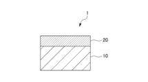
- FIG. 1 is a cross-sectional view showing an example of an electrical contact material according to an embodiment.
- FIG. 2 is a sectional view showing another example of the electrical contact material of the embodiment.
- the present inventors focused on the amount of strain in the silver-containing layer provided on at least a portion of the surface of the conductive base material, and by controlling the CI value of the silver-containing layer, The inventors have discovered that the wear resistance of contact materials is excellent regardless of the characteristics of the conductive base material, and have completed the present disclosure based on this knowledge.
- the electrical contact material of the embodiment includes an electrically conductive base material and a silver-containing layer containing silver provided on at least a portion of the surface of the electrically conductive base material, and in a cross section of the electrical contact material, the silver-containing layer
- the average CI value of is 0.6 or more.
- FIG. 1 is a cross-sectional view showing an example of an electrical contact material according to an embodiment.
- the electrical contact material 1 includes a conductive base material 10 and a silver-containing layer 20.
- the conductive base material 10 constituting the electrical contact material 1 is a rolled material that has conductivity and is obtained by rolling.
- the conductive base material 10 is made of a copper-based material containing pure copper and a copper alloy, or an iron-based material containing pure iron and an iron alloy.
- it is made of a material.
- Cu-Zn based, Cu-Ni-Si based, Cu-Sn-Ni based, Cu-Cr-Mg based, and Cu-Ni-Si-Zn-Sn-Mg based copper alloys are preferred. .
- the electrical conductivity of the conductive base material 10 is preferably 60% IACS or more, more preferably 80% IACS or more. When the electrical conductivity of the conductive base material 10 is 60% IACS or more, the electrical contact material 1 has good electrical conductivity.
- the shape of the conductive base material 10 may be appropriately selected depending on the use of the electrical contact material 1, but it is preferably strip-shaped, plate-shaped, rod-shaped, or linear.
- the silver-containing layer 20 constituting the electrical contact material 1 is provided on at least a portion of the surface of the conductive base material 10 and contains silver.
- the silver-containing layer 20 covering the surface of the conductive substrate 10 is made of pure silver or a silver alloy, preferably a silver alloy, that is, the silver-containing layer 20 is preferably a silver alloy layer. From the viewpoint that the electrical contact material 1 has excellent abrasion resistance and the abrasion resistance of the electrical contact material 1 is not easily influenced by the characteristics of the conductive base material 10, the silver-containing layer 20 is formed by plating, i.e. It is preferable that the silver-containing layer 20 is a plating film.
- the average CI value of the silver-containing layer 20 is 0.6 or more.
- the cross section of the electrical contact material 1 is a cross section parallel to the rolling direction of the conductive base material 10.
- the second element dissolves in solid solution in the silver crystals in the silver-containing layer 20, improving crystallinity and increasing the coefficient of dynamic friction. Since the hardness is low and high hardness can be maintained, wear resistance can be improved. The higher the average CI value, the higher the reliability of the crystal orientation. From this point of view, the average CI value of the silver-containing layer 20 in the cross section of the electrical contact material 1 is 0.6 or more, and the higher the CI value, the more preferable.
- the average IQ value of the silver-containing layer 20 is preferably 1000 or more, more preferably 1500 or more.
- the crystal quality is good.
- the average IQ value of the silver-containing layer 20 is preferably 2100 or less, more preferably 2000 or less.
- the average IQ value of the silver-containing layer 20 is 2100 or less, the crystal lattice is sufficiently distorted and the strain increases, so that wear resistance can be improved.
- the CI (Confidence Index) value is a value used to index patterns, an index for evaluating whether the calculated crystal orientation is correct, and a value used for evaluating whether the calculated crystal orientation is correct.
- the CI value is a value that reflects the reliability of the crystal orientation within the silver-containing layer 20.
- the IQ (Image Quality) value is a value obtained by plotting the peak intensity indicating a band in the Hough space when the EBSD pattern is Hough-transformed, and its size indicates the good crystallinity in the silver-containing layer 20. , is a value that reflects the amount of distortion.
- CI values and IQ values were measured continuously using an EBSD detector (manufactured by TSL Solutions, OIM5.0 HIKARI) attached to a high-resolution scanning analytical electron microscope (manufactured by JEOL Ltd., JSM-7001FA). It can be obtained from crystal orientation analysis data calculated from orientation data using analysis software (OIM Analysis, manufactured by TSL Solutions).
- the object to be measured is the surface of the silver-containing layer 20 on the cross section of the electrical contact material 1 parallel to the rolling direction of the conductive base material 10, which has been mirror-finished using a cross-section polisher (manufactured by JEOL Ltd.), and the measurement magnification is 30,000. It's double.
- Measurement is performed in steps with a measurement interval of 50 nm or less, excluding measurement points whose CI value analyzed by analysis software is 0.1 or less (noise removal), and where the orientation difference between adjacent pixels is 5.00° or more.
- the boundaries are regarded as grain boundaries, and the CI value and IQ value of the silver-containing layer 20 are obtained.
- the average CI value and average IQ value of the silver-containing layer 20 can be obtained by performing this measurement multiple times (in multiple different measurement regions of the same sample) and calculating the average value.
- the average CI value and the average IQ value are the average values of the CI value and the IQ value in the measurement area of the silver-containing layer measured at a magnification of 30,000 times.
- the silver-containing layer 20 preferably contains one or more elements (hereinafter also referred to as a second element) selected from the group consisting of Sn, Zn, In, Ni, Cu, Se, Sb, and Co.
- a second element selected from the group consisting of Sn, Zn, In, Ni, Cu, Se, Sb, and Co.
- the silver-containing layer 20 is made of one or more types selected from the group consisting of Sn, Zn, In, Ni, Cu, Se, Sb, and Co.
- the total content of the elements is less than 15.0 at%.
- the silver-containing layer 20 is selected from the group consisting of Sn, Zn, In, Ni, Cu, Se, Sb, and Co. It is preferable that the total content of one or more elements is 0.1 at% or more.
- the lower limit of the average thickness of the silver-containing layer 20 is preferably 0.5 ⁇ m or more, more preferably 2.0 ⁇ m or more, and still more preferably 3.0 ⁇ m or more.
- the upper limit of the average thickness of the silver-containing layer 20 is preferably 5.0 ⁇ m or less.
- the lower limit of the average thickness of the silver-containing layer 20 is 0.5 ⁇ m or more, the excellent wear resistance of the electrical contact material 1 can be maintained for a long period of time.
- the upper limit of the average thickness of the silver-containing layer 20 is 5.0 ⁇ m or less, material costs can be suppressed.
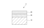
- FIG. 2 is a sectional view showing another example of the electrical contact material of the embodiment.
- the electrical contact material 2 shown in FIG. 2 has basically the same structure as the electrical contact material 1 shown in FIG. 1 except that the structure of the intermediate layer 30 is added.
- the electrical contact material 2 further includes an intermediate layer 30 made of nickel or a nickel alloy between the conductive base material 10 and the silver-containing layer 20.
- an intermediate layer 30 made of nickel or a nickel alloy between the conductive base material 10 and the silver-containing layer 20.
- the intermediate layer 30 is provided between the surface of the conductive base material 10 and the silver-containing layer 20, thermal diffusion of elements constituting the conductive base material 10 into the silver-containing layer 20 is suppressed, and the conductive base material The adhesion between the silver-containing layer 10 and the silver-containing layer 20 can be improved.
- the intermediate layer 30 is preferably made of pure nickel or a Ni-P-based nickel alloy.
- the lower limit of the average thickness of the intermediate layer 30 is preferably 0.01 ⁇ m or more, more preferably 0.10 ⁇ m or more, and still more preferably 0.30 ⁇ m or more.
- the upper limit of the average thickness of the intermediate layer 30 is preferably 3.00 ⁇ m or less, more preferably 2.00 ⁇ m or less, and still more preferably 1.00 ⁇ m or less. If the lower limit of the average thickness of the intermediate layer 30 is less than 0.01 ⁇ m, the above-mentioned suppression of thermal diffusion and improvement of adhesion cannot be achieved. If the upper limit of the average thickness of the intermediate layer 30 is more than 3.00 ⁇ m, bending workability deteriorates. When an electrical contact material is used in a terminal, bending workability of R/t ⁇ 1 is required.
- the electrical contact materials 1 and 2 described above may further include a copper layer (not shown) directly below the silver-containing layer 20, which is the surface layer.
- the copper layer (not shown) is made of pure copper or a copper alloy.
- the thickness of the copper layer (not shown) is significantly smaller than the thickness of the conductive base material 10.
- the electrical contact materials 1 and 2 have excellent abrasion resistance that is not easily affected by the characteristics of the conductive base material 10, so the electrical contact materials 1 and 2 are suitable for contacts, terminals, and connectors. Can be used. These contacts are contacts made using electrical contact materials 1 and 2, terminals are terminals made using electrical contact materials 1 and 2, and connectors are made using electrical contact materials 1 and 2. This is a connector made using
- a silver-containing layer is formed on at least a portion of the surface of a conductive base material by a plating method or the like. Subsequently, the base material provided with the silver-containing layer on the surface is rolled. In this way, the electrical contact material 1 can be manufactured.
- an intermediate layer is formed on at least a portion of the surface of the conductive base material by a plating method or the like.
- a silver-containing layer is formed on the intermediate layer by a plating method or the like.
- the substrate comprising the intermediate layer and the silver-containing layer is rolled. In this way, the electrical contact material 2 can be manufactured.
- the plating conditions for the silver-containing layer by setting the current density to 5 A/dm 2 or more and 10 A/dm 2 or less and the bath temperature (liquid temperature) to 25°C or more to prioritize nucleation, crystal grains with different crystal orientations can be formed. Since the silver-containing layer grows in large numbers and the difference in crystal orientation increases, the internal stress of the silver-containing layer can be further increased. By controlling the current density and temperature within the above range, the amount of strain in the silver-containing layer can be controlled. Even if the temperature is 25°C or higher, if the current density is less than 5 A/ dm2 , the crystal grains will become coarse, the number of crystal grains with different crystal orientations will decrease, and the amount of strain in the silver-containing layer will decrease.
- the lower limit is 20% or more, preferably 25% or more, and the upper limit is 30% or less.
- the processing rate is 20% or more, the amount of strain in the silver-containing layer can be increased and wear resistance can be improved.
- the processing rate is 30% or less, deterioration in bending workability due to excessive strain in the silver-containing layer can be suppressed.
- the processing rate of rolling is a percentage obtained by dividing the difference between the cross-sectional area of the sample before rolling and the cross-sectional area of the sample after rolling by the cross-sectional area of the sample before rolling.
- heat treatment is performed at 300° C. or higher and 600° C. or lower for 5 seconds or more and 60 seconds or less.
- the strain introduced by plating can be made uniform.
- the strain within the crystal grains is released, thereby making it possible to control the average CI value of the silver-containing layer to 0.6 or more.
- the strain within the crystal grains is released, thereby making it possible to control the average CI value of the silver-containing layer to 0.6 or more.
- crystallinity improves. As a result, control of the CI value and IQ value within a predetermined range is improved.
- the heat treatment temperature is less than 300°C or the heat treatment time is less than 5 seconds, the strain within the crystal grains cannot be sufficiently released and the strain cannot be concentrated near the grain boundaries, so the average CI value will be 0. It becomes less than .6.
- the heat treatment temperature exceeds 600°C and/or the heat treatment time exceeds 60 seconds, the average CI value will similarly exceed 0.6, and the material strength will decrease due to excessive heat treatment, causing contact , cannot maintain sufficient strength when used in terminals and connectors.
- a plating method using a plating bath containing the silver-containing component and the second element component is used.
- a silver-containing layer containing two elements may be directly formed.
- a silver-containing layer containing a second element may be formed by alternately forming a silver-containing layer and a second element layer by plating or the like, and then performing heat treatment. good.
- the processing rate of the rolling process is preferably 20% or more and 30% or less from the same viewpoint as above.
- the heat treatment in this case may be replaced by a heat treatment performed after forming the above-described silver-containing layer and before rolling.
- Examples 1-2, 17 The base material (manufactured by Furukawa Electric, EFTEC-550T, 80% IACS) was electrolytically degreased and then acid washed. Thereafter, a silver-containing layer was formed on the substrate surface by plating (current density 10 A/dm 2 ) in an alkali cyanide silver bath (silver cyanide 50 g/L, potassium cyanide 100 g/L) at a bath temperature of 25°C, and then Heat treatment was performed at 300° C. or higher and 600° C. or lower for 5 seconds or more and 60 seconds or less. Subsequently, electrical contact materials having the silver-containing layer (pure silver layer) shown in Table 1 were manufactured by rolling at the processing rate shown in Table 1.
- Examples 3, 10, 11, 18, 25, 26 The base material (manufactured by Furukawa Electric, EFTEC-550T, 80% IACS) was electrolytically degreased and then acid washed. Thereafter, a silver-containing layer was formed on the substrate surface by plating (current density 10 A/dm 2 ) in an alkali cyanide silver bath (silver cyanide 50 g/L, potassium cyanide 100 g/L) at a bath temperature of 25°C, and then A tin layer is formed by plating method (current density 10 A/dm 2 ) in a sulfuric acid bath (tin sulfate 80 g/L, sulfuric acid 80 g/L) at a bath temperature of 25°C, and then heated at 300°C or higher and 600°C or lower for 5 seconds or more. Heat treatment was performed for 60 seconds or less. Subsequently, electrical contact materials having the silver-containing layer (silver alloy layer) shown in Table 1 were manufactured by rolling at the processing rate
- Example 4 The base material (manufactured by Furukawa Electric, EFTEC-550T, 80% IACS) was electrolytically degreased and then acid washed. After that, alkali cyanide silver bath (silver cyanide 50-100 g/L, potassium cyanide 100-200 g/L, zinc chloride 10 g/L (Example 4), copper chloride dihydrate 12 g/L (example 4), bath temperature 25 ° C. Example 7), 10 g/L of nickel chloride (Example 29)) was used to form a silver-containing layer containing a second element on the surface of the substrate by plating (current density 5 to 10 A/dm 2 ), and then heated to 300°C. Heat treatment was performed at 600° C. or higher for 5 seconds or more and 60 seconds. Subsequently, electrical contact materials having the silver-containing layer (silver alloy layer) shown in Table 1 were manufactured by rolling at the processing rate shown in Table 1.
- Example 5 The base material (manufactured by Furukawa Electric, EFTEC-550T, 80% IACS) was electrolytically degreased and then acid washed. Thereafter, the intermediate layer was plated using a plating method (current density 10 A/dm 2 ) in a nickel plating bath (nickel sulfate hexahydrate 500 g/L, nickel chloride 30 g/L, boric acid 30 g/L) at a bath temperature of 55°C.
- a plating method current density 10 A/dm 2
- nickel plating bath nickel sulfate hexahydrate 500 g/L, nickel chloride 30 g/L, boric acid 30 g/L
- an alkali cyanide silver bath (silver cyanide 50-100 g/L, potassium cyanide 100-200 g/L, indium trichloride 15 g/L) at a bath temperature of 25°C to form a silver-containing layer containing a second element.
- a layer was formed on the surface of the intermediate layer by a plating method (current density 5 to 10 A/dm 2 ), followed by heat treatment at 300° C. to 600° C. for 5 seconds to 60 seconds. Subsequently, rolling was performed at the processing rates shown in Table 1 to produce electrical contact materials having the silver-containing layer (silver alloy layer) and intermediate layer (pure nickel layer) shown in Table 1.
- a nickel plating bath (nickel sulfate hexahydrate 500 g/L, nickel chloride 30 g/L, boric acid 30 g/L) at a bath temperature of 55°C (Comparative Examples 2, 5-6, 10, 13-14, 18, 21-22, 26, 29-30, 34, 38, 42, 46, 50, 54, 58, 62) or a nickel-phosphorous electrolytic bath with a bath temperature of 55°C (nickel sulfate hexahydrate 500g/L, chloride Nickel hexahydrate 30g/L, boric acid 30g/L, phosphorous acid 16g/L) (Comparative Examples 4, 7-8, 12, 15-16, 20, 23-24, 28, 31-32, 36 , 39-40, 43, 47-48, 52, 56, 60, 64), an intermediate layer was formed on the surface of the substrate by plating (current density 15 A/dm 2 ), and then an alkali layer was formed at a bath temperature of 25°C.
- Cyanide silver bath (silver cyanide 50-100g/L, potassium cyanide 100-200g/L, zinc chloride 10g/L (Comparative Examples 2, 10, 18, 26, 34, 43, 52, 60), nickel chloride 10g/L (Comparative Examples 4, 12, 20, 28, 36, 46, 54, 62), copper chloride dihydrate 12 g/L (Comparative Examples 5, 13, 21, 29, 38, 47), potassium selenocyanate 2.
- Example 14 The base material (manufactured by Furukawa Electric, EFTEC-550T, 80% IACS) was electrolytically degreased and then acid washed. Thereafter, a silver-containing layer containing a second element was formed by plating (current It was formed on the surface of the substrate at a density of 5 to 10 A/dm 2 ), and then heated at 300° C. to 600° C. for 5 seconds to 60 seconds. Subsequently, electrical contact materials having the silver-containing layer (silver alloy layer) shown in Table 1 were manufactured by rolling at the processing rate shown in Table 1.
- Example 19 The base material (manufactured by Furukawa Electric, EFTEC-550T, 80% IACS) was electrolytically degreased and then acid washed. Thereafter, a silver-containing layer containing a second element was formed by plating (current density 10A) in an alkali cyanide silver bath (silver cyanide 100g/L, potassium cyanide 200g/L, potassium selenocyanate 2.2mg/L) at a bath temperature of 25°C. /dm 2 ) on the surface of the substrate, followed by heat treatment at 300° C. to 600° C. for 5 seconds to 60 seconds. Subsequently, electrical contact materials having the silver-containing layer (silver alloy layer) shown in Table 1 were manufactured by rolling at the processing rate shown in Table 1.
- a silver-containing layer is then formed on the surface of the intermediate layer by plating (current density 10 A/dm 2 ) in an alkali cyanide silver bath (silver cyanide 50 g/L, potassium cyanide 100 g/L) at a bath temperature of 25°C. Then, a tin layer was formed by plating method (current density 10 A/dm 2 ) in a sulfuric acid bath (tin sulfate 80 g/L, sulfuric acid 80 g/L) at a bath temperature of 25°C, and then at a temperature lower than 300°C or Heat treatment was performed at a temperature higher than 600° C. for less than 5 seconds. Subsequently, rolling was carried out at the processing rates shown in Table 2 to produce electrical contact materials having the silver-containing layer (silver alloy layer) and intermediate layer (pure nickel layer) shown in Table 2.
- the surface of the silver-containing layer on the mirror-finished surface of the cross section of the electrical contact material parallel to the rolling direction of the conductive base material was obtained as the measurement target.
- the measurement magnification was 30,000 times. Measurement is performed in steps with a measurement interval of 50 nm or less, excluding measurement points with a CI value of 0.1 or less analyzed by analysis software, and boundaries where the orientation difference between adjacent pixels is 5.00° or more are defined as crystal grains.
- the CI value and IQ value of the silver-containing layer were obtained. This measurement was performed five times (in five different measurement areas of the same sample), and the average value was calculated to obtain the average CI value and average IQ value of the silver-containing layer.
- Dynamic friction coefficient is less than 0.3 ⁇ : Dynamic friction coefficient is 0.3 or more and less than 0.5 ⁇ : Dynamic friction coefficient is 0.5 or more
- Abrasion resistance The surface of the electrical contact material on the silver-containing layer side was tested using a friction and wear tester Tribogear (surface property measuring device TYPE: 14FW, manufactured by Shinto Kagaku Co., Ltd.) under a contact load of 4 N. Reciprocating sliding was performed 50 times at a moving distance of 50 mm and a sliding speed of 100 mm/min. Using a laser roughness meter, the ratio of the depth from the reference surface (the surface that was not sliding back and forth) to the thickness of the silver-containing layer was measured. The wear resistance was ranked as follows.
- ⁇ The ratio of the depth from the reference plane to the thickness of the silver-containing layer is less than 1/10.
- ⁇ The ratio of the depth from the reference plane to the thickness of the silver-containing layer is 1/10 or more and less than 1/5.
- ⁇ The ratio of the depth from the reference plane to the thickness of the silver-containing layer is 1/5 or more
- ⁇ Contact resistance value is less than 0.5 m ⁇ ⁇ : Contact resistance value is 0.5 m ⁇ or more and less than 1.0 m ⁇ ⁇ : Contact resistance value is 1.0 m ⁇ or more
- ⁇ Contact resistance value after heating is less than 1.0 m ⁇ ⁇ : Contact resistance value after heating is 1.0 m ⁇ or more and less than 5.0 m ⁇ ⁇ : Contact resistance value after heating is 5.0 m ⁇ or more
- the average CI value of the silver-containing layer was 0.6 or more, so the wear resistance of the electrical contact material was influenced by the characteristics of the conductive base material. I didn't receive it and it was good. On the other hand, in Comparative Examples 1 to 64, the average CI value of the silver-containing layer was outside the range of 0.6 or more, so the wear resistance of the electrical contact material was poor.
Landscapes
- Chemical & Material Sciences (AREA)
- Engineering & Computer Science (AREA)
- Materials Engineering (AREA)
- Metallurgy (AREA)
- Organic Chemistry (AREA)
- Chemical Kinetics & Catalysis (AREA)
- Electrochemistry (AREA)
- Mechanical Engineering (AREA)
- Contacts (AREA)
Abstract
This electrical contact material comprises: a conductive substrate; and a silver-containing layer which contains silver and is provided on at least a part of the surface of the conductive substrate, wherein the average CI value of the silver-containing layer in the cross-section of the electrical contact material is at least is 0.6.
Description
本開示は、電気接点材料、ならびにこれを用いた接点、端子およびコネクタに関する。
The present disclosure relates to electrical contact materials, and contacts, terminals, and connectors using the same.
近年、自動車では、省燃費化を達成するために、車両駆動方式の電動化が進行している。車両駆動方式の電動化に伴い、電池‐インバータ‐モータ間の電線の通電量が飛躍的に増加する一方で、接点やコネクタの通電時の発熱が問題となる。そのため、接点やコネクタには導電率の高い純銅や希薄銅合金、コルソン合金の表面に対してニッケルの下地めっきを施し、さらに下地めっきの上に銀または銀合金のめっきを施した材料が使用されている。しかしながら、銀は凝着摩耗しやすい金属種であることから、銀めっきは摺動時に削れやすい。そのため、銀めっきの摩耗によって、銀めっき材の接触抵抗が上昇してしまうという欠点があった。
In recent years, in order to achieve fuel efficiency in automobiles, the electrification of vehicle drive systems is progressing. With the electrification of vehicle drive systems, the amount of current flowing through the wires between the battery, inverter, and motor increases dramatically, but the heat generated when the contacts and connectors are energized becomes a problem. Therefore, materials used for contacts and connectors include highly conductive pure copper, diluted copper alloy, or Corson alloy, with a nickel base plating applied to the surface, and then silver or silver alloy plating applied on top of the base plating. ing. However, since silver is a metal that is prone to adhesive wear, the silver plating is likely to be scraped off during sliding. Therefore, there was a drawback that the contact resistance of the silver plating material increased due to wear of the silver plating.
このような欠点に対して、例えば特許文献1には、銅又は銅合金からなる母材の表面が銀めっき層により被覆され、銀めっき層が、下層側の第1銀めっき層と、第1銀めっき層の上層側の第2銀めっき層とからなり、第1銀めっき層の結晶粒径が第2銀めっき層の結晶粒径よりも大きい、コネクタ用銀めっき端子が記載されている。特許文献1では、銀めっき材について、再結晶により銀めっき層の結晶粒径が増大し易く、この結晶粒径の増大により硬度が低くなって、耐摩耗性が低下するという問題に対して、耐摩耗性の良い材料として銀めっき層の結晶粒径の大きさを規定している。しかしながら、結晶粒径の大きさは、めっき層の厚さに依存する。そのため、特許文献1で良好な耐摩耗性を得るためには、銀めっき層の厚さの制約がある。
To deal with such drawbacks, for example, Patent Document 1 discloses that the surface of a base material made of copper or copper alloy is coated with a silver plating layer, and the silver plating layer is separated from the first silver plating layer on the lower layer side and the first silver plating layer. A silver-plated terminal for a connector is described, which is composed of a second silver-plated layer above a silver-plated layer, and in which the crystal grain size of the first silver-plated layer is larger than the crystal grain size of the second silver-plated layer. Patent Document 1 discloses that, regarding silver-plated materials, the crystal grain size of the silver-plated layer tends to increase due to recrystallization, and this increase in crystal grain size lowers hardness and reduces wear resistance. The crystal grain size of the silver plating layer is specified as a material with good wear resistance. However, the size of the crystal grains depends on the thickness of the plating layer. Therefore, in order to obtain good wear resistance in Patent Document 1, there is a restriction on the thickness of the silver plating layer.
また、特許文献2には、所定濃度の銀とシアン化カリウムとセレンとを含む銀めっき液中において、銀めっき液中のシアン化カリウムの濃度と電流密度の積をy、液温をxとして、yおよびxを所定関係になるように電気めっきを行うことによって、素材である基材上に純度99.9質量%以上の銀めっき皮膜を形成する、銀めっき材の製造方法が記載されている。特許文献2は、銀めっき皮膜中にセレンなどの元素を含有させることにより、高い硬度を維持したまま接触抵抗の増加を抑制した銀めっき材の製造方法を例示しており、銀めっき材表面のビッカース硬さを耐摩耗性の根拠としている。このように、特許文献2では、基材の特性に依存する銀めっき材のビッカース硬さを耐摩耗性の評価に用いている。しかしながら、本来は、基材特性の影響を受けにくいめっき皮膜自体の耐摩耗性を評価する必要がある。
Furthermore, in Patent Document 2, in a silver plating solution containing silver, potassium cyanide, and selenium at a predetermined concentration, y and x are A method for producing a silver-plated material is described in which a silver plating film with a purity of 99.9% by mass or more is formed on a base material by electroplating so that a predetermined relationship is achieved. Patent Document 2 exemplifies a method for manufacturing a silver-plated material that suppresses an increase in contact resistance while maintaining high hardness by containing elements such as selenium in the silver-plated film, and Vickers hardness is the basis for wear resistance. In this manner, in Patent Document 2, the Vickers hardness of the silver-plated material, which depends on the characteristics of the base material, is used to evaluate the wear resistance. However, it is originally necessary to evaluate the wear resistance of the plating film itself, which is not easily affected by the characteristics of the base material.
本開示の目的は、基材特性の影響を受けにくい優れた耐摩耗性を有する電気接点材料、ならびにこれを用いた接点、端子およびコネクタを提供することである。
An object of the present disclosure is to provide an electrical contact material with excellent wear resistance that is not easily affected by base material properties, and contacts, terminals, and connectors using the same.
[1] 導電性基材と、前記導電性基材の表面の少なくとも一部に設けられる銀を含む銀含有層とを備える電気接点材料であって、前記電気接点材料の断面において、前記銀含有層の平均CI値は0.6以上である、電気接点材料。
[2] 前記電気接点材料の断面において、前記銀含有層の平均IQ値は1000以上2100以下である、上記[1]に記載の電気接点材料。
[3] 前記銀含有層は、Sn、Zn、In、Ni、Cu、Se、SbおよびCoからなる群より選択される1種以上の元素を含む、上記[1]または[2]に記載の電気接点材料。
[4] 前記銀含有層は、Sn、Zn、In、Ni、Cu、Se、SbおよびCoからなる群より選択される1種以上の元素を合計で15.0at%未満含む、上記[1]~[3]のいずれか1つに記載の電気接点材料。
[5] 前記銀含有層の平均厚さは0.5μm以上5.0μm以下である、上記[1]~[4]のいずれか1つに記載の電気接点材料。
[6] 前記導電性基材と前記銀含有層との間に、ニッケルまたはニッケル合金からなる中間層をさらに備える、上記[1]~[5]のいずれか1つに記載の電気接点材料。
[7] 前記中間層の平均厚さは0.01μm以上3.00μm以下である、上記[6]に記載の電気接点材料。
[8] 上記[1]~[7]のいずれか1つに記載の電気接点材料を用いて作製された接点。
[9] 上記[1]~[7]のいずれか1つに記載の電気接点材料を用いて作製された端子。
[10] 上記[1]~[7]のいずれか1つに記載の電気接点材料を用いて作製されたコネクタ。 [1] An electrical contact material comprising an electrically conductive base material and a silver-containing layer containing silver provided on at least a part of the surface of the electrically conductive base material, wherein the silver-containing layer is provided in a cross section of the electrical contact material. An electrical contact material, wherein the layer has an average CI value of 0.6 or more.
[2] The electrical contact material according to [1] above, wherein in the cross section of the electrical contact material, the average IQ value of the silver-containing layer is 1000 or more and 2100 or less.
[3] The silver-containing layer according to [1] or [2] above contains one or more elements selected from the group consisting of Sn, Zn, In, Ni, Cu, Se, Sb and Co. Electrical contact materials.
[4] The above-mentioned [1], wherein the silver-containing layer contains a total of less than 15.0 at% of one or more elements selected from the group consisting of Sn, Zn, In, Ni, Cu, Se, Sb, and Co. The electrical contact material according to any one of ~[3].
[5] The electrical contact material according to any one of [1] to [4] above, wherein the average thickness of the silver-containing layer is 0.5 μm or more and 5.0 μm or less.
[6] The electrical contact material according to any one of [1] to [5] above, further comprising an intermediate layer made of nickel or a nickel alloy between the conductive base material and the silver-containing layer.
[7] The electrical contact material according to [6] above, wherein the intermediate layer has an average thickness of 0.01 μm or more and 3.00 μm or less.
[8] A contact produced using the electrical contact material according to any one of [1] to [7] above.
[9] A terminal produced using the electrical contact material according to any one of [1] to [7] above.
[10] A connector manufactured using the electrical contact material according to any one of [1] to [7] above.
本開示によれば、基材特性の影響を受けにくい優れた耐摩耗性を有する電気接点材料、ならびにこれを用いた接点、端子およびコネクタを提供することができる。
According to the present disclosure, it is possible to provide an electrical contact material having excellent wear resistance that is not easily affected by base material properties, and contacts, terminals, and connectors using the same.
以下、実施形態に基づき詳細に説明する。
Hereinafter, it will be described in detail based on the embodiment.
本発明者らは、鋭意研究を重ねた結果、導電性基材の表面の少なくとも一部に設けられる銀含有層中の歪量に着目し、銀含有層のCI値を制御することによって、電気接点材料の耐摩耗性が導電性基材の特性に依存せずに優れていることを見出し、かかる知見に基づき本開示を完成させるに至った。
As a result of extensive research, the present inventors focused on the amount of strain in the silver-containing layer provided on at least a portion of the surface of the conductive base material, and by controlling the CI value of the silver-containing layer, The inventors have discovered that the wear resistance of contact materials is excellent regardless of the characteristics of the conductive base material, and have completed the present disclosure based on this knowledge.
実施形態の電気接点材料は、導電性基材と、前記導電性基材の表面の少なくとも一部に設けられる銀を含む銀含有層とを備え、前記電気接点材料の断面において、前記銀含有層の平均CI値は0.6以上である。
The electrical contact material of the embodiment includes an electrically conductive base material and a silver-containing layer containing silver provided on at least a portion of the surface of the electrically conductive base material, and in a cross section of the electrical contact material, the silver-containing layer The average CI value of is 0.6 or more.
図1は、実施形態の電気接点材料の一例を示す断面図である。図1に示すように、電気接点材料1は、導電性基材10と銀含有層20とを備える。
FIG. 1 is a cross-sectional view showing an example of an electrical contact material according to an embodiment. As shown in FIG. 1, the electrical contact material 1 includes a conductive base material 10 and a silver-containing layer 20.
電気接点材料1を構成する導電性基材10は、導電性を有し、圧延加工で得られる圧延材である。導電性基材10の圧延加工性および電気接点材料1の高導電性などの観点から、導電性基材10は、純銅および銅合金を含む銅系材料、または純鉄および鉄合金を含む鉄系材料から構成されることが好ましい。そのなかでも、Cu-Zn系、Cu-Ni-Si系、Cu-Sn-Ni系、Cu-Cr-Mg系、Cu-Ni-Si-Zn-Sn-Mg系の銅合金であることが好ましい。
The conductive base material 10 constituting the electrical contact material 1 is a rolled material that has conductivity and is obtained by rolling. From the viewpoints of rolling workability of the conductive base material 10 and high conductivity of the electrical contact material 1, the conductive base material 10 is made of a copper-based material containing pure copper and a copper alloy, or an iron-based material containing pure iron and an iron alloy. Preferably, it is made of a material. Among these, Cu-Zn based, Cu-Ni-Si based, Cu-Sn-Ni based, Cu-Cr-Mg based, and Cu-Ni-Si-Zn-Sn-Mg based copper alloys are preferred. .
導電性基材10の電気伝導率は、好ましくは60%IACS以上、より好ましくは80%IACS以上である。導電性基材10の電気伝導率が60%IACS以上であると、電気接点材料1は良好な導電性を有する。
The electrical conductivity of the conductive base material 10 is preferably 60% IACS or more, more preferably 80% IACS or more. When the electrical conductivity of the conductive base material 10 is 60% IACS or more, the electrical contact material 1 has good electrical conductivity.
導電性基材10の形状は、電気接点材料1の用途に応じて適宜選択してもよいが、条状、板状、棒状または線状であることが好ましい。
The shape of the conductive base material 10 may be appropriately selected depending on the use of the electrical contact material 1, but it is preferably strip-shaped, plate-shaped, rod-shaped, or linear.
電気接点材料1を構成する銀含有層20は、導電性基材10の表面の少なくとも一部に設けられ、銀を含有する。導電性基材10の表面を覆う銀含有層20は、純銀または銀合金からなり、好ましくは銀合金からなる、すなわち、銀含有層20は銀合金層であることが好ましい。電気接点材料1が優れた耐摩耗性を有し、電気接点材料1の耐摩耗性が導電性基材10の特性の影響を受けにくい観点から、銀含有層20はめっきで形成される、すなわち銀含有層20はめっき皮膜であることが好ましい。
The silver-containing layer 20 constituting the electrical contact material 1 is provided on at least a portion of the surface of the conductive base material 10 and contains silver. The silver-containing layer 20 covering the surface of the conductive substrate 10 is made of pure silver or a silver alloy, preferably a silver alloy, that is, the silver-containing layer 20 is preferably a silver alloy layer. From the viewpoint that the electrical contact material 1 has excellent abrasion resistance and the abrasion resistance of the electrical contact material 1 is not easily influenced by the characteristics of the conductive base material 10, the silver-containing layer 20 is formed by plating, i.e. It is preferable that the silver-containing layer 20 is a plating film.
図1に示す電気接点材料1の断面において、銀含有層20の平均CI値は0.6以上である。電気接点材料1の断面とは、導電性基材10の圧延方向に平行な断面である。
In the cross section of the electrical contact material 1 shown in FIG. 1, the average CI value of the silver-containing layer 20 is 0.6 or more. The cross section of the electrical contact material 1 is a cross section parallel to the rolling direction of the conductive base material 10.
電気接点材料1の断面における銀含有層20の平均CI値が0.6以上であると、銀含有層20において銀の結晶中に第2元素が固溶して結晶性が向上し、動摩擦係数が低く、高硬度を維持できるため、耐摩耗性を向上できる。平均CI値が高いほど、結晶方位の信頼性が高い。このような観点から、電気接点材料1の断面における銀含有層20の平均CI値は、0.6以上であり、高いほど好ましい。
When the average CI value of the silver-containing layer 20 in the cross section of the electrical contact material 1 is 0.6 or more, the second element dissolves in solid solution in the silver crystals in the silver-containing layer 20, improving crystallinity and increasing the coefficient of dynamic friction. Since the hardness is low and high hardness can be maintained, wear resistance can be improved. The higher the average CI value, the higher the reliability of the crystal orientation. From this point of view, the average CI value of the silver-containing layer 20 in the cross section of the electrical contact material 1 is 0.6 or more, and the higher the CI value, the more preferable.
また、電気接点材料1の断面において、銀含有層20の平均IQ値は、1000以上であることが好ましく、1500以上であることがより好ましい。銀含有層20の平均IQ値が1000以上であると、結晶品質が良好である。
Furthermore, in the cross section of the electrical contact material 1, the average IQ value of the silver-containing layer 20 is preferably 1000 or more, more preferably 1500 or more. When the average IQ value of the silver-containing layer 20 is 1000 or more, the crystal quality is good.
また、電気接点材料1の断面において、銀含有層20の平均IQ値は、2100以下であることが好ましく、2000以下であることがより好ましい。銀含有層20の平均IQ値が2100以下であると、結晶格子が十分に歪み、歪が多くなることで、耐摩耗性を向上できる。
Furthermore, in the cross section of the electrical contact material 1, the average IQ value of the silver-containing layer 20 is preferably 2100 or less, more preferably 2000 or less. When the average IQ value of the silver-containing layer 20 is 2100 or less, the crystal lattice is sufficiently distorted and the strain increases, so that wear resistance can be improved.
CI(Confidence Index)値は、パターンの指数付け、算出した結晶方位が正しいのか評価するための指標、算出した結晶方位が正しいのか評価するのに用いる値である。CI値は、銀含有層20内の結晶方位の信頼性を反映した値である。
The CI (Confidence Index) value is a value used to index patterns, an index for evaluating whether the calculated crystal orientation is correct, and a value used for evaluating whether the calculated crystal orientation is correct. The CI value is a value that reflects the reliability of the crystal orientation within the silver-containing layer 20.
また、IQ(Image Quality)値は、EBSDパターンをHough変換した際のHough空間上のバンドを示すピーク強度をプロットした値であり、その大きさにより、銀含有層20内の結晶性の良好さ、歪量を反映した値である。
In addition, the IQ (Image Quality) value is a value obtained by plotting the peak intensity indicating a band in the Hough space when the EBSD pattern is Hough-transformed, and its size indicates the good crystallinity in the silver-containing layer 20. , is a value that reflects the amount of distortion.
CI値およびIQ値は、高分解能走査型分析電子顕微鏡(日本電子株式会社製、JSM-7001FA)に付属するEBSD検出器(TSLソリューションズ製、OIM5.0 HIKARI)を用いて連続して測定した結晶方位データから解析ソフト(TSLソリューションズ製、OIM Analysis)を用いて算出した結晶方位解析データから得ることができる。測定対象は、導電性基材10の圧延方向に平行な電気接点材料1の断面をクロスセクションポリッシャー(日本電子製)で鏡面仕上げされた表面における銀含有層20の表面であり、測定倍率は30000倍である。測定間隔50nm以下のステップで測定し、解析ソフトにより解析されたCI値が0.1以下である測定点を除外し(ノイズ除去)、隣接するピクセル間の方位差が5.00°以上である境界を結晶粒界とみなし、銀含有層20のCI値およびIQ値を得る。この測定を複数回(同一サンプルで異なる複数の測定領域)行い、その平均値を算出して、銀含有層20の平均CI値および平均IQ値を得ることができる。このように、平均CI値および平均IQ値は、倍率30000倍で測定した銀含有層の測定領域におけるCI値およびIQ値の平均値である。
CI values and IQ values were measured continuously using an EBSD detector (manufactured by TSL Solutions, OIM5.0 HIKARI) attached to a high-resolution scanning analytical electron microscope (manufactured by JEOL Ltd., JSM-7001FA). It can be obtained from crystal orientation analysis data calculated from orientation data using analysis software (OIM Analysis, manufactured by TSL Solutions). The object to be measured is the surface of the silver-containing layer 20 on the cross section of the electrical contact material 1 parallel to the rolling direction of the conductive base material 10, which has been mirror-finished using a cross-section polisher (manufactured by JEOL Ltd.), and the measurement magnification is 30,000. It's double. Measurement is performed in steps with a measurement interval of 50 nm or less, excluding measurement points whose CI value analyzed by analysis software is 0.1 or less (noise removal), and where the orientation difference between adjacent pixels is 5.00° or more. The boundaries are regarded as grain boundaries, and the CI value and IQ value of the silver-containing layer 20 are obtained. The average CI value and average IQ value of the silver-containing layer 20 can be obtained by performing this measurement multiple times (in multiple different measurement regions of the same sample) and calculating the average value. Thus, the average CI value and the average IQ value are the average values of the CI value and the IQ value in the measurement area of the silver-containing layer measured at a magnification of 30,000 times.
また、銀含有層20は、Sn、Zn、In、Ni、Cu、Se、SbおよびCoからなる群より選択される1種以上の元素(以下、第2元素ともいう)を含むことが好ましい。銀含有層20中に第2元素を共存させることで、摺動性を向上できる。そのなかでも、電気接点材料1の電気接続性を向上する観点から、銀含有層20は、Sn、Zn、In、Ni、Cu、Se、SbおよびCoからなる群より選択される1種以上の元素を合計で15.0at%未満含むことが好ましい。また、第2元素の添加による効率的な摺動性の向上および材料コスト抑制の観点から、銀含有層20は、Sn、Zn、In、Ni、Cu、Se、SbおよびCoからなる群より選択される1種以上の元素を合計で0.1at%以上含むことが好ましい。
Further, the silver-containing layer 20 preferably contains one or more elements (hereinafter also referred to as a second element) selected from the group consisting of Sn, Zn, In, Ni, Cu, Se, Sb, and Co. By making the second element coexist in the silver-containing layer 20, slidability can be improved. Among them, from the viewpoint of improving the electrical connectivity of the electrical contact material 1, the silver-containing layer 20 is made of one or more types selected from the group consisting of Sn, Zn, In, Ni, Cu, Se, Sb, and Co. Preferably, the total content of the elements is less than 15.0 at%. In addition, from the viewpoint of efficiently improving sliding properties and suppressing material costs by adding a second element, the silver-containing layer 20 is selected from the group consisting of Sn, Zn, In, Ni, Cu, Se, Sb, and Co. It is preferable that the total content of one or more elements is 0.1 at% or more.
銀含有層20の平均厚さの下限値は、好ましくは0.5μm以上、より好ましくは2.0μm以上、さらに好ましくは3.0μm以上である。銀含有層20の平均厚さの上限値は、好ましくは5.0μm以下である。銀含有層20の平均厚さの下限値が0.5μm以上であると、優れた電気接点材料1の耐摩耗性を長期間に亘って維持できる。銀含有層20の平均厚さの上限値が5.0μm以下であると、材料コストを抑制できる。
The lower limit of the average thickness of the silver-containing layer 20 is preferably 0.5 μm or more, more preferably 2.0 μm or more, and still more preferably 3.0 μm or more. The upper limit of the average thickness of the silver-containing layer 20 is preferably 5.0 μm or less. When the lower limit of the average thickness of the silver-containing layer 20 is 0.5 μm or more, the excellent wear resistance of the electrical contact material 1 can be maintained for a long period of time. When the upper limit of the average thickness of the silver-containing layer 20 is 5.0 μm or less, material costs can be suppressed.
図2は、実施形態の電気接点材料の他の例を示す断面図である。図2に示す電気接点材料2において、中間層30の構成が追加されること以外は、図1に示す電気接点材料1の構成と基本的に同じである。
FIG. 2 is a sectional view showing another example of the electrical contact material of the embodiment. The electrical contact material 2 shown in FIG. 2 has basically the same structure as the electrical contact material 1 shown in FIG. 1 except that the structure of the intermediate layer 30 is added.
図2に示すように、電気接点材料2は、導電性基材10と銀含有層20との間に、ニッケルまたはニッケル合金からなる中間層30をさらに備える。導電性基材10の表面と銀含有層20との間に中間層30が設けられると、導電性基材10を構成する元素の銀含有層20への熱拡散の抑制、および導電性基材10と銀含有層20との密着性を向上できる。
As shown in FIG. 2, the electrical contact material 2 further includes an intermediate layer 30 made of nickel or a nickel alloy between the conductive base material 10 and the silver-containing layer 20. When the intermediate layer 30 is provided between the surface of the conductive base material 10 and the silver-containing layer 20, thermal diffusion of elements constituting the conductive base material 10 into the silver-containing layer 20 is suppressed, and the conductive base material The adhesion between the silver-containing layer 10 and the silver-containing layer 20 can be improved.
上記の熱拡散の抑制および密着性をさらに向上する観点から、中間層30は、純ニッケル、またはNi-P系のニッケル合金であることが好ましい。
From the viewpoint of further improving the above-mentioned thermal diffusion suppression and adhesion, the intermediate layer 30 is preferably made of pure nickel or a Ni-P-based nickel alloy.
中間層30の平均厚さの下限値は、好ましくは0.01μm以上、より好ましくは0.10μm以上、さらに好ましくは0.30μm以上である。中間層30の平均厚さの上限値は、好ましくは3.00μm以下、より好ましくは2.00μm以下、さらに好ましくは1.00μm以下である。中間層30の平均厚さの下限値が0.01μm未満であると、上記の熱拡散の抑制および密着性の向上を達成できない。中間層30の平均厚さの上限値が3.00μm超であると、曲げ加工性が悪化する。電気接点材料を端子で使用する場合、R/t≧1の曲げ加工性が要求される。
The lower limit of the average thickness of the intermediate layer 30 is preferably 0.01 μm or more, more preferably 0.10 μm or more, and still more preferably 0.30 μm or more. The upper limit of the average thickness of the intermediate layer 30 is preferably 3.00 μm or less, more preferably 2.00 μm or less, and still more preferably 1.00 μm or less. If the lower limit of the average thickness of the intermediate layer 30 is less than 0.01 μm, the above-mentioned suppression of thermal diffusion and improvement of adhesion cannot be achieved. If the upper limit of the average thickness of the intermediate layer 30 is more than 3.00 μm, bending workability deteriorates. When an electrical contact material is used in a terminal, bending workability of R/t≧1 is required.
また、上記の電気接点材料1、2は、表層である銀含有層20の直下に、不図示の銅層をさらに備えてもよい。不図示の銅層は、純銅または銅合金から構成される。導電性基材10の厚さに比べて、不図示の銅層の厚さは大幅に小さい。電気接点材料1、2が銀含有層20の直下に不図示の銅層をさらに備えると、密着性および曲げ加工性を向上できる。
Furthermore, the electrical contact materials 1 and 2 described above may further include a copper layer (not shown) directly below the silver-containing layer 20, which is the surface layer. The copper layer (not shown) is made of pure copper or a copper alloy. The thickness of the copper layer (not shown) is significantly smaller than the thickness of the conductive base material 10. When the electrical contact materials 1 and 2 further include a copper layer (not shown) directly below the silver-containing layer 20, adhesion and bendability can be improved.
上記のように、電気接点材料1、2は、導電性基材10の特性の影響を受けにくい優れた耐摩耗性を有するため、電気接点材料1、2は、接点、端子、コネクタに好適に用いることができる。こうした接点は、電気接点材料1、2を用いて作製された接点であり、端子は、電気接点材料1、2を用いて作製された端子であり、コネクタは、電気接点材料1、2を用いて作製されたコネクタである。
As described above, the electrical contact materials 1 and 2 have excellent abrasion resistance that is not easily affected by the characteristics of the conductive base material 10, so the electrical contact materials 1 and 2 are suitable for contacts, terminals, and connectors. Can be used. These contacts are contacts made using electrical contact materials 1 and 2, terminals are terminals made using electrical contact materials 1 and 2, and connectors are made using electrical contact materials 1 and 2. This is a connector made using
次に、電気接点材料1、2の製造方法について説明する。
Next, a method for manufacturing the electrical contact materials 1 and 2 will be explained.
まず、導電性を有する基材の表面の少なくとも一部に、めっき法などによって銀含有層を形成する。続いて、銀含有層を表面に備える基材を圧延加工する。こうして、電気接点材料1を製造できる。
First, a silver-containing layer is formed on at least a portion of the surface of a conductive base material by a plating method or the like. Subsequently, the base material provided with the silver-containing layer on the surface is rolled. In this way, the electrical contact material 1 can be manufactured.
また、導電性を有する基材の表面の少なくとも一部に、めっき法などによって中間層を形成する。続いて、中間層の上に、めっき法などによって銀含有層を形成する。続いて、中間層および銀含有層を備える基材を圧延加工する。こうして、電気接点材料2を製造できる。
Further, an intermediate layer is formed on at least a portion of the surface of the conductive base material by a plating method or the like. Subsequently, a silver-containing layer is formed on the intermediate layer by a plating method or the like. Subsequently, the substrate comprising the intermediate layer and the silver-containing layer is rolled. In this way, the electrical contact material 2 can be manufactured.
銀含有層のめっき条件について、電流密度を5A/dm2以上10A/dm2以下、浴温(液温)を25℃以上にして、核生成を優先することで、異なる結晶方位の結晶粒が数多く成長し、結晶方位の差が大きくなることから、銀含有層の内部応力をさらに高めることができる。上記の範囲で電流密度及び温度を制御することにより、銀含有層内における歪量を制御できる。温度が25℃以上であっても、電流密度が5A/dm2未満であると、結晶粒は粗大となり、異なる結晶方位の結晶粒が少なくなり、銀含有層内の歪量が小さくなることで、接点、端子、コネクタで必要な耐摩耗性を満たすことができない。また、温度が25℃以上であっても、電流密度が10A/dm2超であると、微細化した結晶が過剰になることで、異なる結晶方位の結晶粒が多くなり、表面硬度が高すぎることで、曲げ加工性が劣る。
Regarding the plating conditions for the silver-containing layer, by setting the current density to 5 A/dm 2 or more and 10 A/dm 2 or less and the bath temperature (liquid temperature) to 25°C or more to prioritize nucleation, crystal grains with different crystal orientations can be formed. Since the silver-containing layer grows in large numbers and the difference in crystal orientation increases, the internal stress of the silver-containing layer can be further increased. By controlling the current density and temperature within the above range, the amount of strain in the silver-containing layer can be controlled. Even if the temperature is 25°C or higher, if the current density is less than 5 A/ dm2 , the crystal grains will become coarse, the number of crystal grains with different crystal orientations will decrease, and the amount of strain in the silver-containing layer will decrease. , contacts, terminals, and connectors cannot meet the required wear resistance. In addition, even if the temperature is 25°C or higher, if the current density exceeds 10 A/ dm2 , the refined crystals will become excessive, resulting in a large number of crystal grains with different crystal orientations, and the surface hardness will be too high. This results in poor bending workability.
また、圧延加工の加工率について、下限値は、20%以上であり、25%以上であることが好ましく、上限値は、30%以下である。加工率が20%以上であると、銀含有層中の歪量を増加して、耐摩耗性を向上できる。加工率が30%以下であると、銀含有層中の歪量が過剰になることによる、曲げ加工性の低下を抑制できる。圧延加工の加工率は、圧延加工前の試料の断面積と圧延加工後の試料の断面積との差を圧延加工前の試料の断面積で割った百分率である。
Regarding the processing rate of rolling, the lower limit is 20% or more, preferably 25% or more, and the upper limit is 30% or less. When the processing rate is 20% or more, the amount of strain in the silver-containing layer can be increased and wear resistance can be improved. When the processing rate is 30% or less, deterioration in bending workability due to excessive strain in the silver-containing layer can be suppressed. The processing rate of rolling is a percentage obtained by dividing the difference between the cross-sectional area of the sample before rolling and the cross-sectional area of the sample after rolling by the cross-sectional area of the sample before rolling.
また、銀含有層を形成した後であって圧延加工を行う前に、300℃以上600℃以下、5秒以上60秒以内の熱処理を実施する。この熱処理によって、めっきによって導入された歪を均一化できる。上記の範囲で熱処理を行うことにより、結晶粒内の歪を開放することで、銀含有層の平均CI値を0.6以上に制御できる。また、熱処理により結晶粒内の歪を開放することで、銀含有層内の歪は結晶粒界に多くの歪を集約できる。また、熱処理による合金化が進行することで、結晶性の良好さが向上する。その結果、CI値及びIQ値の所定範囲内への制御が向上する。熱処理について、熱処理温度が300℃未満および熱処理時間が5秒未満の少なくとも一方であると、結晶粒内の歪を十分に解放できず、歪を粒界近傍に集約できないため、平均CI値が0.6未満になる。熱処理について、熱処理温度が600℃超および熱処理時間が60秒超の少なくとも一方であっても、同様に平均CI値が0.6超になり、さらには熱処理が過剰で材料強度が低下し、接点、端子、コネクタに使用したときに十分な強度を保つことができない。
Further, after forming the silver-containing layer and before rolling, heat treatment is performed at 300° C. or higher and 600° C. or lower for 5 seconds or more and 60 seconds or less. By this heat treatment, the strain introduced by plating can be made uniform. By performing the heat treatment within the above range, the strain within the crystal grains is released, thereby making it possible to control the average CI value of the silver-containing layer to 0.6 or more. Furthermore, by releasing strain within the crystal grains through heat treatment, much of the strain within the silver-containing layer can be concentrated at the grain boundaries. Furthermore, as alloying progresses through heat treatment, crystallinity improves. As a result, control of the CI value and IQ value within a predetermined range is improved. Regarding heat treatment, if the heat treatment temperature is less than 300°C or the heat treatment time is less than 5 seconds, the strain within the crystal grains cannot be sufficiently released and the strain cannot be concentrated near the grain boundaries, so the average CI value will be 0. It becomes less than .6. Regarding heat treatment, even if the heat treatment temperature exceeds 600°C and/or the heat treatment time exceeds 60 seconds, the average CI value will similarly exceed 0.6, and the material strength will decrease due to excessive heat treatment, causing contact , cannot maintain sufficient strength when used in terminals and connectors.
また、第2元素を含む銀含有層20を備える電気接点材料1、2を製造する場合、上記のように、銀含有成分および第2元素成分を含むめっき浴を用いためっき法などによって、第2元素を含む銀含有層を直接形成してもよい。また、別の形成方法として、めっき法などによって、銀含有層と第2元素層とを交互に成膜した後、加熱処理を行うことで、第2元素を含む銀含有層を形成してもよい。この場合の圧延加工の加工率は、上記と同様の観点から、20%以上30%以下であることが好ましい。また、この場合の加熱処理は、上記した銀含有層を形成した後であって圧延加工を行う前に実施する熱処理によって代用されてもよい。
In addition, when manufacturing the electrical contact materials 1 and 2 provided with the silver-containing layer 20 containing the second element, as described above, a plating method using a plating bath containing the silver-containing component and the second element component is used. A silver-containing layer containing two elements may be directly formed. Alternatively, a silver-containing layer containing a second element may be formed by alternately forming a silver-containing layer and a second element layer by plating or the like, and then performing heat treatment. good. In this case, the processing rate of the rolling process is preferably 20% or more and 30% or less from the same viewpoint as above. Further, the heat treatment in this case may be replaced by a heat treatment performed after forming the above-described silver-containing layer and before rolling.
以上説明した実施形態によれば、導電性基材の表面に設けられる銀含有層中の歪量に着目し、銀含有層のCI値を制御することによって、基材特性の影響を受けにくい優れた耐摩耗性を有する電気接点材料を得ることができる。
According to the embodiment described above, by focusing on the amount of strain in the silver-containing layer provided on the surface of the conductive base material and controlling the CI value of the silver-containing layer, it is possible to achieve an advantage that is less affected by the base material properties. It is possible to obtain an electrical contact material having high wear resistance.
以上、実施形態について説明したが、本発明は上記実施形態に限定されるものではなく、本開示の概念および特許請求の範囲に含まれるあらゆる態様を含み、本開示の範囲内で種々に改変することができる。
Although the embodiments have been described above, the present invention is not limited to the above embodiments, but includes all aspects included in the concept of the present disclosure and the scope of the claims, and may be variously modified within the scope of the present disclosure. be able to.
次に、実施例および比較例について説明するが、本開示はこれら実施例に限定されるものではない。
Next, Examples and Comparative Examples will be described, but the present disclosure is not limited to these Examples.
(実施例1~2、17)
基材(古河電工製、EFTEC-550T、80%IACS)について、電解脱脂を行った後、酸洗浄を行った。その後、浴温25℃のアルカリシアン銀浴(シアン化銀50g/L、シアン化カリウム100g/L)にて銀含有層をめっき法(電流密度10A/dm2)で基材表面に形成し、続いて300℃以上600℃以下、5秒以上60秒以内の加熱処理を行った。続いて表1に示す加工率の圧延加工を行うことによって、表1に示す銀含有層(純銀層)を備える電気接点材料を製造した。 (Examples 1-2, 17)
The base material (manufactured by Furukawa Electric, EFTEC-550T, 80% IACS) was electrolytically degreased and then acid washed. Thereafter, a silver-containing layer was formed on the substrate surface by plating (current density 10 A/dm 2 ) in an alkali cyanide silver bath (silver cyanide 50 g/L, potassium cyanide 100 g/L) at a bath temperature of 25°C, and then Heat treatment was performed at 300° C. or higher and 600° C. or lower for 5 seconds or more and 60 seconds or less. Subsequently, electrical contact materials having the silver-containing layer (pure silver layer) shown in Table 1 were manufactured by rolling at the processing rate shown in Table 1.
(実施例3、10、11、18、25、26)
基材(古河電工製、EFTEC-550T、80%IACS)について、電解脱脂を行った後、酸洗浄を行った。その後、浴温25℃のアルカリシアン銀浴(シアン化銀50g/L、シアン化カリウム100g/L)にて銀含有層をめっき法(電流密度10A/dm2)で基材表面に形成し、続いて浴温25℃の硫酸浴(硫酸錫80g/L、硫酸80g/L)にて錫層をめっき法(電流密度10A/dm2)で形成し、続いて300℃以上600℃以下、5秒以上60秒以内の加熱処理を行った。続いて表1に示す加工率の圧延加工を行うことによって、表1に示す銀含有層(銀合金層)を備える電気接点材料を製造した。 (Examples 3, 10, 11, 18, 25, 26)
The base material (manufactured by Furukawa Electric, EFTEC-550T, 80% IACS) was electrolytically degreased and then acid washed. Thereafter, a silver-containing layer was formed on the substrate surface by plating (current density 10 A/dm 2 ) in an alkali cyanide silver bath (silver cyanide 50 g/L, potassium cyanide 100 g/L) at a bath temperature of 25°C, and then A tin layer is formed by plating method (current density 10 A/dm 2 ) in a sulfuric acid bath (tin sulfate 80 g/L, sulfuric acid 80 g/L) at a bath temperature of 25°C, and then heated at 300°C or higher and 600°C or lower for 5 seconds or more. Heat treatment was performed for 60 seconds or less. Subsequently, electrical contact materials having the silver-containing layer (silver alloy layer) shown in Table 1 were manufactured by rolling at the processing rate shown in Table 1.
(比較例49、57)
基材(古河電工製、EFTEC-550T、80%IACS)について、電解脱脂を行った後、酸洗浄を行った。その後、浴温25℃のアルカリシアン銀浴(シアン化銀50g/L、シアン化カリウム100g/L)にて銀含有層をめっき法(電流密度10A/dm2)で基材表面に形成し、続いて浴温25℃の硫酸浴(硫酸錫80g/L、硫酸80g/L)にて錫層をめっき法(電流密度10A/dm2)で形成し、300℃未満または600℃より高い温度で、5秒未満の加熱処理を行った。続いて表2に示す加工率の圧延加工を行うことによって、表2に示す銀含有層(銀合金層)を備える電気接点材料を製造した。 (Comparative Examples 49, 57)
The base material (manufactured by Furukawa Electric, EFTEC-550T, 80% IACS) was electrolytically degreased and then acid washed. Thereafter, a silver-containing layer was formed on the substrate surface by plating (current density 10 A/dm 2 ) in an alkali cyanide silver bath (silver cyanide 50 g/L, potassium cyanide 100 g/L) at a bath temperature of 25°C, and then A tin layer is formed by a plating method (current density 10 A/dm 2 ) in a sulfuric acid bath (80 g/L of tin sulfate, 80 g/L of sulfuric acid) at a bath temperature of 25°C, and at a temperature of less than 300°C or higher than 600°C. Heat treatment was performed for less than a second. Subsequently, electrical contact materials having the silver-containing layer (silver alloy layer) shown in Table 2 were manufactured by rolling at the processing rate shown in Table 2.
(実施例4、7、29)
基材(古河電工製、EFTEC-550T、80%IACS)について、電解脱脂を行った後、酸洗浄を行った。その後、浴温25℃のアルカリシアン銀浴(シアン化銀50~100g/L、シアン化カリウム100~200g/L、塩化亜鉛10g/L(実施例4)、塩化銅2水和物12g/L(実施例7)、塩化ニッケル10g/L(実施例29))にて第2元素を含む銀含有層をめっき法(電流密度5~10A/dm2)で基材表面に形成し、続いて300℃以上600℃以下、5秒以上60秒以内の加熱処理を行った。続いて表1に示す加工率の圧延加工を行うことによって、表1に示す銀含有層(銀合金層)を備える電気接点材料を製造した。 (Examples 4, 7, 29)
The base material (manufactured by Furukawa Electric, EFTEC-550T, 80% IACS) was electrolytically degreased and then acid washed. After that, alkali cyanide silver bath (silver cyanide 50-100 g/L, potassium cyanide 100-200 g/L, zinc chloride 10 g/L (Example 4), copper chloride dihydrate 12 g/L (example 4), bath temperature 25 ° C. Example 7), 10 g/L of nickel chloride (Example 29)) was used to form a silver-containing layer containing a second element on the surface of the substrate by plating (current density 5 to 10 A/dm 2 ), and then heated to 300°C. Heat treatment was performed at 600° C. or higher for 5 seconds or more and 60 seconds. Subsequently, electrical contact materials having the silver-containing layer (silver alloy layer) shown in Table 1 were manufactured by rolling at the processing rate shown in Table 1.
(比較例51、55、59、63)
基材(古河電工製、EFTEC-550T、80%IACS)について、電解脱脂を行った後、酸洗浄を行った。その後、浴温25℃のアルカリシアン銀浴(シアン化銀50~100g/L、シアン化カリウム100~200g/L、塩化コバルト10g/L(比較例51、59)、塩化銅2水和物12g/L(比較例55、63))にて第2元素を含む銀含有層をめっき法(電流密度5~10A/dm2)で基材表面に形成し、続いて300℃未満または600℃より高い温度で、5秒未満の加熱処理を行った。続いて表2に示す加工率の圧延加工を行うことによって、表2に示す銀含有層(銀合金層)を備える電気接点材料を製造した。 (Comparative Examples 51, 55, 59, 63)
The base material (manufactured by Furukawa Electric, EFTEC-550T, 80% IACS) was electrolytically degreased and then acid washed. After that, alkali cyanide silver bath (silver cyanide 50-100 g/L, potassium cyanide 100-200 g/L, cobalt chloride 10 g/L (Comparative Examples 51, 59), copper chloride dihydrate 12 g/L (Comparative Examples 55, 63)), a silver-containing layer containing a second element is formed on the surface of the substrate by a plating method (current density 5 to 10 A/dm 2 ), followed by a temperature lower than 300°C or higher than 600°C. The heat treatment was performed for less than 5 seconds. Subsequently, electrical contact materials having the silver-containing layer (silver alloy layer) shown in Table 2 were manufactured by rolling at the processing rate shown in Table 2.
(実施例5、28)
基材(古河電工製、EFTEC-550T、80%IACS)について、電解脱脂を行った後、酸洗浄を行った。その後、浴温55℃のニッケルめっき浴(硫酸ニッケル6水和物500g/L、塩化ニッケル30g/L、ホウ酸30g/L)にて中間層をめっき法(電流密度10A/dm2)で基材表面に形成し、続いて浴温25℃のアルカリシアン銀浴(シアン化銀50~100g/L、シアン化カリウム100~200g/L、三塩化インジウム15g/L)にて第2元素を含む銀含有層をめっき法(電流密度5~10A/dm2)で中間層表面に形成し、続いて300℃以上600℃以下、5秒以上60秒以内の加熱処理を行った。続いて表1に示す加工率の圧延加工を行うことによって、表1に示す銀含有層(銀合金層)および中間層(純ニッケル層)を備える電気接点材料を製造した。 (Example 5, 28)
The base material (manufactured by Furukawa Electric, EFTEC-550T, 80% IACS) was electrolytically degreased and then acid washed. Thereafter, the intermediate layer was plated using a plating method (current density 10 A/dm 2 ) in a nickel plating bath (nickel sulfate hexahydrate 500 g/L, nickel chloride 30 g/L, boric acid 30 g/L) at a bath temperature of 55°C. Formed on the surface of the material, and then treated with an alkali cyanide silver bath (silver cyanide 50-100 g/L, potassium cyanide 100-200 g/L, indium trichloride 15 g/L) at a bath temperature of 25°C to form a silver-containing layer containing a second element. A layer was formed on the surface of the intermediate layer by a plating method (current density 5 to 10 A/dm 2 ), followed by heat treatment at 300° C. to 600° C. for 5 seconds to 60 seconds. Subsequently, rolling was performed at the processing rates shown in Table 1 to produce electrical contact materials having the silver-containing layer (silver alloy layer) and intermediate layer (pure nickel layer) shown in Table 1.
(比較例3、11、19、27、35、44)
基材(古河電工製、EFTEC-550T、80%IACS)について、電解脱脂を行った後、酸洗浄を行った。その後、浴温55℃のニッケルーリンの電解浴(硫酸ニッケル6水和物500g/L、塩化ニッケル6水和物30g/L、ホウ酸30g/L、亜リン酸16g/L)にて中間層をめっき法(電流密度10A/dm2)で基材表面に形成し、続いて浴温25℃のアルカリシアン銀浴(シアン化銀50~100g/L、シアン化カリウム100~200g/L、三塩化インジウム15g/L)にて第2元素を含む銀含有層をめっき法(電流密度5~10A/dm2)で中間層表面に形成し、続いて300℃未満または600℃より高い温度で、5秒未満の加熱処理を行った。続いて表2に示す加工率の圧延加工を行うことによって、表2に示す銀含有層(銀合金層)および中間層(ニッケル合金層)を備える電気接点材料を製造した。 (Comparative Examples 3, 11, 19, 27, 35, 44)
The base material (manufactured by Furukawa Electric, EFTEC-550T, 80% IACS) was electrolytically degreased and then acid washed. After that, an intermediate layer was formed in a nickel-phosphorous electrolytic bath (nickel sulfate hexahydrate 500 g/L, nickel chloride hexahydrate 30 g/L, boric acid 30 g/L, phosphorous acid 16 g/L) at a bath temperature of 55°C. was formed on the surface of the substrate by a plating method (current density 10 A/dm 2 ), and then in an alkali cyanide silver bath (silver cyanide 50-100 g/L, potassium cyanide 100-200 g/L, indium trichloride) at a bath temperature of 25°C. A silver-containing layer containing a second element (at a current density of 5 to 10 A/dm 2 ) is formed on the surface of the intermediate layer by plating (current density: 5 to 10 A/dm 2 ), and then at a temperature below 300°C or above 600°C for 5 seconds. The heat treatment was performed for less than 2 hours. Subsequently, rolling was carried out at the processing rates shown in Table 2 to produce electrical contact materials having the silver-containing layer (silver alloy layer) and intermediate layer (nickel alloy layer) shown in Table 2.
(実施例6、8、9、12、13、15、16、20、21、23、24、27、30、31)
基材(古河電工製、EFTEC-550T、80%IACS)について、電解脱脂を行った後、酸洗浄を行った。その後、浴温55℃のニッケルめっき浴(硫酸ニッケル6水和物500g/L、塩化ニッケル30g/L、ホウ酸30g/L)(実施例12、13、20、21、27)または、浴温55℃のニッケルーリンの電解浴(硫酸ニッケル6水和物500g/L、塩化ニッケル6水和物30g/L、ホウ酸30g/L、亜リン酸16g/L)(実施例6、8、9、15、16、23、24、30、31)にて中間層をめっき法(電流密度15A/dm2)で基材表面に形成し、続いて浴温25℃のアルカリシアン銀浴(シアン化銀50~100g/L、シアン化カリウム100~200g/L、塩化ニッケル10g/L(実施例6、15、23)、セレノシアン酸カリウム2.2mg/L(実施例8、31)、三塩化アンチモン12g/L(実施例9、20)、塩化コバルト10g/L(実施例12)塩化亜鉛10g/L(実施例13、21、27)、塩化銅2水和物12g/L(実施例16、24、30))にて第2元素を含む銀含有層をめっき法(電流密度5~10A/dm2)で中間層表面に形成し、続いて300℃以上600℃以下、5秒以上60秒以内の加熱処理を行った。続いて表1に示す加工率の圧延加工を行うことによって、表1に示す銀含有層(銀合金層)および中間層(純ニッケル層またはニッケル合金層)を備える電気接点材料を製造した。 (Examples 6, 8, 9, 12, 13, 15, 16, 20, 21, 23, 24, 27, 30, 31)
The base material (manufactured by Furukawa Electric, EFTEC-550T, 80% IACS) was electrolytically degreased and then acid washed. Then, a nickel plating bath (nickel sulfate hexahydrate 500 g/L, nickel chloride 30 g/L, boric acid 30 g/L) at a bath temperature of 55°C (Examples 12, 13, 20, 21, 27) or a bath temperature Nickel-phosphorous electrolytic bath at 55°C (nickel sulfate hexahydrate 500 g/L, nickel chloride hexahydrate 30 g/L, boric acid 30 g/L, phosphorous acid 16 g/L) (Examples 6, 8, 9) , 15, 16, 23, 24, 30, 31), an intermediate layer was formed on the surface of the substrate by a plating method (current density 15 A/dm 2 ), followed by an alkali cyanide silver bath (cyanide) at a bath temperature of 25°C. Silver 50-100g/L, potassium cyanide 100-200g/L, nickel chloride 10g/L (Examples 6, 15, 23), potassium selenocyanate 2.2mg/L (Examples 8, 31), antimony trichloride 12g/L L (Examples 9, 20), cobalt chloride 10 g/L (Example 12), zinc chloride 10 g/L (Examples 13, 21, 27), copper chloride dihydrate 12 g/L (Examples 16, 24, 30)), a silver-containing layer containing a second element is formed on the surface of the intermediate layer by plating (current density 5 to 10 A/dm 2 ), followed by heating at 300°C to 600°C for 5 seconds to 60 seconds. Heat treatment was performed. Subsequently, rolling was performed at the processing rates shown in Table 1 to produce electrical contact materials including the silver-containing layer (silver alloy layer) and intermediate layer (pure nickel layer or nickel alloy layer) shown in Table 1.
(比較例2、4~8、10、12~16、18、20~24、26、28~32、34、36、38~40、42、43、46~48、50、52、54、56、58、60、62、64)
基材(古河電工製、EFTEC-550T、80%IACS)について、電解脱脂を行った後、酸洗浄を行った。その後、浴温55℃のニッケルめっき浴(硫酸ニッケル6水和物500g/L、塩化ニッケル30g/L、ホウ酸30g/L)(比較例2、5~6、10、13~14、18、21~22、26、29~30、34、38、42、46、50、54、58、62)または、浴温55℃のニッケルーリンの電解浴(硫酸ニッケル6水和物500g/L、塩化ニッケル6水和物30g/L、ホウ酸30g/L、亜リン酸16g/L)(比較例4、7~8、12、15~16、20、23~24、28、31~32、36、39~40、43、47~48、52、56、60、64)にて中間層をめっき法(電流密度15A/dm2)で基材表面に形成し、続いて浴温25℃のアルカリシアン銀浴(シアン化銀50~100g/L、シアン化カリウム100~200g/L、塩化亜鉛10g/L(比較例2、10、18、26、34、43、52、60)、塩化ニッケル10g/L(比較例4、12、20、28、36、46、54、62)、塩化銅2水和物12g/L(比較例5、13、21、29、38、47)、セレノシアン酸カリウム2.2mg/L(比較例6、14、22、30、39、48、56、64)、三塩化アンチモン12g/L(比較例7、15、23、31、40、50、58)、塩化コバルト10g/L(比較例8、16、24、32、42))にて第2元素を含む銀含有層をめっき法(電流密度5~10A/dm2)で中間層表面に形成し、続いて300℃未満または600℃より高い温度で、5秒未満の加熱処理を行った。続いて表2に示す加工率の圧延加工を行うことによって、表2に示す銀含有層(銀合金層)および中間層(純ニッケル層またはニッケル合金層)を備える電気接点材料を製造した。 (Comparative Examples 2, 4-8, 10, 12-16, 18, 20-24, 26, 28-32, 34, 36, 38-40, 42, 43, 46-48, 50, 52, 54, 56 , 58, 60, 62, 64)
The base material (manufactured by Furukawa Electric, EFTEC-550T, 80% IACS) was electrolytically degreased and then acid washed. Thereafter, a nickel plating bath (nickel sulfate hexahydrate 500 g/L, nickel chloride 30 g/L, boric acid 30 g/L) at a bath temperature of 55°C (Comparative Examples 2, 5-6, 10, 13-14, 18, 21-22, 26, 29-30, 34, 38, 42, 46, 50, 54, 58, 62) or a nickel-phosphorous electrolytic bath with a bath temperature of 55°C (nickel sulfate hexahydrate 500g/L, chloride Nickel hexahydrate 30g/L, boric acid 30g/L, phosphorous acid 16g/L) (Comparative Examples 4, 7-8, 12, 15-16, 20, 23-24, 28, 31-32, 36 , 39-40, 43, 47-48, 52, 56, 60, 64), an intermediate layer was formed on the surface of the substrate by plating (current density 15 A/dm 2 ), and then an alkali layer was formed at a bath temperature of 25°C. Cyanide silver bath (silver cyanide 50-100g/L, potassium cyanide 100-200g/L, zinc chloride 10g/L (Comparative Examples 2, 10, 18, 26, 34, 43, 52, 60), nickel chloride 10g/L (Comparative Examples 4, 12, 20, 28, 36, 46, 54, 62), copper chloride dihydrate 12 g/L (Comparative Examples 5, 13, 21, 29, 38, 47), potassium selenocyanate 2. 2 mg/L (Comparative Examples 6, 14, 22, 30, 39, 48, 56, 64), antimony trichloride 12 g/L (Comparative Examples 7, 15, 23, 31, 40, 50, 58), cobalt chloride 10 g /L (Comparative Examples 8, 16, 24, 32, 42)), a silver-containing layer containing a second element was formed on the surface of the intermediate layer by plating (current density 5 to 10 A/dm 2 ), and then Heat treatment was performed at a temperature below 0.degree. C. or above 600.degree. C. for less than 5 seconds. Subsequently, rolling was performed at the processing rate shown in Table 2 to produce an electrical contact material including the silver-containing layer (silver alloy layer) and intermediate layer (pure nickel layer or nickel alloy layer) shown in Table 2.
(実施例14、22)
基材(古河電工製、EFTEC-550T、80%IACS)について、電解脱脂を行った後、酸洗浄を行った。その後、浴温25℃のアルカリシアン銀浴(シアン化銀50~100g/L、シアン化カリウム100~200g/L、三塩化インジウム15g/L)にて第2元素を含む銀含有層をめっき法(電流密度5~10A/dm2)で基材表面に形成し、続いて300℃以上600℃以下、5秒以上60秒以内の加熱処理を行った。続いて表1に示す加工率の圧延加工を行うことによって、表1に示す銀含有層(銀合金層)を備える電気接点材料を製造した。 (Example 14, 22)
The base material (manufactured by Furukawa Electric, EFTEC-550T, 80% IACS) was electrolytically degreased and then acid washed. Thereafter, a silver-containing layer containing a second element was formed by plating (current It was formed on the surface of the substrate at a density of 5 to 10 A/dm 2 ), and then heated at 300° C. to 600° C. for 5 seconds to 60 seconds. Subsequently, electrical contact materials having the silver-containing layer (silver alloy layer) shown in Table 1 were manufactured by rolling at the processing rate shown in Table 1.
(比較例53、61)
基材(古河電工製、EFTEC-550T、80%IACS)について、電解脱脂を行った後、酸洗浄を行った。その後、浴温25℃のアルカリシアン銀浴(シアン化銀50~100g/L、シアン化カリウム100~200g/L、三塩化インジウム15g/L)にて第2元素を含む銀含有層をめっき法(電流密度5~10A/dm2)で基材表面に形成し、続いて300℃未満または600℃より高い温度で、5秒未満の加熱処理を行った。続いて表2に示す加工率の圧延加工を行うことによって、表2に示す銀含有層(銀合金層)を備える電気接点材料を製造した。 (Comparative Examples 53, 61)
The base material (manufactured by Furukawa Electric, EFTEC-550T, 80% IACS) was electrolytically degreased and then acid washed. Thereafter, a silver-containing layer containing a second element was formed by plating (current It was formed on the surface of the substrate at a density of 5 to 10 A/dm 2 ), and then heated at a temperature of less than 300°C or higher than 600°C for less than 5 seconds. Subsequently, electrical contact materials having the silver-containing layer (silver alloy layer) shown in Table 2 were manufactured by rolling at the processing rate shown in Table 2.
(実施例19)
基材(古河電工製、EFTEC-550T、80%IACS)について、電解脱脂を行った後、酸洗浄を行った。その後、浴温25℃のアルカリシアン銀浴(シアン化銀100g/L、シアン化カリウム200g/L、セレノシアン酸カリウム2.2mg/L)にて第2元素を含む銀含有層をめっき法(電流密度10A/dm2)で基材表面に形成し、続いて300℃以上600℃以下、5秒以上60秒以内の加熱処理を行った。続いて表1に示す加工率の圧延加工を行うことによって、表1に示す銀含有層(銀合金層)を備える電気接点材料を製造した。 (Example 19)
The base material (manufactured by Furukawa Electric, EFTEC-550T, 80% IACS) was electrolytically degreased and then acid washed. Thereafter, a silver-containing layer containing a second element was formed by plating (current density 10A) in an alkali cyanide silver bath (silver cyanide 100g/L, potassium cyanide 200g/L, potassium selenocyanate 2.2mg/L) at a bath temperature of 25°C. /dm 2 ) on the surface of the substrate, followed by heat treatment at 300° C. to 600° C. for 5 seconds to 60 seconds. Subsequently, electrical contact materials having the silver-containing layer (silver alloy layer) shown in Table 1 were manufactured by rolling at the processing rate shown in Table 1.
(比較例1、9、17、25、33、37、41、45)
基材(古河電工製、EFTEC-550T、80%IACS)について、電解脱脂を行った後、酸洗浄を行った。その後、浴温55℃のニッケルめっき浴(硫酸ニッケル6水和物500g/L、塩化ニッケル30g/L、ホウ酸30g/L)にて中間層をめっき法(電流密度15A/dm2)で基材表面に形成し、続いて浴温25℃のアルカリシアン銀浴(シアン化銀50g/L、シアン化カリウム100g/L)にて銀含有層をめっき法(電流密度10A/dm2)で中間層表面に形成し、続いて浴温25℃の硫酸浴(硫酸錫80g/L、硫酸80g/L)にて錫層をめっき法(電流密度10A/dm2)で形成し、続いて300℃未満または600℃より高い温度で、5秒未満の加熱処理を行った。続いて表2に示す加工率の圧延加工を行うことによって、表2に示す銀含有層(銀合金層)および中間層(純ニッケル層)を備える電気接点材料を製造した。 (Comparative Examples 1, 9, 17, 25, 33, 37, 41, 45)
The base material (manufactured by Furukawa Electric, EFTEC-550T, 80% IACS) was electrolytically degreased and then acid washed. Thereafter, the intermediate layer was plated using a plating method (current density 15 A/dm 2 ) in a nickel plating bath (nickel sulfate hexahydrate 500 g/L, nickel chloride 30 g/L, boric acid 30 g/L) at a bath temperature of 55°C. A silver-containing layer is then formed on the surface of the intermediate layer by plating (current density 10 A/dm 2 ) in an alkali cyanide silver bath (silver cyanide 50 g/L, potassium cyanide 100 g/L) at a bath temperature of 25°C. Then, a tin layer was formed by plating method (current density 10 A/dm 2 ) in a sulfuric acid bath (tin sulfate 80 g/L, sulfuric acid 80 g/L) at a bath temperature of 25°C, and then at a temperature lower than 300°C or Heat treatment was performed at a temperature higher than 600° C. for less than 5 seconds. Subsequently, rolling was carried out at the processing rates shown in Table 2 to produce electrical contact materials having the silver-containing layer (silver alloy layer) and intermediate layer (pure nickel layer) shown in Table 2.
[測定および評価]
上記実施例および比較例で得られた電気接点材料について、下記の測定および評価を行った。結果を表3~4に示す。 [Measurement and evaluation]
The following measurements and evaluations were performed on the electrical contact materials obtained in the above Examples and Comparative Examples. The results are shown in Tables 3 and 4.
上記実施例および比較例で得られた電気接点材料について、下記の測定および評価を行った。結果を表3~4に示す。 [Measurement and evaluation]
The following measurements and evaluations were performed on the electrical contact materials obtained in the above Examples and Comparative Examples. The results are shown in Tables 3 and 4.
[1] 平均CI値および平均IQ値
CI値およびIQ値は、高分解能走査型分析電子顕微鏡(日本電子株式会社製、JSM-7001FA)に付属するEBSD検出器(TSLソリューションズ製、OIM5.0 HIKARI)を用いて連続して測定した結晶方位データから解析ソフト(TSLソリューションズ製、OIM Analysis)を用いて算出した結晶方位解析データから得た。 [1] Average CI value and average IQ value CI value and IQ value were measured using an EBSD detector (manufactured by TSL Solutions, OIM5.0 HIKARI) attached to a high-resolution scanning analytical electron microscope (manufactured by JEOL Ltd., JSM-7001FA). ) was obtained from crystal orientation analysis data calculated using analysis software (manufactured by TSL Solutions, OIM Analysis).
CI値およびIQ値は、高分解能走査型分析電子顕微鏡(日本電子株式会社製、JSM-7001FA)に付属するEBSD検出器(TSLソリューションズ製、OIM5.0 HIKARI)を用いて連続して測定した結晶方位データから解析ソフト(TSLソリューションズ製、OIM Analysis)を用いて算出した結晶方位解析データから得た。 [1] Average CI value and average IQ value CI value and IQ value were measured using an EBSD detector (manufactured by TSL Solutions, OIM5.0 HIKARI) attached to a high-resolution scanning analytical electron microscope (manufactured by JEOL Ltd., JSM-7001FA). ) was obtained from crystal orientation analysis data calculated using analysis software (manufactured by TSL Solutions, OIM Analysis).
クロスセクションポリッシャー(日本電子製)を用いて、測定対象として、導電性基材の圧延方向に平行な電気接点材料の断面を鏡面仕上げされた表面における銀含有層表面を得た。測定倍率は、30000倍とした。測定間隔50nm以下のステップで測定し、解析ソフトにより解析されたCI値が0.1以下である測定点を除外し、隣接するピクセル間の方位差が5.00°以上である境界を結晶粒界とみなし、銀含有層のCI値およびIQ値を得た。この測定を5回(同一サンプルで異なる5箇所の測定領域)行い、その平均値を算出して、銀含有層の平均CI値および平均IQ値を得た。
Using a cross-section polisher (manufactured by JEOL Ltd.), the surface of the silver-containing layer on the mirror-finished surface of the cross section of the electrical contact material parallel to the rolling direction of the conductive base material was obtained as the measurement target. The measurement magnification was 30,000 times. Measurement is performed in steps with a measurement interval of 50 nm or less, excluding measurement points with a CI value of 0.1 or less analyzed by analysis software, and boundaries where the orientation difference between adjacent pixels is 5.00° or more are defined as crystal grains. The CI value and IQ value of the silver-containing layer were obtained. This measurement was performed five times (in five different measurement areas of the same sample), and the average value was calculated to obtain the average CI value and average IQ value of the silver-containing layer.
[2] 動摩擦係数
電気接点材料に対して張り出し加工を行い、張り出し加工部の曲率半径が5mmである張り出し加工材を得た。張り出し加工材の銀含有層側の表面に対して、摩擦摩耗試験機トライボギア(表面性測定機TYPE:14FW、新東科学株式会社製)を用いて、接触荷重5N、摺動距離5mm、摺動速度100mm/minで15回往復摺動を行った。15回目の摺動時の数値を動摩擦係数とした。動摩擦係数について、以下のランク付けをした。 [2] Coefficient of Dynamic Friction Electrical contact material was subjected to overhang processing to obtain an overhang workpiece in which the radius of curvature of the overhang portion was 5 mm. The surface of the silver-containing layer side of the overhanging material was tested using a friction and wear tester Tribogear (surface quality measuring device TYPE: 14FW, manufactured by Shinto Kagaku Co., Ltd.) at a contact load of 5 N, a sliding distance of 5 mm, and a sliding distance of 5 mm. Reciprocating sliding was performed 15 times at a speed of 100 mm/min. The value at the 15th sliding was taken as the dynamic friction coefficient. The coefficient of dynamic friction was ranked as follows.
電気接点材料に対して張り出し加工を行い、張り出し加工部の曲率半径が5mmである張り出し加工材を得た。張り出し加工材の銀含有層側の表面に対して、摩擦摩耗試験機トライボギア(表面性測定機TYPE:14FW、新東科学株式会社製)を用いて、接触荷重5N、摺動距離5mm、摺動速度100mm/minで15回往復摺動を行った。15回目の摺動時の数値を動摩擦係数とした。動摩擦係数について、以下のランク付けをした。 [2] Coefficient of Dynamic Friction Electrical contact material was subjected to overhang processing to obtain an overhang workpiece in which the radius of curvature of the overhang portion was 5 mm. The surface of the silver-containing layer side of the overhanging material was tested using a friction and wear tester Tribogear (surface quality measuring device TYPE: 14FW, manufactured by Shinto Kagaku Co., Ltd.) at a contact load of 5 N, a sliding distance of 5 mm, and a sliding distance of 5 mm. Reciprocating sliding was performed 15 times at a speed of 100 mm/min. The value at the 15th sliding was taken as the dynamic friction coefficient. The coefficient of dynamic friction was ranked as follows.
◎:動摩擦係数が0.3未満
○:動摩擦係数が0.3以上0.5未満
×:動摩擦係数が0.5以上 ◎: Dynamic friction coefficient is less than 0.3 ○: Dynamic friction coefficient is 0.3 or more and less than 0.5 ×: Dynamic friction coefficient is 0.5 or more
○:動摩擦係数が0.3以上0.5未満
×:動摩擦係数が0.5以上 ◎: Dynamic friction coefficient is less than 0.3 ○: Dynamic friction coefficient is 0.3 or more and less than 0.5 ×: Dynamic friction coefficient is 0.5 or more
[3] 耐摩耗性
電気接点材料の銀含有層側の表面に対して、摩擦摩耗試験機トライボギア(表面性測定機TYPE:14FW、新東科学株式会社製)を用いて、接触荷重4N、摺動距離50mm、摺動速度100mm/minで50回往復摺動を行った。レーザー粗さ計により、銀含有層の厚さに対する基準面(往復摺動していない面)からの深さの比を測定した。耐摩耗性について、以下のランク付けをした。 [3] Abrasion resistance The surface of the electrical contact material on the silver-containing layer side was tested using a friction and wear tester Tribogear (surface property measuring device TYPE: 14FW, manufactured by Shinto Kagaku Co., Ltd.) under a contact load of 4 N. Reciprocating sliding was performed 50 times at a moving distance of 50 mm and a sliding speed of 100 mm/min. Using a laser roughness meter, the ratio of the depth from the reference surface (the surface that was not sliding back and forth) to the thickness of the silver-containing layer was measured. The wear resistance was ranked as follows.
電気接点材料の銀含有層側の表面に対して、摩擦摩耗試験機トライボギア(表面性測定機TYPE:14FW、新東科学株式会社製)を用いて、接触荷重4N、摺動距離50mm、摺動速度100mm/minで50回往復摺動を行った。レーザー粗さ計により、銀含有層の厚さに対する基準面(往復摺動していない面)からの深さの比を測定した。耐摩耗性について、以下のランク付けをした。 [3] Abrasion resistance The surface of the electrical contact material on the silver-containing layer side was tested using a friction and wear tester Tribogear (surface property measuring device TYPE: 14FW, manufactured by Shinto Kagaku Co., Ltd.) under a contact load of 4 N. Reciprocating sliding was performed 50 times at a moving distance of 50 mm and a sliding speed of 100 mm/min. Using a laser roughness meter, the ratio of the depth from the reference surface (the surface that was not sliding back and forth) to the thickness of the silver-containing layer was measured. The wear resistance was ranked as follows.
◎:銀含有層の厚さに対する基準面からの深さの比が1/10未満
○:銀含有層の厚さに対する基準面からの深さの比が1/10以上1/5未満
×:銀含有層の厚さに対する基準面からの深さの比が1/5以上 ◎: The ratio of the depth from the reference plane to the thickness of the silver-containing layer is less than 1/10. ○: The ratio of the depth from the reference plane to the thickness of the silver-containing layer is 1/10 or more and less than 1/5. ×: The ratio of the depth from the reference plane to the thickness of the silver-containing layer is 1/5 or more
[4] 接触抵抗値
電気接点材料の銀含有層側の表面に対して、電気接点シミュレータ(株式会社山崎精機研究所製)を用いて、通電電流値20mA、荷重1Nで、接触抵抗値を10回測定し、得られた測定値を平均した値を電気接点材料の接触抵抗値とした。接触抵抗値について、以下のランク付けをした。 [4] Contact resistance value Using an electrical contact simulator (manufactured by Yamazaki Seiki Laboratory Co., Ltd.), the contact resistance value was set to 10 at a current value of 20 mA and a load of 1 N on the surface of the silver-containing layer side of the electrical contact material. The measurement was carried out twice, and the average value of the obtained measurement values was taken as the contact resistance value of the electrical contact material. The contact resistance values were ranked as follows.
電気接点材料の銀含有層側の表面に対して、電気接点シミュレータ(株式会社山崎精機研究所製)を用いて、通電電流値20mA、荷重1Nで、接触抵抗値を10回測定し、得られた測定値を平均した値を電気接点材料の接触抵抗値とした。接触抵抗値について、以下のランク付けをした。 [4] Contact resistance value Using an electrical contact simulator (manufactured by Yamazaki Seiki Laboratory Co., Ltd.), the contact resistance value was set to 10 at a current value of 20 mA and a load of 1 N on the surface of the silver-containing layer side of the electrical contact material. The measurement was carried out twice, and the average value of the obtained measurement values was taken as the contact resistance value of the electrical contact material. The contact resistance values were ranked as follows.
◎:接触抵抗値が0.5mΩ未満
○:接触抵抗値が0.5mΩ以上1.0mΩ未満
×:接触抵抗値が1.0mΩ以上 ◎: Contact resistance value is less than 0.5 mΩ ○: Contact resistance value is 0.5 mΩ or more and less than 1.0 mΩ ×: Contact resistance value is 1.0 mΩ or more
○:接触抵抗値が0.5mΩ以上1.0mΩ未満
×:接触抵抗値が1.0mΩ以上 ◎: Contact resistance value is less than 0.5 mΩ ○: Contact resistance value is 0.5 mΩ or more and less than 1.0 mΩ ×: Contact resistance value is 1.0 mΩ or more
[5] 耐熱性
大気雰囲気下において、電気接点材料を150℃で1000時間加熱した。加熱後、電気接点材料の銀含有層側の表面に対して、電気接点シミュレータ(株式会社山崎精機研究所製)を用いて、通電電流値20mA、荷重1Nで、接触抵抗値を10回測定し、得られた測定値を平均した値を電気接点材料の接触抵抗値とした。耐熱性について、以下のランク付けをした。 [5] Heat resistance The electrical contact material was heated at 150° C. for 1000 hours in an air atmosphere. After heating, the contact resistance value was measured 10 times on the silver-containing layer side surface of the electrical contact material using an electrical contact simulator (manufactured by Yamazaki Seiki Laboratory Co., Ltd.) at a current value of 20 mA and a load of 1 N. The average value of the obtained measured values was taken as the contact resistance value of the electrical contact material. The heat resistance was ranked as follows.
大気雰囲気下において、電気接点材料を150℃で1000時間加熱した。加熱後、電気接点材料の銀含有層側の表面に対して、電気接点シミュレータ(株式会社山崎精機研究所製)を用いて、通電電流値20mA、荷重1Nで、接触抵抗値を10回測定し、得られた測定値を平均した値を電気接点材料の接触抵抗値とした。耐熱性について、以下のランク付けをした。 [5] Heat resistance The electrical contact material was heated at 150° C. for 1000 hours in an air atmosphere. After heating, the contact resistance value was measured 10 times on the silver-containing layer side surface of the electrical contact material using an electrical contact simulator (manufactured by Yamazaki Seiki Laboratory Co., Ltd.) at a current value of 20 mA and a load of 1 N. The average value of the obtained measured values was taken as the contact resistance value of the electrical contact material. The heat resistance was ranked as follows.
◎:加熱後の接触抵抗値が1.0mΩ未満
○:加熱後の接触抵抗値が1.0mΩ以上5.0mΩ未満
×:加熱後の接触抵抗値が5.0mΩ以上 ◎: Contact resistance value after heating is less than 1.0 mΩ ○: Contact resistance value after heating is 1.0 mΩ or more and less than 5.0 mΩ ×: Contact resistance value after heating is 5.0 mΩ or more
○:加熱後の接触抵抗値が1.0mΩ以上5.0mΩ未満
×:加熱後の接触抵抗値が5.0mΩ以上 ◎: Contact resistance value after heating is less than 1.0 mΩ ○: Contact resistance value after heating is 1.0 mΩ or more and less than 5.0 mΩ ×: Contact resistance value after heating is 5.0 mΩ or more
[6] 曲げ加工性
日本伸銅協会技術標準JCBA-T307:2007の試験方法に準拠し、試験片の長手方向が圧延方向と平行になるように、電気接点材料から幅10mm×長さ30mmの試験片を5つ(n=5)採取し、各試験片について、曲げ角度が90度、R/t=1で曲げ試験を行い、割れの有無を判定した。 [6] Bending workability In accordance with the test method of the Japan Copper & Brass Association technical standard JCBA-T307:2007, a piece of 10 mm wide x 30 mm long was made from the electrical contact material so that the longitudinal direction of the test piece was parallel to the rolling direction. Five test pieces (n=5) were taken, and each test piece was subjected to a bending test at a bending angle of 90 degrees and R/t=1 to determine the presence or absence of cracks.
日本伸銅協会技術標準JCBA-T307:2007の試験方法に準拠し、試験片の長手方向が圧延方向と平行になるように、電気接点材料から幅10mm×長さ30mmの試験片を5つ(n=5)採取し、各試験片について、曲げ角度が90度、R/t=1で曲げ試験を行い、割れの有無を判定した。 [6] Bending workability In accordance with the test method of the Japan Copper & Brass Association technical standard JCBA-T307:2007, a piece of 10 mm wide x 30 mm long was made from the electrical contact material so that the longitudinal direction of the test piece was parallel to the rolling direction. Five test pieces (n=5) were taken, and each test piece was subjected to a bending test at a bending angle of 90 degrees and R/t=1 to determine the presence or absence of cracks.
○:5つの試験片について、割れ無し
×:1つ以上の試験片について、割れ有り ○: No cracks in 5 test pieces ×: Cracks in 1 or more test pieces
×:1つ以上の試験片について、割れ有り ○: No cracks in 5 test pieces ×: Cracks in 1 or more test pieces


表1~4に示すように、実施例1~31では、銀含有層の平均CI値が0.6以上であったため、電気接点材料の耐摩耗性は、導電性基材の特性の影響を受けず、良好であった。一方、比較例1~64では、銀含有層の平均CI値が0.6以上の範囲外であったため、電気接点材料の耐摩耗性が劣っていた。
As shown in Tables 1 to 4, in Examples 1 to 31, the average CI value of the silver-containing layer was 0.6 or more, so the wear resistance of the electrical contact material was influenced by the characteristics of the conductive base material. I didn't receive it and it was good. On the other hand, in Comparative Examples 1 to 64, the average CI value of the silver-containing layer was outside the range of 0.6 or more, so the wear resistance of the electrical contact material was poor.
1、2 電気接点材料
10 導電性基材
20 銀含有層
30 中間層 1, 2Electrical contact material 10 Conductive base material 20 Silver-containing layer 30 Intermediate layer
10 導電性基材
20 銀含有層
30 中間層 1, 2
Claims (10)
- 導電性基材と、
前記導電性基材の表面の少なくとも一部に設けられる銀を含む銀含有層と
を備える電気接点材料であって、
前記電気接点材料の断面において、前記銀含有層の平均CI値は0.6以上である、電気接点材料。 a conductive base material;
An electrical contact material comprising a silver-containing layer containing silver provided on at least a part of the surface of the conductive base material,
In the cross section of the electrical contact material, the average CI value of the silver-containing layer is 0.6 or more. - 前記電気接点材料の断面において、前記銀含有層の平均IQ値は1000以上2100以下である、請求項1に記載の電気接点材料。 The electrical contact material according to claim 1, wherein in the cross section of the electrical contact material, the average IQ value of the silver-containing layer is 1000 or more and 2100 or less.
- 前記銀含有層は、Sn、Zn、In、Ni、Cu、Se、SbおよびCoからなる群より選択される1種以上の元素を含む、請求項1または2に記載の電気接点材料。 The electrical contact material according to claim 1 or 2, wherein the silver-containing layer contains one or more elements selected from the group consisting of Sn, Zn, In, Ni, Cu, Se, Sb, and Co.
- 前記銀含有層は、Sn、Zn、In、Ni、Cu、Se、SbおよびCoからなる群より選択される1種以上の元素を合計で15.0at%未満含む、請求項1~3のいずれか1項に記載の電気接点材料。 Any one of claims 1 to 3, wherein the silver-containing layer contains less than 15.0 at% in total of one or more elements selected from the group consisting of Sn, Zn, In, Ni, Cu, Se, Sb and Co. The electrical contact material according to item 1.
- 前記銀含有層の平均厚さは0.5μm以上5.0μm以下である、請求項1~4のいずれか1項に記載の電気接点材料。 The electrical contact material according to any one of claims 1 to 4, wherein the average thickness of the silver-containing layer is 0.5 μm or more and 5.0 μm or less.
- 前記導電性基材と前記銀含有層との間に、ニッケルまたはニッケル合金からなる中間層をさらに備える、請求項1~5のいずれか1項に記載の電気接点材料。 The electrical contact material according to any one of claims 1 to 5, further comprising an intermediate layer made of nickel or a nickel alloy between the conductive base material and the silver-containing layer.
- 前記中間層の平均厚さは0.01μm以上3.00μm以下である、請求項6に記載の電気接点材料。 The electrical contact material according to claim 6, wherein the intermediate layer has an average thickness of 0.01 μm or more and 3.00 μm or less.
- 請求項1~7のいずれか1項に記載の電気接点材料を用いて作製された接点。 A contact produced using the electrical contact material according to any one of claims 1 to 7.
- 請求項1~7のいずれか1項に記載の電気接点材料を用いて作製された端子。 A terminal produced using the electrical contact material according to any one of claims 1 to 7.
- 請求項1~7のいずれか1項に記載の電気接点材料を用いて作製されたコネクタ。 A connector manufactured using the electrical contact material according to any one of claims 1 to 7.
Priority Applications (1)
| Application Number | Priority Date | Filing Date | Title |
|---|---|---|---|
| CN202380011158.6A CN117222781A (en) | 2022-03-30 | 2023-03-10 | Electric contact material, and contact, terminal and connector using the same |
Applications Claiming Priority (2)
| Application Number | Priority Date | Filing Date | Title |
|---|---|---|---|
| JP2022055028 | 2022-03-30 | ||
| JP2022-055028 | 2022-03-30 |
Publications (1)
| Publication Number | Publication Date |
|---|---|
| WO2023189419A1 true WO2023189419A1 (en) | 2023-10-05 |
Family
ID=88200793
Family Applications (1)
| Application Number | Title | Priority Date | Filing Date |
|---|---|---|---|
| PCT/JP2023/009300 WO2023189419A1 (en) | 2022-03-30 | 2023-03-10 | Electrical contact material, and contact, terminal and connector using same |
Country Status (2)
| Country | Link |
|---|---|
| CN (1) | CN117222781A (en) |
| WO (1) | WO2023189419A1 (en) |
Citations (11)
| Publication number | Priority date | Publication date | Assignee | Title |
|---|---|---|---|---|
| JPS4920127B1 (en) * | 1970-06-26 | 1974-05-22 | ||
| JPS50117646A (en) * | 1974-02-28 | 1975-09-13 | ||
| JPS524436A (en) * | 1975-06-30 | 1977-01-13 | Nagayasu Kichisuke | Method of producing metal material for plating |
| JPS6372895A (en) * | 1986-09-17 | 1988-04-02 | Nippon Mining Co Ltd | Production of parts for electronic and electrical equipment |
| JPH052940A (en) * | 1991-06-25 | 1993-01-08 | Furukawa Electric Co Ltd:The | Material for electric contact and manufacture the same |
| JP2008169408A (en) | 2007-01-09 | 2008-07-24 | Auto Network Gijutsu Kenkyusho:Kk | Silver-plated terminal for connector |
| JP2015030892A (en) * | 2013-08-05 | 2015-02-16 | 株式会社Shカッパープロダクツ | Copper strip, plated copper strip and lead frame |
| JP6611602B2 (en) | 2015-01-30 | 2019-11-27 | Dowaメタルテック株式会社 | Silver plating material and method for producing the same |
| JP2020026566A (en) * | 2018-08-17 | 2020-02-20 | 信越理研シルコート工場株式会社 | Rolled material |
| JP2020041210A (en) * | 2018-09-07 | 2020-03-19 | 信越理研シルコート工場株式会社 | Highly-durable silver-coated hoop material |
| JP2021017646A (en) * | 2019-07-17 | 2021-02-15 | 信越理研シルコート工場株式会社 | Rolled material |
-
2023
- 2023-03-10 WO PCT/JP2023/009300 patent/WO2023189419A1/en active Application Filing
- 2023-03-10 CN CN202380011158.6A patent/CN117222781A/en active Pending
Patent Citations (11)
| Publication number | Priority date | Publication date | Assignee | Title |
|---|---|---|---|---|
| JPS4920127B1 (en) * | 1970-06-26 | 1974-05-22 | ||
| JPS50117646A (en) * | 1974-02-28 | 1975-09-13 | ||
| JPS524436A (en) * | 1975-06-30 | 1977-01-13 | Nagayasu Kichisuke | Method of producing metal material for plating |
| JPS6372895A (en) * | 1986-09-17 | 1988-04-02 | Nippon Mining Co Ltd | Production of parts for electronic and electrical equipment |
| JPH052940A (en) * | 1991-06-25 | 1993-01-08 | Furukawa Electric Co Ltd:The | Material for electric contact and manufacture the same |
| JP2008169408A (en) | 2007-01-09 | 2008-07-24 | Auto Network Gijutsu Kenkyusho:Kk | Silver-plated terminal for connector |
| JP2015030892A (en) * | 2013-08-05 | 2015-02-16 | 株式会社Shカッパープロダクツ | Copper strip, plated copper strip and lead frame |
| JP6611602B2 (en) | 2015-01-30 | 2019-11-27 | Dowaメタルテック株式会社 | Silver plating material and method for producing the same |
| JP2020026566A (en) * | 2018-08-17 | 2020-02-20 | 信越理研シルコート工場株式会社 | Rolled material |
| JP2020041210A (en) * | 2018-09-07 | 2020-03-19 | 信越理研シルコート工場株式会社 | Highly-durable silver-coated hoop material |
| JP2021017646A (en) * | 2019-07-17 | 2021-02-15 | 信越理研シルコート工場株式会社 | Rolled material |
Also Published As
| Publication number | Publication date |
|---|---|
| CN117222781A (en) | 2023-12-12 |
Similar Documents
| Publication | Publication Date | Title |
|---|---|---|
| JP6810229B2 (en) | Silver plating material and its manufacturing method | |
| US9576693B2 (en) | Metal material for electronic component and method for manufacturing the same | |
| US9580783B2 (en) | Electronic component metal material and method for manufacturing the same | |
| CN1455829A (en) | Metal-plated material and method for preparation, and electric and electronic parts using same | |
| US9979110B2 (en) | Electronic component metal material and method for manufacturing the same | |
| JP5848168B2 (en) | Silver plating material | |
| KR20170055975A (en) | Tin-plated copper alloy terminal material and method for producing same | |
| JP2014208904A (en) | Electroconductive material superior in resistance to fretting corrosion for connection component | |
| EP2905356A1 (en) | Metal material for use in electronic component, and method for producing same | |
| JP6216953B2 (en) | Method for producing metal laminate including silver-tin alloy plating layer | |
| US10998108B2 (en) | Electrical contact material, method of producing an electrical contact material, and terminal | |
| JP2017150055A (en) | Copper terminal material with plating, manufacturing method therefor and terminal | |
| WO2023189419A1 (en) | Electrical contact material, and contact, terminal and connector using same | |
| WO2023189418A1 (en) | Electric contact material, and terminal, connector, and contact using same | |
| JP7121232B2 (en) | Copper terminal material, copper terminal, and method for producing copper terminal material | |
| WO2023189417A1 (en) | Electric contact material, and contact, terminal, and connector using electric contact material | |
| JP7060514B2 (en) | Conductive strip | |
| JP2023147501A (en) | Electric contact material, and contact, terminal and connector each including the same | |
| JP2023147500A (en) | Electric contact material, and contact, terminal and connector each including the same | |
| WO2012133378A1 (en) | Sn PLATING MATERIAL | |
| JP7084217B2 (en) | Electrical contacts, plated terminals, terminald wires, and wire harnesses | |
| JP2022092093A (en) | Ag COATING MATERIAL, PRODUCTION METHOD OF Ag COATING MATERIAL, AND TERMINAL COMPONENT | |
| JP6793618B2 (en) | Sn plating material and its manufacturing method | |
| JP2020196911A (en) | Material for electric contact and its manufacturing method, connector terminal, connector and electronic component | |
| JP7172583B2 (en) | Terminal materials for connectors |
Legal Events
| Date | Code | Title | Description |
|---|---|---|---|
| WWE | Wipo information: entry into national phase |
Ref document number: 2023537269 Country of ref document: JP |
|
| 121 | Ep: the epo has been informed by wipo that ep was designated in this application |
Ref document number: 23779443 Country of ref document: EP Kind code of ref document: A1 |