WO2023127705A1 - 配線基板 - Google Patents
配線基板 Download PDFInfo
- Publication number
- WO2023127705A1 WO2023127705A1 PCT/JP2022/047494 JP2022047494W WO2023127705A1 WO 2023127705 A1 WO2023127705 A1 WO 2023127705A1 JP 2022047494 W JP2022047494 W JP 2022047494W WO 2023127705 A1 WO2023127705 A1 WO 2023127705A1
- Authority
- WO
- WIPO (PCT)
- Prior art keywords
- conductor
- crystallites
- conductor layer
- wiring board
- layer
- Prior art date
- Legal status (The legal status is an assumption and is not a legal conclusion. Google has not performed a legal analysis and makes no representation as to the accuracy of the status listed.)
- Ceased
Links
Images


Classifications
-
- H—ELECTRICITY
- H05—ELECTRIC TECHNIQUES NOT OTHERWISE PROVIDED FOR
- H05K—PRINTED CIRCUITS; CASINGS OR CONSTRUCTIONAL DETAILS OF ELECTRIC APPARATUS; MANUFACTURE OF ASSEMBLAGES OF ELECTRICAL COMPONENTS
- H05K1/00—Printed circuits
- H05K1/02—Details
- H05K1/11—Printed elements for providing electric connections to or between printed circuits
- H05K1/115—Via connections; Lands around holes or via connections
-
- H—ELECTRICITY
- H05—ELECTRIC TECHNIQUES NOT OTHERWISE PROVIDED FOR
- H05K—PRINTED CIRCUITS; CASINGS OR CONSTRUCTIONAL DETAILS OF ELECTRIC APPARATUS; MANUFACTURE OF ASSEMBLAGES OF ELECTRICAL COMPONENTS
- H05K1/00—Printed circuits
- H05K1/02—Details
- H05K1/03—Use of materials for the substrate
- H05K1/0306—Inorganic insulating substrates, e.g. ceramic, glass
-
- H—ELECTRICITY
- H05—ELECTRIC TECHNIQUES NOT OTHERWISE PROVIDED FOR
- H05K—PRINTED CIRCUITS; CASINGS OR CONSTRUCTIONAL DETAILS OF ELECTRIC APPARATUS; MANUFACTURE OF ASSEMBLAGES OF ELECTRICAL COMPONENTS
- H05K1/00—Printed circuits
- H05K1/02—Details
- H05K1/09—Use of materials for the conductive, e.g. metallic pattern
-
- H—ELECTRICITY
- H05—ELECTRIC TECHNIQUES NOT OTHERWISE PROVIDED FOR
- H05K—PRINTED CIRCUITS; CASINGS OR CONSTRUCTIONAL DETAILS OF ELECTRIC APPARATUS; MANUFACTURE OF ASSEMBLAGES OF ELECTRICAL COMPONENTS
- H05K3/00—Apparatus or processes for manufacturing printed circuits
- H05K3/40—Forming printed elements for providing electric connections to or between printed circuits
-
- H—ELECTRICITY
- H05—ELECTRIC TECHNIQUES NOT OTHERWISE PROVIDED FOR
- H05K—PRINTED CIRCUITS; CASINGS OR CONSTRUCTIONAL DETAILS OF ELECTRIC APPARATUS; MANUFACTURE OF ASSEMBLAGES OF ELECTRICAL COMPONENTS
- H05K2201/00—Indexing scheme relating to printed circuits covered by H05K1/00
- H05K2201/02—Fillers; Particles; Fibers; Reinforcement materials
- H05K2201/0203—Fillers and particles
- H05K2201/0263—Details about a collection of particles
- H05K2201/0266—Size distribution
-
- H—ELECTRICITY
- H05—ELECTRIC TECHNIQUES NOT OTHERWISE PROVIDED FOR
- H05K—PRINTED CIRCUITS; CASINGS OR CONSTRUCTIONAL DETAILS OF ELECTRIC APPARATUS; MANUFACTURE OF ASSEMBLAGES OF ELECTRICAL COMPONENTS
- H05K2201/00—Indexing scheme relating to printed circuits covered by H05K1/00
- H05K2201/03—Conductive materials
- H05K2201/0332—Structure of the conductor
- H05K2201/0335—Layered conductors or foils
- H05K2201/0338—Layered conductor, e.g. layered metal substrate, layered finish layer or layered thin film adhesion layer
Definitions
- the disclosed embodiments relate to wiring boards.
- a wiring board that has a ceramic insulating layer, a conductor layer containing copper as a main component, and via conductors.
- Such a wiring board is obtained, for example, by simultaneously firing a conductor layer material and a via conductor material obtained by adding a metal oxide to copper powder, and glass ceramics as an insulating layer material.
- a wiring board has an insulating layer, a via conductor, and a conductor layer.
- the insulating layer is glass ceramics.
- the via conductor is arranged to penetrate the insulating layer.
- the conductor layer is positioned along the surface of the insulating layer.
- the via conductor and the conductor layer are connected to each other, and both are sintered bodies of a plurality of metal particles containing copper as a main component.
- the average particle size of the metal particles in the via conductor is larger than the average particle size of the metal particles in the conductor layer.
- the via conductor and the conductor layer in cross section contain 70% or more of the metal component per unit area.
- FIG. 1 is a cross-sectional view showing an example of a wiring board according to an embodiment.
- FIG. 2 is an enlarged view of area A shown in FIG.
- FIG. 3 is an explanatory diagram showing a method for evaluating crystallites.
- FIG. 4 is an enlarged view of area B shown in FIG.
- FIG. 5 is an enlarged view of area C shown in FIG.
- FIG. 6 is a cross-sectional view showing an outline of a sample according to an example.
- FIG. 7 is a diagram showing evaluation results of the wiring board according to the example.
- the capacitance of the capacitors formed between the conductor layers that overlap in the stacking direction of the insulating layers may vary, and there is room for improvement.
- a capacitor formed between conductor layers stacked in the stacking direction of insulating layers may be hereinafter referred to as a built-in capacitor.
- FIG. 1 is a cross-sectional view showing an example of a wiring board according to an embodiment.
- the wiring board 1 according to the embodiment has an insulating layer 10 , via conductors 20 and a conductor layer 30 .
- the insulating layer 10 is glass ceramics.
- the wiring board 1 can be manufactured by simultaneously firing the green sheet, which is the material of the insulating layer 10 , and the conductor paste containing the metal particles, which is the material of the via conductors 20 and the conductor layer 30 .
- the via conductors 20 are conductive and arranged to penetrate the insulating layer 10 .
- the via conductors 20 contain copper as a main component. Specifically, via conductor 20 contains 50% by mass or more of copper. Via conductors 20 may contain 70% by mass or more of copper.
- the via conductor 20 is a sintered body of a plurality of metal particles whose main component is copper.
- Via conductor 20 includes a polygonal crystallite 2 in a cross-sectional view. The state in which via conductors 20 contain polygonal crystallites 2 can be confirmed by analysis using an electron back scattered diffraction (EBSD) method.
- EBSD electron back scattered diffraction
- FIG. 2 is an enlarged view of area A shown in FIG.
- Via conductor 20 has a structure of two groups of crystallites as schematically shown in FIG. In this case, in the via conductor 20 , the linear side of each crystallite 2 may be in contact with a plurality of adjacent crystallites 2 as a grain boundary. Via conductor 20 has a crystal structure in which crystallites 2 are in contact with each other at their straight sides. Crystallites 2 included in via conductor 20 have a larger contact area between crystallites 2 than when crystallites 2 are spherical or nearly spherical. As a result, the interfacial conductivity at high frequencies can be increased, so that a wiring board having high interfacial conductivity at high frequencies can be obtained.
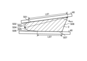
- FIG. 3 is an explanatory diagram showing a method for evaluating crystallites.
- the crystallite 2 has a polygonal cross section.
- the crystallite 2 shown by way of example in FIG. 3 has an octagonal contour with sides S01 to S08.
- a scale (or ruler) 40 for example, is prepared and positioned along side S01 for an image of via conductor 20 including such a cross section. If the length of the portion of the side S01 along the scale (or ruler) 40 is 1/2 or more of the longest diameter d MAX of the crystallite 2, it is defined as a "straight side". .
- the other sides S02 to S08 are evaluated as to whether or not they are “linear sides” in the same manner as the side S01.
- the side S01 having the length L01 and the side S07 having the length L07 are evaluated as "linear sides”. That is, the crystallite 2 shown in FIG. 3 has two “linear sides”.
- the longest diameter d MAX of the crystallite 2 is preferably 1 ⁇ m or more and 10 ⁇ m or less.
- the evaluation described above is repeated for each side of each of the plurality of crystallites 2 .
- the plurality of crystallites 2 may have 50% or more of the crystallites 2 having two or more linear sides.
- the decrease in the interfacial conductivity at frequencies of 1 GHz to 49 GHz can be reduced, for example. .
- the interfacial conductivity at high frequencies can be increased.
- a sample for cross-sectional observation is prepared by cutting the wiring board 1 where the cross section of the via conductor 20 can be seen and polishing the cut surface.
- the polished surface is analyzed using the EBSD method.
- the photographing range of the sample in the thickness direction and the length direction of via conductor 20 is set as follows.
- the number of crystallites 2 included in the imaging range is, for example, 50 or more and 100 or less.
- a range of about 20 ⁇ m in the thickness direction and width direction of the via conductor 20 is photographed. Moreover, it may be in the range of 10 ⁇ m or more and 20 ⁇ m or less.
- the conductor layer 30 has conductivity and is arranged in a predetermined pattern on the surface of the insulating layer 10 and between the insulating layers 10 adjacent to each other. That is, in the wiring board 1 , the conductor layer 30 is positioned along the surface of the insulating layer 10 . The conductor layers 30 are positioned at predetermined intervals with the insulating layer 10 interposed therebetween. When the two conductor layers 30 are arranged at positions sandwiching one insulating layer 10, the overlapping portion of the two conductor layers 30 arranged with one insulating layer 10 interposed therebetween functions as a capacitor. In other words, in the wiring board 1 , the portion that functions as a capacitor is the overlapping portion of the two conductor layers 30 sandwiching one insulating layer 10 .
- the conductor layer 30 contains copper as a main component. Specifically, the conductor layer 30 contains 50% by mass or more of copper. The conductor layer 30 may contain 70% by mass or more of copper.
- the conductor layer 30 is a sintered body of a plurality of metal particles whose main component is copper.
- FIG. 4 is an enlarged view of area B shown in FIG.
- the conductor layer 30 may also include crystallites 3 that are polygonal in cross section, as shown in FIG.
- the plurality of adjacent crystallites 3 in the conductor layer 30 there may be included those in contact with the linear sides of the respective crystallites 3 as grain boundaries.
- the plurality of crystallites 3 may have 50% or more of the crystallites 3 having two or more linear sides.
- the average particle size of the metal particles in the via conductors 20 may be larger than the average particle size of the metal particles in the conductor layer 30 .
- the average particle size of the metal particles of the via conductors 20 and the average particle size of the metal particles of the conductor layer 30 are 6.6:1 to 1.4:1, particularly 5:1 to 5:1.
- the wiring substrate 1 with high performance can be obtained.
- the average grain size of the crystallites 2 contained in the conductor layer 30 is 1, the average grain size of the crystallites 2 contained in the via conductor 20 is, for example, 1.4 times or more and 6.6 times or less. is preferably in the range of 1.3 times or more and 5 times or less.
- the obtained wiring board 1 is cut or polished to prepare a sample in which the cross section of the via conductor 20 is exposed.
- the cross section of wiring board 1 including the cross section of via conductors 20 is preferably finished to a mirror level.
- the cross section of via conductor 20 is observed using the EBSD method, and a photograph of the cross section is taken. The following measurements are made using photographs taken.
- one region is specified in which, for example, 20 or more and 30 or less crystallites 2 are included.
- the shape of the specified range is preferably circular or rectangular.
- the specified location may also include, for example, spherical crystallites 2 .
- the average grain size of the crystallites 2 in the conductor layer 30 and in the connecting portion between the via conductor 20 and the conductor layer 30 is obtained by the same method.
- the via conductors 20 and the conductor layer 30 viewed in cross section may contain 70% or more of the metal component per unit area.
- the metal components of via conductors 20 and conductor layer 30 are densified, and wiring board 1 with high performance is obtained.
- the ratio of metal components contained in the via conductors 20 and the conductor layer 30 was also evaluated by observing and photographing the same locations as the cross-sectional photographs used to determine the average grain size of the crystallites 2 described above with an electron microscope. It is better to use things.
- the area A1 of the void is obtained by image analysis from a photograph of the cross section of the via conductor 20 and the conductor layer 30, and the ratio of (A0-A1)/A0 is obtained when the area of the specified range is defined as the total area A0.
- the via conductors 20 and the conductor layer 30 may contain silica.
- silica may have, for example, an average particle size of 10 nm or more and 30 nm or less.
- silica may be contained in a ratio of 0.3 parts by mass or more and 0.8 parts by mass or less with respect to 100 parts by mass of Cu.
- the content of silica should be less than the content of the glass components other than silica.
- via conductors 20 and conductor layer 30 may contain borosilicate glass.
- Such silica may have, for example, an average particle size of 50 nm or more and 200 nm or less.
- the borosilicate glass may be contained at a ratio of about 1 part by mass with respect to 100 parts by mass of Cu.
- the wiring board 1 may have a connecting portion 25.
- the connecting portion 25 is a portion where the end portion of the via conductor 20 and the conductor layer 30 are in contact with each other.
- FIG. 5 is an enlarged view of area C shown in FIG.
- connecting portion 25 may have crystallites 4 whose grain size is smaller than the average grain size of crystallites 2 and 3 of via conductor 20 and conductor layer 30 . This densifies the connecting portion 25 and enhances the adhesion between the via conductor 20 and the conductor layer 30 .
- the connecting portion 25 may have one or a plurality of such crystallites 4 .
- a mixture of 40 wt% alumina particles and 60 wt% borosilicate glass was prepared as a material for the insulating layer 10.
- Such a mixture is a glass-ceramic raw material with a firing temperature of 900° C. or higher and 1000° C. or lower.
- the organic binder 20 parts by mass of isobutyl methacrylate resin and dibutyl phthalate were used with respect to 100 parts by mass of the glass-ceramics raw material, and a green sheet having a thickness of 100 ⁇ m was produced by doctor blade molding.
- silica particles with an average particle size of 20 nm, and borosilicate glass particles with an average particle size of 100 nm were prepared.
- Silica particles had a ratio of an integrated amount of 70% or more with a lower limit of 10 nm and an upper limit of 30 nm.
- organic binder a mixed solvent of isobutyl methacrylate resin, butyl carbitol acetate, and dibutyl phthalate was used.
- Isobutyl methacrylate resin was added at a rate of 5 parts by mass with respect to 100 parts by mass of copper powder, and a mixed solvent of butyl carbitol acetate and dibutyl phthalate was added to obtain 100 parts by mass of copper powder and 0.3 parts by mass of copper powder.
- Conductive pastes containing silica particles and 1 part by mass of borosilicate glass particles were each prepared.
- sample no. 6, 12, 18, and 24, conductor pastes containing 100 parts by weight of copper powder and 1 part by weight of borosilicate glass particles were prepared, respectively.
- a substantially cylindrical conductor paste was printed so as to penetrate the produced green sheet, and the conductor paste was printed in a predetermined area on both surfaces of the green sheet to produce a laminate and fired. Firing was performed in a reducing atmosphere using a hydrogen-nitrogen mixed gas with a maximum temperature of 930° C. and a holding time of 2 hours.
- the laminated body was prepared by stacking two insulating layers 10 having a thickness of 35 ⁇ m and thirteen insulating layers 10 having a thickness of 25 ⁇ m, thereby stacking fifteen layers.
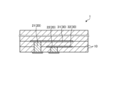
- FIG. 6 is a cross-sectional view showing an outline of the sample according to the example.
- a wiring board 1 as a sample according to the example was obtained by stacking two insulating layers 10 having a thickness of 35 ⁇ m and thirteen insulating layers 10 having a thickness of 25 ⁇ m, thereby stacking fifteen layers.
- the evaluation layer corresponding to the distance between the conductor layer 31 electrically connected to the via conductor 21 and the conductor layer 32 electrically connected to the via conductor 22 was set to 25 ⁇ m, and the via conductor 21 and the via conductor 22 were separated.
- a predetermined voltage was applied between , and the electrostatic capacity (capacitor capacity) between the conductor layers 31 and 32 was measured. Such measurements were performed at 30 locations, and the deviation (variation coefficient 3CV: 3 x standard deviation ( ⁇ )/average value (x)) was calculated. The results are shown in FIG.
- FIG. 7 is a diagram showing evaluation results of the wiring board according to the example.
- the average grain size of the crystallites was Except for No. 19, values corresponding to raw material particle sizes were shown.
- sample No. In the wiring boards according to Nos. 1 to 4, 7 to 10, 13 to 17, and 20 to 23, the 3CV was as small as 7 or less, and high performance wiring boards were obtained. In particular, sample no. In the wiring boards according to Nos. 1 to 3, 7 to 10, 14 to 17, and 21 to 23, 3CV was as small as 5 or less, and wiring boards with extremely high performance were obtained.
- One reason for this is considered to be that the grain size of the raw material in the via conductor 20 is equal to or smaller than the grain size of the raw material in the conductor layer 30 .
- the grain size of the raw material in the via conductor 20 was much larger than the grain size of the raw material in the conductor layer 30, and the average grain size of the crystallites in the via conductor 20 and the conductor layer 30 became approximately the same due to grain growth. This is considered to be one of the reasons.
- the via conductors and conductor layers to which silica particles were added contained polygonal crystallites in the range of 50% or more and 80% or less. Further, in each of these samples, crystallites having a grain size smaller than the average grain size of crystallites possessed by the via conductor and the conductor layer were observed in the connection portion where the end portion of the via conductor and the conductor layer were in contact.
Landscapes
- Engineering & Computer Science (AREA)
- Microelectronics & Electronic Packaging (AREA)
- Chemical & Material Sciences (AREA)
- Ceramic Engineering (AREA)
- Inorganic Chemistry (AREA)
- Manufacturing & Machinery (AREA)
- Production Of Multi-Layered Print Wiring Board (AREA)
- Parts Printed On Printed Circuit Boards (AREA)
Priority Applications (4)
| Application Number | Priority Date | Filing Date | Title |
|---|---|---|---|
| JP2023570947A JP7739463B2 (ja) | 2021-12-28 | 2022-12-22 | 配線基板 |
| CN202280082530.8A CN118511657A (zh) | 2021-12-28 | 2022-12-22 | 布线基板 |
| US18/721,714 US20250120016A1 (en) | 2021-12-28 | 2022-12-22 | Wiring board |
| EP22915928.0A EP4460156A1 (en) | 2021-12-28 | 2022-12-22 | Wiring board |
Applications Claiming Priority (2)
| Application Number | Priority Date | Filing Date | Title |
|---|---|---|---|
| JP2021215303 | 2021-12-28 | ||
| JP2021-215303 | 2021-12-28 |
Publications (1)
| Publication Number | Publication Date |
|---|---|
| WO2023127705A1 true WO2023127705A1 (ja) | 2023-07-06 |
Family
ID=86999222
Family Applications (1)
| Application Number | Title | Priority Date | Filing Date |
|---|---|---|---|
| PCT/JP2022/047494 Ceased WO2023127705A1 (ja) | 2021-12-28 | 2022-12-22 | 配線基板 |
Country Status (5)
| Country | Link |
|---|---|
| US (1) | US20250120016A1 (https=) |
| EP (1) | EP4460156A1 (https=) |
| JP (1) | JP7739463B2 (https=) |
| CN (1) | CN118511657A (https=) |
| WO (1) | WO2023127705A1 (https=) |
Citations (4)
| Publication number | Priority date | Publication date | Assignee | Title |
|---|---|---|---|---|
| JP2003277852A (ja) | 2002-03-25 | 2003-10-02 | Kyocera Corp | 銅メタライズ組成物およびセラミック配線基板 |
| JP2004134378A (ja) * | 2002-07-17 | 2004-04-30 | Ngk Spark Plug Co Ltd | 銅ペーストとそれを用いた配線基板 |
| JP2005243789A (ja) * | 2004-02-25 | 2005-09-08 | Kyocera Corp | セラミック電子部品の製法 |
| JP2019207977A (ja) | 2018-05-30 | 2019-12-05 | 京セラ株式会社 | 配線基板 |
-
2022
- 2022-12-22 EP EP22915928.0A patent/EP4460156A1/en not_active Withdrawn
- 2022-12-22 JP JP2023570947A patent/JP7739463B2/ja active Active
- 2022-12-22 WO PCT/JP2022/047494 patent/WO2023127705A1/ja not_active Ceased
- 2022-12-22 US US18/721,714 patent/US20250120016A1/en active Pending
- 2022-12-22 CN CN202280082530.8A patent/CN118511657A/zh active Pending
Patent Citations (4)
| Publication number | Priority date | Publication date | Assignee | Title |
|---|---|---|---|---|
| JP2003277852A (ja) | 2002-03-25 | 2003-10-02 | Kyocera Corp | 銅メタライズ組成物およびセラミック配線基板 |
| JP2004134378A (ja) * | 2002-07-17 | 2004-04-30 | Ngk Spark Plug Co Ltd | 銅ペーストとそれを用いた配線基板 |
| JP2005243789A (ja) * | 2004-02-25 | 2005-09-08 | Kyocera Corp | セラミック電子部品の製法 |
| JP2019207977A (ja) | 2018-05-30 | 2019-12-05 | 京セラ株式会社 | 配線基板 |
Also Published As
| Publication number | Publication date |
|---|---|
| JPWO2023127705A1 (https=) | 2023-07-06 |
| JP7739463B2 (ja) | 2025-09-16 |
| US20250120016A1 (en) | 2025-04-10 |
| EP4460156A1 (en) | 2024-11-06 |
| CN118511657A (zh) | 2024-08-16 |
Similar Documents
| Publication | Publication Date | Title |
|---|---|---|
| KR102102800B1 (ko) | 외부전극용 도전성 페이스트 및 그 외부전극용 도전성 페이스트를 이용하여 제조하는 전자부품의 제조 방법 | |
| KR101699389B1 (ko) | 적층 세라믹 콘덴서 및 그 제조방법 | |
| US20090025855A1 (en) | Insulating Substrate and Manufacturing Method Therefor, and Multilayer Wiring Board and Manufacturing Method Therefor | |
| JP3350949B2 (ja) | 導電性ペースト | |
| JP5071559B2 (ja) | 積層型セラミック電子部品およびその製造方法 | |
| US6623845B1 (en) | Glass-ceramic composition, and electronic component and multilayer LC composite component using the same | |
| WO2023127705A1 (ja) | 配線基板 | |
| CN1323969C (zh) | 玻璃陶瓷组合物及使用了该组合物的电子部件和叠层式lc复合部件 | |
| WO2023189338A1 (ja) | 配線基板 | |
| US20250185162A1 (en) | Wiring board | |
| JPH06172017A (ja) | セラミツクス基板用グリーンシート及びセラミツクス基板 | |
| JPS63209150A (ja) | 低誘電率絶縁体基板 | |
| JPH09153681A (ja) | 低温焼成基板製造用内蔵抵抗ペースト | |
| EP4535931A1 (en) | Circuit component | |
| JP2004055557A (ja) | 銅ペーストとそれを用いた配線基板及び配線基板の製造方法 | |
| WO2022163574A1 (ja) | 配線基板 | |
| JPH07326537A (ja) | セラミック積層電子部品の製造方法 | |
| JPH01183448A (ja) | 回路基板 | |
| JP2002299820A (ja) | セラミック部品の製造方法 | |
| CN121311955A (zh) | 层叠陶瓷电容器 | |
| TW202207244A (zh) | 厚膜電阻糊、厚膜電阻體、及電子元件 | |
| JP2004319527A (ja) | セラミック配線基板およびその製造方法 | |
| JPH0752696B2 (ja) | 積層形セラミツクコンデンサ及びその製造方法 | |
| JP2008159940A (ja) | 多層配線基板およびその製造方法 | |
| JPH02251121A (ja) | 磁器コンデンサの電極用導電性ペースト |
Legal Events
| Date | Code | Title | Description |
|---|---|---|---|
| 121 | Ep: the epo has been informed by wipo that ep was designated in this application |
Ref document number: 22915928 Country of ref document: EP Kind code of ref document: A1 |
|
| WWE | Wipo information: entry into national phase |
Ref document number: 202280082530.8 Country of ref document: CN |
|
| WWE | Wipo information: entry into national phase |
Ref document number: 18721714 Country of ref document: US |
|
| WWE | Wipo information: entry into national phase |
Ref document number: 2023570947 Country of ref document: JP |
|
| NENP | Non-entry into the national phase |
Ref country code: DE |
|
| ENP | Entry into the national phase |
Ref document number: 2022915928 Country of ref document: EP Effective date: 20240729 |
|
| WWP | Wipo information: published in national office |
Ref document number: 18721714 Country of ref document: US |
|
| WWW | Wipo information: withdrawn in national office |
Ref document number: 2022915928 Country of ref document: EP |