EP4460156A1 - Wiring board - Google Patents
Wiring board Download PDFInfo
- Publication number
- EP4460156A1 EP4460156A1 EP22915928.0A EP22915928A EP4460156A1 EP 4460156 A1 EP4460156 A1 EP 4460156A1 EP 22915928 A EP22915928 A EP 22915928A EP 4460156 A1 EP4460156 A1 EP 4460156A1
- Authority
- EP
- European Patent Office
- Prior art keywords
- conductor
- via conductor
- layer
- wiring board
- conductor layer
- Prior art date
- Legal status (The legal status is an assumption and is not a legal conclusion. Google has not performed a legal analysis and makes no representation as to the accuracy of the status listed.)
- Withdrawn
Links
Images


Classifications
-
- H—ELECTRICITY
- H05—ELECTRIC TECHNIQUES NOT OTHERWISE PROVIDED FOR
- H05K—PRINTED CIRCUITS; CASINGS OR CONSTRUCTIONAL DETAILS OF ELECTRIC APPARATUS; MANUFACTURE OF ASSEMBLAGES OF ELECTRICAL COMPONENTS
- H05K1/00—Printed circuits
- H05K1/02—Details
- H05K1/11—Printed elements for providing electric connections to or between printed circuits
- H05K1/115—Via connections; Lands around holes or via connections
-
- H—ELECTRICITY
- H05—ELECTRIC TECHNIQUES NOT OTHERWISE PROVIDED FOR
- H05K—PRINTED CIRCUITS; CASINGS OR CONSTRUCTIONAL DETAILS OF ELECTRIC APPARATUS; MANUFACTURE OF ASSEMBLAGES OF ELECTRICAL COMPONENTS
- H05K1/00—Printed circuits
- H05K1/02—Details
- H05K1/03—Use of materials for the substrate
- H05K1/0306—Inorganic insulating substrates, e.g. ceramic, glass
-
- H—ELECTRICITY
- H05—ELECTRIC TECHNIQUES NOT OTHERWISE PROVIDED FOR
- H05K—PRINTED CIRCUITS; CASINGS OR CONSTRUCTIONAL DETAILS OF ELECTRIC APPARATUS; MANUFACTURE OF ASSEMBLAGES OF ELECTRICAL COMPONENTS
- H05K1/00—Printed circuits
- H05K1/02—Details
- H05K1/09—Use of materials for the conductive, e.g. metallic pattern
-
- H—ELECTRICITY
- H05—ELECTRIC TECHNIQUES NOT OTHERWISE PROVIDED FOR
- H05K—PRINTED CIRCUITS; CASINGS OR CONSTRUCTIONAL DETAILS OF ELECTRIC APPARATUS; MANUFACTURE OF ASSEMBLAGES OF ELECTRICAL COMPONENTS
- H05K3/00—Apparatus or processes for manufacturing printed circuits
- H05K3/40—Forming printed elements for providing electric connections to or between printed circuits
-
- H—ELECTRICITY
- H05—ELECTRIC TECHNIQUES NOT OTHERWISE PROVIDED FOR
- H05K—PRINTED CIRCUITS; CASINGS OR CONSTRUCTIONAL DETAILS OF ELECTRIC APPARATUS; MANUFACTURE OF ASSEMBLAGES OF ELECTRICAL COMPONENTS
- H05K2201/00—Indexing scheme relating to printed circuits covered by H05K1/00
- H05K2201/02—Fillers; Particles; Fibers; Reinforcement materials
- H05K2201/0203—Fillers and particles
- H05K2201/0263—Details about a collection of particles
- H05K2201/0266—Size distribution
-
- H—ELECTRICITY
- H05—ELECTRIC TECHNIQUES NOT OTHERWISE PROVIDED FOR
- H05K—PRINTED CIRCUITS; CASINGS OR CONSTRUCTIONAL DETAILS OF ELECTRIC APPARATUS; MANUFACTURE OF ASSEMBLAGES OF ELECTRICAL COMPONENTS
- H05K2201/00—Indexing scheme relating to printed circuits covered by H05K1/00
- H05K2201/03—Conductive materials
- H05K2201/0332—Structure of the conductor
- H05K2201/0335—Layered conductors or foils
- H05K2201/0338—Layered conductor, e.g. layered metal substrate, layered finish layer or layered thin film adhesion layer
Definitions
- An embodiment of the present disclosure relates to a wiring board.
- a wiring board including an insulation layer made of ceramic, a conductor layer containing copper as a main component, and a via conductor is known.
- Such a wiring board is obtained by, for example, simultaneously firing a conductor layer material and a via conductor material in which a metal oxide is added to copper powder, and a glass ceramic as an insulation layer material.
- a wiring board includes an insulation layer, a via conductor, and a conductor layer.
- the insulation layer is made of a glass ceramic.
- the via conductor is disposed penetrating the insulation layer.
- the conductor layer is located in a direction along a surface of the insulation layer.
- the via conductor and the conductor layer are connected to each other, and are each a sintered body of a plurality of metal particles containing copper as a main component.
- An average particle diameter of the metal particles included in the via conductor is larger than the average particle diameter of the metal particles included in the conductor layer.
- the via conductor and the conductor layer in a cross-sectional view each contain 70% or more of a metal component per unit area.
- an electrostatic capacitance of a capacitor formed between the conductor layers overlapping in the layering direction of the insulation layers may vary, and thus the wiring board has room for improvement.
- the capacitor formed between the conductor layers overlapping in the layering direction of the insulation layers may be hereinafter referred to as a built-in capacitor.
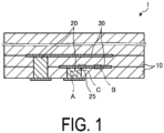
- FIG. 1 is a cross-sectional view illustrating an example of a wiring board according to an embodiment.
- a wiring board 1 according to the embodiment includes an insulation layer 10, a via conductor 20, and a conductor layer 30.
- the insulation layer 10 is made of a glass ceramic.
- the wiring board 1 can be manufactured by simultaneously firing a green sheet, which is the material of the insulation layer 10, and the conductive paste containing the metal particles, which is the material of the via conductor 20 and the conductor layer 30.
- the via conductor 20 has conductivity and is disposed penetrating the insulation layer 10.
- the via conductor 20 contains copper as a main component. Specifically, the via conductor 20 contains 50 mass% or more of copper. The via conductor 20 may contain 70 mass% or more of copper.
- the via conductor 20 is a sintered body of a plurality of metal particles containing copper as a main component.
- the via conductor 20 includes a crystallite 2 having a polygonal shape in a cross-sectional view.
- the state in which the via conductor 20 includes the polygonal crystallite 2 can be confirmed by analysis using an electron back scattered diffraction (EBSD) pattern method.
- EBSD electron back scattered diffraction
- FIG. 2 is an enlarged view of a region A illustrated in FIG. 1 .
- the via conductor 20 has a structure of two groups of crystallites as schematically illustrated in FIG. 2 .
- a plurality of adjacent crystallites 2 may be in contact with each other with a linear side of each crystallite 2 as a grain boundary.
- the via conductor 20 has a crystal structure in which the crystallites 2 are in contact with each other at their linear sides.
- the contact area between the crystallites 2 is large as compared with the case where the crystallite 2 has a spherical shape or a particle shape close to a spherical shape.
- the interface conductivity at a high frequency can be increased, so that a wiring board having a high interface conductivity at a high frequency can be obtained.
- FIG. 3 is an explanatory diagram illustrating an evaluation method for crystallites.
- the crystallite 2 has a polygonal cross section.
- the crystallite 2 illustrated in FIG. 3 has an octagonal contour having sides S01 to S08.
- a scale (or ruler) 40 is prepared and located along the side S01 in the captured image of the via conductor 20 including such a cross section.
- the side S01 is defined as a "linear side” when a portion of the side S01 extending along the scale (or ruler) 40 is equal to or longer than a half of the longest diameter d MAX of the crystallite 2.
- the side S01 having a length L01 and the side S07 having a length L07 are evaluated as "linear sides". That is, the crystallite 2 illustrated in FIG. 3 has two "linear sides".
- the longest diameter d MAX of the crystallite 2 may be 1 ⁇ m or more and 10 ⁇ m or less.
- the above-described evaluation is repeated for each side of each of the plurality of crystallites 2.
- the plurality of crystallites 2 may include 50% or more of crystallites 2 having two or more linear sides.
- a decrease in the interface conductivity at frequencies of 1 GHz to 49 GHz can be reduced. Accordingly, interface conductivity at high frequencies can be enhanced.
- the wiring board 1 is cut at a position where the cross section of the via conductor 20 can be seen, and the cut surface is polished to prepare a sample for observing the cross section.
- the polished surface is analyzed using the EBSD method.
- the imaging range of the sample in the thickness direction and the length direction of the via conductor 20 is set as follows, for example.
- the number of crystallites 2 included in the imaging range is, for example, 50 or more and 100 or less.
- a range of about 20 ⁇ m in the thickness direction and the width direction of the via conductor 20 is imaged.
- a range of 10 ⁇ m or more to 20 ⁇ m or less in the thickness direction and the width direction of the via conductor 20 may be imaged.
- the conductor layer 30 has conductivity and is disposed in a predetermined pattern shape on the surface of the insulation layer 10 and between the insulation layers 10 adjacent to each other. That is, in the wiring board 1, the conductor layer 30 is located in a direction along the surface of the insulation layer 10. The conductor layers 30 are located at predetermined intervals with the insulation layer 10 interposed therebetween. When two conductor layers 30 are arranged at such a position that one insulation layer 10 is sandwiched between the conductor layers 30, a portion where the two conductor layers 30 overlap each other via the one insulation layer 10 in the arrangement is a portion that functions as a capacitor. In other words, in the wiring board 1, a portion that functions as a capacitor is a portion where two conductor layers 30 with which one insulation layer 10 is sandwiched overlap each other.
- the conductor layer 30 contains copper as a main component. Specifically, the conductor layer 30 contains 50 mass% or more of copper. The conductor layer 30 may contain 70 mass% or more of copper.
- the conductor layer 30 is a sintered body of a plurality of metal particles containing copper as a main component.
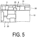
- FIG. 4 is an enlarged view of a region B illustrated in FIG. 1 .
- the conductor layer 30 may also include a crystallite 3 having a polygonal shape in a cross-sectional view.
- a plurality of adjacent crystallites 3 may be in contact with each other with the linear side of each crystallite 3 as a grain boundary.
- the plurality of crystallites 3 may include 50% or more of crystallites 3 having two or more linear sides.
- the average particle diameter of the metal particles included in the via conductor 20 may be larger than the average particle diameter of the metal particles included in the conductor layer 30. Specifically, for example, by setting the average particle diameter of the metal particles included in the via conductor 20 and the average particle diameter of the metal particles included in the conductor layer 30 to 6.6:1 to 1.4:1, particularly 5:1 to 1.3:1, the wiring board 1 having high performance is obtained.
- the average particle diameter of the crystallites 2 included in the conductor layer 30 is set to 1
- the average particle diameter of the crystallites 2 included in the via conductor 20 is, for example, in a range of 1.4 times or more and 6.6 times or less, and particularly, may be in a range of 1.3 times or more and 5 times or less.
- the obtained wiring board 1 is cut or polished to produce a sample in which the cross section of the via conductor 20 is exposed.
- the cross section of the wiring board 1 including the cross section of the via conductor 20 is preferably finished to a mirror surface level.
- the cross section of the via conductor 20 is observed by using the EBSD method, and the image of the cross section is captured. The following measurements are performed using the image captured.
- one region where 20 or more and 30 or less crystallites 2 are included is specified.
- the shape of the specified range is preferably circular or quadrangular.
- Image analysis is then performed on each crystallite 2 present in the specified place, and the area of the crystallite 2 is obtained. Next, an area obtained by converting the obtained area into a circle is obtained. The diameter is then determined from the area converted into a circle. The diameter thus obtained is defined as the particle diameter of each crystallite 2. Such measurement is performed on the crystallites 2 present in the specified place, and the average particle diameter is obtained. In addition to the polygonal crystallites 2, other crystallites 2, for example, spherical crystallites 2 may be included in the specified place. The average particle diameters of the crystallites 2 in the conductor layer 30 and the connection portion between the via conductor 20 and the conductor layer 30 are also obtained by the same method or a similar method. When a voltage is applied to the wiring board 1, the via conductor 20 and the conductor layer 30 are electrically connected to each other.
- the via conductor 20 and the conductor layer 30 in a cross-sectional view may contain 70% or more of a metal component per unit area.
- the metal components of the via conductor 20 and the conductor layer 30 are densified, and the wiring board 1 having high performance is obtained.
- the ratio of the metal component contained in each of the via conductor 20 and the conductor layer 30 may also be evaluated by observing and imaging a place the same as or similar to the place of the cross-sectional image used for obtaining the average particle diameter of the crystallite 2, with an electron microscope.
- An area A1 of voids is obtained by image analysis from images obtained by imaging cross sections of the via conductor 20 and the conductor layer 30, and a ratio of (A0 - A1)/A0 is obtained when an area of a specified range is defined as a total area A0.
- the via conductor 20 and the conductor layer 30 may contain silica.
- the silica may have, for example, an average particle diameter of 10 nm or more and 30 nm or less.
- the silica may be contained at a ratio of 0.3 parts by mass or more and 0.8 parts by mass or less with respect to 100 parts by mass of Cu.
- the content of silica is preferably less than the content of the glass component other than silica.
- the via conductor 20 and the conductor layer 30 may contain borosilicate glass.
- the silica may have, for example, an average particle diameter of 50 nm or more and 200 nm or less.
- the borosilicate glass may be contained at a ratio of about 1 part by mass with respect to 100 parts by mass of Cu.
- the wiring board 1 may include a connection portion 25.
- the connection portion 25 refers to a portion where the end portion of the via conductor 20 and the conductor layer 30 are in contact with each other.
- FIG. 5 is an enlarged view of a region C illustrated in FIG. 1 .
- the connection portion 25 may include a crystallite 4 having a particle diameter smaller than the average particle diameters of the crystallites 2 and 3 included in the via conductor 20 and the conductor layer 30, respectively.
- the connection portion 25 is densified, and the adhesion between the via conductor 20 and the conductor layer 30 is increased.
- the connection portion 25 may include one or more such crystallites 4.
- Samples No. 1 to No. 24 simulating the wiring board 1 according to the embodiment were produced, and the deviations of the capacitor capacitances were evaluated.
- a mixture of 40 wt.% alumina particles and 60 wt.% borosilicate glass was prepared as the material of the insulation layer 10.
- the mixture is a glass ceramic raw material having a firing temperature of 900°C or higher and 1000°C or lower.
- As an organic binder 20 parts by mass of isobutyl methacrylate resin and dibutyl phthalate were used with respect to 100 parts by mass of the glass ceramic raw material, and a green sheet having a thickness of 100 ⁇ m was produced by doctor blade molding.
- silica particles having an average particle diameter of 20 nm, and borosilicate glass particles having an average particle diameter of 100 nm were prepared.
- the silica particles have a percentage of the integrated amount of the lower limit of 10 nm and the upper limit of 30 nm of 70% or more.
- the organic binder isobutyl methacrylate resin and a mixed solvent of butyl carbitol acetate and dibutyl phthalate were used.
- a conductive paste containing 100 parts by mass of copper powder, 0.3 parts by mass of silica particles, and 1 part by mass of borosilicate glass particles was prepared by adding 5 parts by mass of isobutyl methacrylate resin to 100 parts by mass of copper powder and further adding a mixed solvent of butyl carbitol acetate and dibutyl phthalate.
- conductive pastes containing 100 parts by mass of copper powder and 1 part by mass of borosilicate glass particles were prepared.
- a conductive paste having a substantially columnar shape was printed so as to penetrate the prepared green sheet, and the conductive paste was printed on both surfaces of the green sheet in a predetermined area to prepare a laminate, and the laminate was fired. Firing was performed in a reducing atmosphere using a nitrogen-hydrogen mixed gas at a maximum temperature of 930°C for a holding time of 2 hours.
- the laminate a laminate in which two insulation layers 10 each having a thickness of 35 ⁇ m and 13 insulation layers 10 each having a thickness of 25 ⁇ m were layered to form 15 layers was used.
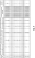
- FIG. 6 is a cross-sectional view schematically illustrating a sample according to an example.
- the wiring board 1 as a sample according to the example, a wiring board in which two insulation layers 10 each having a thickness of 35 ⁇ m and 13 insulation layers 10 each having a thickness of 25 ⁇ m were layered to form 15 layers was used.
- the evaluation layer corresponding to the interval between the conductor layer 31 electrically connected to the via conductor 21 and the conductor layer 32 electrically connected to the via conductor 22 was set to 25 ⁇ m, a predetermined voltage was applied between the via conductor 21 and the via conductor 22, and the electrostatic capacitance (capacitor capacitance) between the conductor layers 31, 32 was measured. This measurement was performed at 30 points, and the deviation (variation coefficient 3CV: 3 ⁇ standard deviation ( ⁇ )/average value (x)) was calculated. The results are shown in FIG. 7 .
- FIG. 7 is a diagram illustrating evaluation results of the wiring boards according to the example.
- FIG. 7 shows the average particle diameters (raw material particle diameters) of the copper powders as raw materials of the via conductors 20 and the conductor layers 30, the ratios (particle diameter ratios) of the average particle diameters of the copper powders as raw materials of the via conductors 20 and the conductor layers 30, the presence or absence of the silica particles in the conductive paste, the contents of the metal components per unit area in the via conductors 20 and the conductor layers 30 in cross-sectional view (area ratios of the metal components), the comparison of the average particle diameters of the crystallites in the via conductors 20 and the conductor layers 30, and the deviations (3CV) of the capacitor capacitances.
- the average particle diameters of the crystallites were each a value corresponding to the raw material particle diameter except for Sample No. 19.
- the 3CV was as small as 7 or less, and high-performance wiring boards were obtained.
- the 3CV was as small as 5 or less, and the wiring boards having extremely high performance were obtained.
- the 3CV was more than 7, and the wiring boards having low performance were obtained. Presumably, this is partly because the raw material particle diameter in the via conductor 20 is equal to or less than the raw material particle diameter in the conductor layer 30.
- the wiring board of Sample No. 19 also had a 3CV of more than 7, and the wiring board having low performance was obtained.
- the raw material particle diameter in the via conductor 20 was excessively larger than the raw material particle diameter in the conductor layer 30 and that the average particle diameters of the crystallites in the via conductor 20 and the conductor layer 30 became substantially equal to each other due to the grain growth.
- the copper particles having a smaller particle diameter grew to a size corresponding to the particle diameter of the copper particles having a larger particle diameter.
- a portion in which the coverage of the conductor layer 30 was low was observed, and the electrostatic capacitance was about 30% of the other samples.
- the wiring boards of Samples No. 6, No. 12, No. 18, and No. 24 each had a capacitor capacitance deviation (3CV) of more than 7, and the wiring boards having low performances were obtained.
- 3CV capacitor capacitance deviation
- each of the via conductor and the conductor layer to which the silica particles were added contained polygonal crystallites at a ratio in a range of 50% to 80%.
- crystallites having a particle diameter smaller than the average particle diameter of the crystallites included in the via conductor and the conductor layer were observed in the connection portion where the end portion of the via conductor and the conductor layer were in contact with each other.
Landscapes
- Engineering & Computer Science (AREA)
- Microelectronics & Electronic Packaging (AREA)
- Chemical & Material Sciences (AREA)
- Ceramic Engineering (AREA)
- Inorganic Chemistry (AREA)
- Manufacturing & Machinery (AREA)
- Production Of Multi-Layered Print Wiring Board (AREA)
- Parts Printed On Printed Circuit Boards (AREA)
Applications Claiming Priority (2)
| Application Number | Priority Date | Filing Date | Title |
|---|---|---|---|
| JP2021215303 | 2021-12-28 | ||
| PCT/JP2022/047494 WO2023127705A1 (ja) | 2021-12-28 | 2022-12-22 | 配線基板 |
Publications (1)
| Publication Number | Publication Date |
|---|---|
| EP4460156A1 true EP4460156A1 (en) | 2024-11-06 |
Family
ID=86999222
Family Applications (1)
| Application Number | Title | Priority Date | Filing Date |
|---|---|---|---|
| EP22915928.0A Withdrawn EP4460156A1 (en) | 2021-12-28 | 2022-12-22 | Wiring board |
Country Status (5)
| Country | Link |
|---|---|
| US (1) | US20250120016A1 (https=) |
| EP (1) | EP4460156A1 (https=) |
| JP (1) | JP7739463B2 (https=) |
| CN (1) | CN118511657A (https=) |
| WO (1) | WO2023127705A1 (https=) |
Family Cites Families (4)
| Publication number | Priority date | Publication date | Assignee | Title |
|---|---|---|---|---|
| JP2003277852A (ja) | 2002-03-25 | 2003-10-02 | Kyocera Corp | 銅メタライズ組成物およびセラミック配線基板 |
| JP4528502B2 (ja) * | 2002-07-17 | 2010-08-18 | 日本特殊陶業株式会社 | 配線基板 |
| JP2005243789A (ja) * | 2004-02-25 | 2005-09-08 | Kyocera Corp | セラミック電子部品の製法 |
| JP7207867B2 (ja) | 2018-05-30 | 2023-01-18 | 京セラ株式会社 | 配線基板 |
-
2022
- 2022-12-22 EP EP22915928.0A patent/EP4460156A1/en not_active Withdrawn
- 2022-12-22 JP JP2023570947A patent/JP7739463B2/ja active Active
- 2022-12-22 WO PCT/JP2022/047494 patent/WO2023127705A1/ja not_active Ceased
- 2022-12-22 US US18/721,714 patent/US20250120016A1/en active Pending
- 2022-12-22 CN CN202280082530.8A patent/CN118511657A/zh active Pending
Also Published As
| Publication number | Publication date |
|---|---|
| WO2023127705A1 (ja) | 2023-07-06 |
| JPWO2023127705A1 (https=) | 2023-07-06 |
| JP7739463B2 (ja) | 2025-09-16 |
| US20250120016A1 (en) | 2025-04-10 |
| CN118511657A (zh) | 2024-08-16 |
Similar Documents
| Publication | Publication Date | Title |
|---|---|---|
| KR102102800B1 (ko) | 외부전극용 도전성 페이스트 및 그 외부전극용 도전성 페이스트를 이용하여 제조하는 전자부품의 제조 방법 | |
| KR101699389B1 (ko) | 적층 세라믹 콘덴서 및 그 제조방법 | |
| KR101761753B1 (ko) | 세라믹 전자부품 | |
| KR101771019B1 (ko) | 적층 세라믹 콘덴서 및 적층 세라믹 콘덴서의 제조 방법 | |
| KR102015809B1 (ko) | 전자부품 및 그 제조 방법 | |
| CN105531774B (zh) | 层叠陶瓷电子部件 | |
| KR101912266B1 (ko) | 적층 세라믹 전자부품 및 이의 제조방법 | |
| KR20140123979A (ko) | 도전성 페이스트, 및 전자부품, 그리고 전자부품의 제조방법 | |
| US20090025855A1 (en) | Insulating Substrate and Manufacturing Method Therefor, and Multilayer Wiring Board and Manufacturing Method Therefor | |
| CN103515094A (zh) | 多层陶瓷电子元件 | |
| Higuchi et al. | LTCC system with new high-ɛr and high-Q material co-fired with conventional low-ɛr base material for wireless communications | |
| EP4460156A1 (en) | Wiring board | |
| CN118020391A (zh) | 配线基板 | |
| EP4503869A1 (en) | Wiring board | |
| KR20020035443A (ko) | 세라믹 커패시터 및 그의 제조방법 | |
| JP2020096120A (ja) | セラミックス配線基板及びその製造方法 | |
| EP4503867A1 (en) | Wiring board | |
| EP4535931A1 (en) | Circuit component | |
| US20240224422A1 (en) | Wiring board | |
| US20240304379A1 (en) | Multilayer coil component | |
| US20240304367A1 (en) | Multilayer coil component | |
| JP2892204B2 (ja) | 誘電体回路基板 | |
| Higuchi et al. | LTCCsystem with new high-and high-Q material co-fired with conventional low-base material for wireless communications | |
| JP2023010508A (ja) | キャパシタ部品及びキャパシタ部品の製造方法 | |
| JP2008159940A (ja) | 多層配線基板およびその製造方法 |
Legal Events
| Date | Code | Title | Description |
|---|---|---|---|
| STAA | Information on the status of an ep patent application or granted ep patent |
Free format text: STATUS: THE INTERNATIONAL PUBLICATION HAS BEEN MADE |
|
| PUAI | Public reference made under article 153(3) epc to a published international application that has entered the european phase |
Free format text: ORIGINAL CODE: 0009012 |
|
| STAA | Information on the status of an ep patent application or granted ep patent |
Free format text: STATUS: REQUEST FOR EXAMINATION WAS MADE |
|
| 17P | Request for examination filed |
Effective date: 20240612 |
|
| AK | Designated contracting states |
Kind code of ref document: A1 Designated state(s): AL AT BE BG CH CY CZ DE DK EE ES FI FR GB GR HR HU IE IS IT LI LT LU LV MC ME MK MT NL NO PL PT RO RS SE SI SK SM TR |
|
| DAV | Request for validation of the european patent (deleted) | ||
| DAX | Request for extension of the european patent (deleted) | ||
| STAA | Information on the status of an ep patent application or granted ep patent |
Free format text: STATUS: THE APPLICATION HAS BEEN WITHDRAWN |
|
| 18W | Application withdrawn |
Effective date: 20250926 |